EP1844472B1 - Magnetisches speichersystem unter verwendung von mram-abtaster - Google Patents
Magnetisches speichersystem unter verwendung von mram-abtaster Download PDFInfo
- Publication number
- EP1844472B1 EP1844472B1 EP06710706A EP06710706A EP1844472B1 EP 1844472 B1 EP1844472 B1 EP 1844472B1 EP 06710706 A EP06710706 A EP 06710706A EP 06710706 A EP06710706 A EP 06710706A EP 1844472 B1 EP1844472 B1 EP 1844472B1
- Authority
- EP
- European Patent Office
- Prior art keywords
- bit
- magnetization direction
- free
- magnetic field
- resistance value
- Prior art date
- Legal status (The legal status is an assumption and is not a legal conclusion. Google has not performed a legal analysis and makes no representation as to the accuracy of the status listed.)
- Expired - Lifetime
Links
Images


Classifications
-
- G—PHYSICS
- G11—INFORMATION STORAGE
- G11C—STATIC STORES
- G11C17/00—Read-only memories programmable only once; Semi-permanent stores, e.g. manually-replaceable information cards
- G11C17/02—Read-only memories programmable only once; Semi-permanent stores, e.g. manually-replaceable information cards using magnetic or inductive elements
-
- G—PHYSICS
- G11—INFORMATION STORAGE
- G11C—STATIC STORES
- G11C11/00—Digital stores characterised by the use of particular electric or magnetic storage elements; Storage elements therefor
- G11C11/02—Digital stores characterised by the use of particular electric or magnetic storage elements; Storage elements therefor using magnetic elements
- G11C11/16—Digital stores characterised by the use of particular electric or magnetic storage elements; Storage elements therefor using magnetic elements using elements in which the storage effect is based on magnetic spin effect
- G11C11/165—Auxiliary circuits
- G11C11/1673—Reading or sensing circuits or methods
Definitions
- the invention relates to a magnetic memory system as defined by claim 1.
- the invention further relates to an information carrier and a read circuit.
- the magnetoresistive elements typically comprise a stack of layers in which the resistance in the stack depends on the magnetization direction of the magnetic layers.
- the stack of layers comprises a free magnetic layer, which comprises two stable magnetization directions enabling the magnetoresistive element to store a logical value.
- EP0982736 discloses a magnetic memory cell including a data storage layer having an easy axis and a reference layer having an orientation of magnetization which is pinned in a direction that is off-axis with respect to the easy axis. This structure increases the signal obtainable during read operation on the magnetic memory cell notwithstanding the effects of magnetizations in the edge domains of the data storage layer. In addition, this structure allows high MRAM densities to be achieved using square-shaped memory cell structures.
- US6654278 discloses a magnetoresistive tunneling junction memory cell comprises a magnetoresistive tunneling barrier, a bit magnetic region, a reference magnetic region, and current lines for inducing an applied magnetic field in the bit and reference magnetic regions.
- the bit magnetic region has a bit magnetic moment that has a polarity in a bit easy axis when there is no applied magnetic field.
- the tunneling barrier and the bit and reference magnetic regions form a magnetoresistive tunneling junction device.
- An applied magnetic field changes the magnetic state of the reference magnetic region such that the magnetic state of the bit magnetic region can be determined by a magnetoresistive measurement.
- Read only magnetic information systems are, for example, disclosed in wo 2004/032149.
- a storage device comprising an information carrier part and a read-out part.
- the information carrier part comprises an information plane for cooperating with a read-out part.
- the read-out part comprises a two-dimensional array of electro-magnetic sensor elements. The read-out is done via a resistance measurement which relies on a magnetoresistance phenomenon.
- the electro-magnetic material which represents a bit at a bit location is constituted by hard magnetic material.
- the pattern of hard magnetic material is permanently magnetized in an external magnetic field, creating a pattern of magnetized magnetic bits all substantially having the same predetermined magnetic field direction and a magnetic field strength.
- the sensor comprises two ferromagnetic layers having different switching field strengths.
- the read-out of the sensor is done by measuring the resistance of the sensor while the sensor subsequently generates two magnetic field pulses which have a field strength in between the switching field strengths of the two ferromagnetic layers and which comprise opposite magnetic field directions.
- the layer with the higher switching field usually indicated as the fixed magnetic layer, will remain unchanged, while the magnetization of the layer with the lower switching field, usually indicated as the free magnetic layer, will be set by a first magnetic field pulse in a defined direction and then be reversed by a second magnetic field pulse.
- the magnetization direction of the free magnetic layer of the specific sensor cannot be reversed during the second magnetic field pulse and thus comprises an inverted magnetization direction compared to a sensor not having a magnetic bit present
- the two opposite magnetization directions of the free magnetic layer result in two sensed resistance values: a first resistance value at a first magnetization and a second resistance value (different from the first resistance value) at the reversed magnetization direction.
- the free magnetic layer in the sensor typically comprises two stable magnetization directions, resulting in the two resistance values in the sensor.
- the free magnetic layer may comprise any of the two stable magnetization directions.
- the magnetization direction of the free layer must be set by generating a magnetic field before reading the logical value of a bit location.
- a first bit magnetic field at one of the bit locations represents a first logical value selected from the group of three logical values by providing a first resistance value in a magnetoresistive element due to the free magnetization direction being substantially parallel to the magnetization is
- a second bit magnetic field at one of the bit locations represents a second logical value selected from the group of three logical values by providing a second resistance value in a magnetoresistive element due to the free magnetization direction rotation which results in an angle between the magnetization axis of the free magnetic layer and the free magnetic direction.
- the effect of the measures according to the invention is that the second bit magnetic field rotates the free magnetization direction which results in an angle between the free magnetization direction and the magnetization axis.
- the rotated free magnetization direction combined with the fixed magnetization direction of the fixed magnetic layer provides the second resistance value in the magnetoresistive element, which represents the second logical value.
- the free magnetization direction is substantially parallel to the magnetization axis of the free magnetic layer.
- the free magnetization direction parallel to the magnetization axis combined with the fixed magnetization direction of the fixed magnetic layer provides the first resistance value in the magnetoresistive element, which represents the first logical value.
- the free magnetic layer comprises two stable magnetization directions parallel to the magnetization axis
- the first logical value results from any of the two stable magnetization directions.
- the rotation of the free magnetization direction by the second bit magnetic field enables a distinction between the bit locations with the first bit magnetic field and bit locations with the second bit magnetic field.
- the magnetization direction which provides the second resistance value is not one of the two stable magnetization directions of the free magnetic layer and thus is different from the first resistance value, omitting the need for setting the magnetization direction of the free magnetic layer before read-out.
- the first bit magnetic field has a first magnetic field strength that is substantially zero.
- the free magnetic layer of the magnetoresistive element will be in any of the two stable magnetization directions and thus will be undefined.
- the bit locations which provide the second bit magnetic field to the sensor rotate the free magnetization direction which results in a resistance value in the magnetoresistive element which can be discriminated from any of the two stable magnetization directions of the free magnetization direction.
- the information layer substantially comprises a pattern of magnetic bits in which the presence or absence of the second bit magnetic field determines the logical value of the bit location. Because the bit magnetic fields present at the information layer all substantially have the same magnetization direction the manufacturing of the information layer is relatively easy.
- the second bit magnetic field has a second magnetization direction that is substantially perpendicular to the magnetization axis.
- the free magnetization direction is rotated by the second bit magnetic field to be substantially parallel to the second bit magnetic field and thus substantially perpendicular to the magnetization axis.
- the fixed magnetization direction is perpendicular to the magnetization axis.
- a benefit of this embodiment is that the two stable magnetization directions of the free magnetic layer both are perpendicular to the fixed magnetization direction and thus both substantially provide the same resistance value in the magnetoresistive element. Because the two stable magnetization directions of the free magnetic layer are represented by a single resistance value, the presence of the first or the second bit magnetic field at one of the bit locations can be identified by, for example, using a single reference value.
- a further bit magnetic field at one of the bit location represents a further logical value by providing a further resistance value in the magnetoresistive element due to the free magnetization direction having a further angle with the magnetization axis, the further angle being different from the angle causing the second logical value.
- the further bit magnetic field provides the further logical value which is different from the first logical value and the second logical value.
- a benefit of this embodiment is that the information stored in the pattern of magnetic bits represents a tertiary system in contrast with a binary system.
- the tertiary system as shown in this embodiment comprises three logical values: the first logical value, the second logical value and the further logical value.
- the system comprises an information carrier comprising an information layer which comprises a pattern of magnetic bits constituting an array of bit locations, a bit magnetic field at a bit location representing a logical value, the bit magnetic field having a bit magnetic field strength and a bit magnetization direction, wherein a first bit magnetic field at one of the bit locations represents a first logical value by providing a first resistance value in the magnetoresistive element due to the free magnetization direction being substantially parallel to the magnetization axis, a second bit magnetic field at one of the bit locations represents a second logical value by providing a second resistance value in the magnetoresistive element due to the free magnetization direction having an angle with the magnetization axis, and a further bit magnetic field at one of the bit locations represents a further logical value by providing a further resistance value in the magnetoresistive element due to the free magnetization direction having a further angle with the magnetization axis, the further angle being different from the angle causing the second logical value.
- the information carrier in this embodiment has a pattern of
- the system comprises a read circuit for reading a logical value from a sensor comprising a magnetoresistive element, wherein the read circuit comprises a reference circuit for providing at least two reference levels based on reference magnetoresistive elements and wherein the logical value is read by comparing a resistance value in the magnetoresistive element with the at least two reference levels.
- a benefit of this embodiment is that it enables a distinction in a system in which the free magnetization direction is undefined and may have any of the two stable magnetization directions. By comparing the resistance value with at least two reference levels, the resistance value caused by the second bit magnetic field can be distinguished from the two possible resistance values of the free magnetization direction parallel to the magnetization axis.
- a further benefit of this embodiment is that it enables the reading of, for example, a tertiary system in which three resistance values must be distinguished.
- the fixed magnetization direction is substantially parallel to the magnetization axis of the free magnetic layer.
- the sensed resistance value is typically a minimum resistance value, for example, representing the logical value "0".
- the sensed resistance value is typically a maximum resistance value, for example, representing the logical value "1 ".
- the bit magnetic field rotates the free magnetization direction away from the magnetization axis of the free magnetic layer which results in a sensed resistance value which is an intermediate resistance value between the maximum resistance value and the minimum resistance value, for example, representing a logical value "1/2".
- the fixed magnetization direction is substantially perpendicular to the magnetization axis of the free magnetic layer.
- Any of the two possible stable magnetization directions of the free magnetic layer provide substantially the same resistance value in the magnetoresistive element, being a resistance value substantially halfway between the maximum resistance value and the minimum resistance value.
- the second bit magnetic field for example, rotates the free magnetization direction parallel to the fixed magnetization direction, for example representing the logical value "0" or, for example rotates the free magnetization layer opposite to the fixed magnetization direction, for example, representing the logical value "1 ".
- a benefit of this embodiment is that the two stable magnetization directions of the free layer substantially provide a single resistance value and thus a single reference value is sufficient to distinguish between the presence of the first bit magnetic field and the presence of the second bit magnetic field.
- the system comprises a reference circuit, the reference circuit providing at least one reference level based on reference magnetoresistive elements for distinguishing the first resistance value from the second resistance value.
- the resistance value in the magnetoresistive element may, for example, be influenced by temperature variations and/or aging effects. Because the reference levels are based on reference magnetoresistive elements, temperature variations and aging effects which influence the magnetoresistive elements will also influence the reference levels in a similar manner which enables an automatic compensation of the reference levels for, for example, temperature variations and/or aging effects.
- the reference circuit provides at least a second reference level based on reference magnetoresistive elements for distinguishing resistance values being arranged between two reference levels.
- a benefit of this embodiment is that it enables read-out in a system in which the sensed resistance comprises three different resistance values.
- the three different resistance values may result from three bit magnetic fields, each having a resistance value or from two bit magnetic fields in which one of the bit magnetic fields comprises two stable magnetization directions which result in two resistance values.
- the bit magnetic field at one of the bit locations is provided by the presence or absence of magnetized magnetic material at the one of the bit locations.
- the magnetic material may comprise the first bit magnetic field, the second bit magnetic field or the further magnetic field.
- the embodiment in which the first magnetic field is substantially zero represents, for example, the absence of magnetic material.
- the senor comprises a two dimensional array of magnetoresistive elements.
- the array of magnetoresistive elements can, for example, be read at the same time which increases the data exchange rate.
- Another benefit of this embodiment is that the array of bits which correspond to the two dimensions array of magnetoresistive elements can be read without movement of the sensor. This, for example, reduces the sensitivity of the system to shocks.
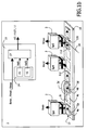
- Fig. 1 shows an embodiment 1 according to the invention which has a one dimensional array of magnetic bits 4a, 4b, 4c, 4d.
- the embodiment shown in Fig. 1a has a one dimensional array of magnetic bits 4a, 4b wherein each bit magnetic field 3a, 3b has a bit magnetization direction 5a, 5b.
- the magnetic bits 4a, 4b are located in an information layer 13 which is part of an information carrier 18.
- the information carrier 18 may be an integrated information carrier 18 in the system 1 or may be a removable information carrier 18.
- the Fig. 1a also shows a simplified representation of a sensor 2 which is shown to interact with the information layer 13 at three different locations Sp1 Sp2, Sp3.
- the sensor 2 comprises a magnetoresistive element 6 which has a stack of layers.
- the stack of layers includes a fixed magnetic layer 7 and a free magnetic layer 8.
- the fixed magnetic layer 7 has a fixed magnetization direction 9 which is considered not to be influenced by a nearby magnetic field.
- the free magnetic layer 8 has a magnetization axis 10 along which the free magnetic layer 8 retains two stable magnetization directions 11c. In the embodiment shown in Fig. 1 the magnetization axis 10 of the free magnetic layer 8 is perpendicular to the fixed magnetization direction 9.
- the sensor 2 interacts with a magnetic bit 4a which comprises a bit magnetic field 3a, also indicated as second bit magnetic field 3a.
- the second bit magnetic field 3a has a second bit magnetization direction 5a which is perpendicular to the magnetization axis 10 and which is parallel to the fixed magnetization direction 9.
- the presence of the second bit magnetization direction 5a rotates the free magnetization direction from one of the stable magnetization direction 11c to form an angle 12a with the magnetization axis 10.
- the second bit magnetic field 3a rotates the free magnetization direction 11c to the magnetization direction 11a where the angle 12a between the rotated free magnetization direction 11a and the magnetisation axis 10 is substantially 90 degrees.
- the free magnetization direction 11a points in the same direction as the fixed magnetization direction 9 which results in a low resistance value Rmin in the magnetoresistive element 6.
- the sensor 2 interacts with a magnetic bit 4b which comprises a bit magnetic field 3b, also indicated as first bit magnetic field 3b.
- the first bit magnetic field 3b has a first bit magnetization direction 5b which is parallel to the magnetization axis 10 and which is (in this embodiment) perpendicular to the fixed magnetization direction 9.
- the first bit magnetic field 3b forces the free magnetization direction 11c into the stable position 11b.
- the free magnetization direction 11b is perpendicular to the fixed magnetization direction 9 which results in an intermediate resistance value Rmid in the magnetoresistive element 6.
- the free magnetization direction 11c can be in any of the two stable magnetization directions parallel to the magnetization axis 10. In each of the two stable magnetization directions the free magnetization direction 11c will be perpendicular to the fixed magnetization direction 9.
- the resistance value in the magnetoresistive element 6 is the intermediate resistance value Rmid.
- the sensor 2 provides the sensed resistance value Rmin, Rmid to the read circuit 19 which comprises a reference circuit 14.
- the reference circuit 14 provides two reference levels Refl, Ref2 from reference generators 15, 16 which comprise reference magnetoresistive elements.
- the read circuit further comprises a comparator circuit 17 which compares the sensed resistance value Rmin, Rmid with at least one of the reference levels Ref1, Ref2.
- the comparator circuit 17 assigns the logical value L0, L1/2 to the resistance value provided by the magnetoresistive element 6 due to the magnetic bits 4a, 4b of the information layer 13.
- Fig. 1b shows an embodiment in which the magnetic field strength of the first bit magnetic field 3c is substantially zero. Furthermore, Fig. 1b comprises, next to the second bit magnetic field 3c also a further bit magnetic field 3d having a further magnetization direction 5d which is opposite to the second magnetization direction 5a.
- the sensor 2 comprises a low resistance value Rmin as indicated in Fig. 1a .
- the sensor 2 interacts with a bit location 4c not having a magnetic bit present.
- the free magnetization direction 11c of the sensor at the fourth sensor position Sp4 is undetermined and can be either of the two stable magnetization directions of the free magnetic layer 8. Because both the stable magnetization directions 11c of the free magnetic layer 8 are perpendicular to the magnetization axis 10, the resistance value in the magnetoresistive element 6 is always the intermediate resistance value Rmid.
- the sensor 2 interacts with a magnetic bit 4d which comprises a further bit magnetic field 3d which has a further bit magnetization direction 5d
- the further bit magnetization direction 5d is perpendicular to the magnetization axis 10 and points in the opposite direction compared to the second bit magnetization direction 5a.
- the presence of the further bit magnetic field 3d rotates the free magnetization direction from one of the stable magnetization direction 11c to form an angle 12d with the magnetization axis 10.
- the further bit magnetic field 3d rotates the free magnetization direction 11c to the magnetization direction 11d where the angle 12d between the rotated free magnetization direction 11d and the magnetization axis 10 is substantially 90 degrees.
- the free magnetization direction 11d points in the opposite direction compared to the fixed magnetization direction 9 which results in a high resistance value Rmax in the magnetoresistive element 6.
- the sensor 2 provides the sensed resistance value Rmax, Rmid, Rmin at each of the sensor positions Sp1, Sp4, Sp5 to the read circuit 19 where the comparator circuit 17 assigns the logical value L0, L1/2, L1 to the resistance value provided by the magnetoresistive element 6 due to the magnetic bit 4a, 4d or due to the bit location 4c of the information layer 13.
- the system shown in Fig. 1b In contrast with the system shown in Fig. 1a , which substantially describes a binary system having two logical values L0, L1/2, the system shown in Fig. 1b describes a tertiary system, having three logical values: L0, L1 /2, L1. To be able to discriminate between the three logical values L0, L1/2, L1, the read circuit 19 must have two reference levels Ref1, Ref2 as will be shown in Fig. 3 .
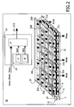
- Fig. 2 shows an embodiment 20 according to the invention which has an information carrier 23 which comprises a two dimensional pattern of magnetic bits 24a, 24c, 24d.
- the information carrier 23 may be an integrated information carrier 23 in the system 20 or may be a removable information carrier 23.
- Each magnetic bit 24a, 24c, 24d provides a second bit magnetic field (not shown) having a second bit magnetization direction 25a, 25d.
- the magnetic field strength of the first bit magnetic field is substantially zero, which is indicated by a bit location 24c without a magnetic bit present.
- the system 20 shown in Fig. 2 further comprises a sensor 22 which comprises a two dimensional array of magnetoresistive elements 26.
- Each magnetoresistive element 26 comprises a stack of layers having a fixed magnetic layer 7 and a free magnetic layer 8, identical to the magnetoresistive element 6 in Figs. 1a and 1b .
- the difference between the magnetoresistive element 6 shown in Figs. 1a and 1b and the magnetoresistive element 26 shown in Fig. 2 is that the magnetization axis 10 of the free magnetic layer 8 in the magnetoresistive element 26 is parallel to the fixed magnetization direction 9.
- the free magnetization direction is rotated from one of the two stable magnetization directions 21b, 21c to a magnetization direction 21 a which substantially points in the same direction as the second bit magnetization direction 25a.
- the rotated free magnetization direction 21 a is arranged perpendicular to the fixed magnetization direction 9 which results in an intermediate resistance value Rmid in the magnetoresistive element 26.
- the free magnetization direction can be any of the two stable magnetization directions 21b, 21c.
- the magnetoresistive element 26 comprises a low resistance value Rmin.
- the magnetoresistive element 26 comprises a high resistance value Rmax.
- the free magnetization direction 21 b, 21 c at the bit locations 24c may randomly be any of the two stable magnetization directions 21b, 21c and thus is undefined.
- the read circuit 19 is present which comprises the reference circuit 14.
- the reference circuit 14 provides two reference levels Refl, Ref2 based on reference magnetoresistive elements.
- the comparator circuit 17 assigns the logical value L0, L1/2 to the resistance value provided by the magnetoresistive element 26 due to the magnetic bit 24a or due to the bit location 24c of the information layer 13.
- the reference circuit 14 requires both reference levels Ref1, Ref2. Because the free magnetization direction at the bit location 24c may randomly be any of the two stable magnetization direction 21b, 21c (being Rmin, Rmax), the resistance value to which the comparator circuit 17 must assign the logical value L0 is both the low resistance value Rmin and the high resistance value Rmax. The resistance value to which the comparator circuit 17 must assign the logical value L1/2 is the intermediate resistance value Rmid.
- a first reference resistance value Ref1 must be between the low resistance value Rmin and the intermediate resistance value Rmid and a second reference resistance value Ref2 must be between the high resistance value Rmax and the intermediate resistance value Rmid. This is shown in more detail in Fig. 3 .
- the information carrier 22 may comprise a further magnetic bit 24d which has a further bit magnetization direction 25d.
- the further bit magnetization direction 25d is perpendicular to the magnetization axis 10 and points in the opposite direction compared to the second bit magnetization direction 25a.
- the presence of the further bit magnetic field rotates the free magnetization direction from one of the stable magnetization direction 21b, 21 c to the free magnetization direction 21d.
- the free magnetization direction 21d is arranged perpendicular to the fixed magnetization direction 9 which results in the intermediate resistance value Rmid which is identical to the intermediate resistance value Rmid which results from the free magnetization direction 21b.
- the comparator assigns, in the described configuration, the same logical value L1/2 to the bit location which comprises the further magnetization direction 25d.
- the rotation of the free magnetization directions must be altered, for example, using different field strength or changing the orientation of the second bit magnetization direction 25a and the further bit magnetization direction 25d.
- Fig. 3 shows the sensed resistance R in the magnetoresistive element 36 versus the bit magnetic field strength Hbit wherein the bit magnetization direction 25a is perpendicular to the magnetization axis 10.
- five identical magnetoresistive elements 36 are shown which each comprise a stack of layers having a fixed magnetic layer 7 and a free magnetic layer 8, identical to the magnetoresistive elements 6 and 26 in Figs. 1a , 1b and 2 .
- the magnetoresistive elements shown in Fig. 3 comprise a layer 32 which typically is a stabilizing layer for stabilizing the fixed magnetization direction 9 in the fixed magnetic layer 7.
- This layer comprises, for example, anti-ferromagnetic material which is magnetically coupled to the material in the fixed magnetic layer 7.
- the magnetization axis 10 of the free magnetic layers 8 in the magnetoresistive element 36 is parallel to the fixed magnetization direction 9.
- the magnetoresistive elements 36b and 36c show the two stable magnetization directions 21b, 21c of the free magnetic layer 8.
- the free magnetization direction 21b of the magnetoresistive element 36b points in the same direction as the fixed magnetization direction 9, which results in a low resistance value Rmin.
- the free magnetization direction 21 c of the magnetoresistive element 36c points in the opposite direction compared to the fixed magnetization direction 9, which results in a high resistance value Rmax.
- the free magnetization direction of the magnetoresistive element 36 can be in either stable magnetization direction 21b, 21 c.
- the magnetoresistive element 36a shows a rotated free magnetization direction 21 a which is perpendicular to the magnetic axis 10, which results in an intermediate resistance value Rmid.
- the rotated free magnetization direction 32a results from the interaction between the magnetoresistive element 36b and a magnetic bit 24a which has a magnetic field strength Hbit close to the minimum bit magnetic field strength Hbit min.
- the rotated free magnetization direction 32b results from the interaction between the magnetoresistive element 36c and a magnetic bit 24a which has a magnetic field strength Hbit close to the minimum bit magnetic field strength Hbit min .
- the lines 34a and 34b in the graph indicate the change in resistance in the magnetoresistive element 36 when the bit magnetic field strength of the magnetic bit 24a is increased.
- the reference resistance levels Ref1, Ref2 are indicated with the reference lines 33a and 33b.
- the graph shows that the resistance R in the magnetoresistive element 36 changes when the bit magnetic field strength increases. Furthermore, the graph shows that the resistance change must cross a reference level Ref1, Ref2 to discriminate, for example, the maximum resistance value Rmax from the intermediate resistance value Rmid. To enable the crossing of the reference level Ref1, Ref2, a minimum magnetic field strength Hbit min must be present at the magnetic bit 24a.
- a comparator circuit 17 Figs. 1 and 2
- the comparator circuit 17 can assign logical values L0, L1/2, L1 to the sensed resistance values as is indicated in Fig. 3 .
- both the maximum resistance value Rmax and the minimum resistance value Rmin represent the same state, being one without bit magnetic field or with a very weak bit magnetic field (for example stray fields).
- the comparator circuit 17 may then, for example, assign identical logical values, for example, L0 to both the maximum resistance value Rmax and the minimum resistance value Rmin.
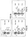
- Fig. 4 shows a summary of the preferred configurations of the magnetization directions as known from the prior art and as shown in Figs. 1 and 2 .
- Fig. 4a shows the configuration of the prior art in which the fixed magnetization direction 9 and the bit magnetization direction 42 both are parallel to the magnetization axis 10 of the magnetoresistive element 26.
- the magnetoresistive element 26 is identical to the magnetoresistive element 26 introduced in Fig. 2 .
- the state of the magnetoresistive element 26, when no magnetic bit is present, is undefined and may comprise either of the two stable magnetization directions 21c of the free magnetic layer 8.
- the resistance value Rmax, Rmin is not a unique parameter for identifying the presence of a magnetic bit. This illustrates the need for setting the free magnetic layer 8 before reading.
- Fig. 4b shows the configuration as is used in Fig. 2 .
- the state of the magnetoresistive element 26, when no magnetic bit is present is undefined and may comprise either of the two stable magnetization directions 21 c of the free magnetic layer 8.
- the bit magnetization direction 25a, 25d of the magnetic bits 24a, 24d are perpendicular to the magnetization axis 10.
- the free magnetization direction 21 a, 21 d will be rotated by the bit magnetic field which results in the intermediate resistance value Rmid.
- the resistance value Rmid with a magnetic bit 24a, 24d present can be discriminated from the resistance value Rmax, Rmin without a magnetic bit present, which clearly omits the need for setting the free magnetic layer before reading.
- Fig. 4c shows the configuration as used in Fig. 1 in which the fixed magnetization direction 9 is perpendicular to the magnetization axis 10.
- the state of the magnetoresistive element 6, when no magnetic bit is present is defined, being the intermediate resistance value Rmid.
- Rmid the intermediate resistance value
- the resistance value will then be either the maximum resistance value Rmax when the rotated free magnetization direction 11d is pointing in the opposite direction compared to the fixed magnetization direction 9 or the resistance value will be the minimum resistance value Rmin when the rotated free magnetization direction 11a is pointing in the same direction as the fixed magnetization direction 9.
- a benefit of this embodiment is that it can distinguish between two magnetic bits 4a, 4d with opposite magnetization directions 5a, 5d enabling a tertiary system which comprises three logical values.
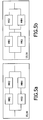
- Fig. 5 shows some embodiments of reference generators 15,16 according to the invention.
- Figs. 5a and 5b show voltage reference generators 15, 16 which each comprise 4 reference magnetoresistive elements MR1, MR2, MR3, MR4.
- Fig. 5c shows a current comparator scheme in which a current mirror CM1, CM2 is used to provide the reference levels Ref1, Ref2.
- Voltage reference generators are known from US 6,445,612 .
- four reference magnetoresistive elements are used to provide a midpoint reference for MRAM memory cells in a configuration comparable to the configurations shown in Figs. 5a and 5b .
- Fig. 5a shows four reference magnetoresistive elements MR1, MR2, MR3, MR4 where a first reference magnetoresistive element MR1 connected in series with a second reference magnetoresistive element MR2 is connected parallel to a third reference magnetoresistive element MR3 connected in series with a fourth reference magnetoresistive element MR4.
- the reference magnetoresistive elements MR1, MR2, MR3, MR4 can be programmed in such a manner that they either represent a resistance value between the maximum resistance value Rmax and the intermediate resistance value Rmid or represent a resistance value between the minimum resistance value Rmin and the intermediate resistance value Rmid.
- the complete circuit shown in Fig. 5a represents a resistance value close to Rmin plus 25% of (Rmax-Rmin).
- This configuration may, for example, be used as first reference level Ref1 in the reference circuit 14 (see Figs. 1 and 2 ).
- the complete circuit shown in Fig. 5a represents a resistance value close to Rmin plus 75% of (Rmax-Rmin).
- This configuration may, for example, be used as second reference level Ref2 in the reference circuit 14.
- Fig. 5b shows four reference magnetoresistive elements MR1, MR2, MR3, MR4 where the first reference magnetoresistive element MR1 connected parallel to the third reference magnetoresistive element MR3 is connected in series with the second reference magnetoresistive element MR2 connected parallel to the fourth reference magnetoresistive element.
- the magnetoresistive elements MR1, MR2, MR3, MR4 can be programmed in such a manner that they either represent a resistance value between the maximum resistance value Rmax and the intermediate resistance value Rmid or represent a resistance value between the minimum resistance value Rmin and the intermediate resistance value Rmid.
- the complete circuit shown in Fig. 5a represents a resistance value of Rmin plus 20% of (Rmax-Rmin).
- this configuration may, for example, be used as first reference level Ref1 in the reference circuit 14 (see Figs. 1 and 2 ).
- the complete circuit shown in Fig. 5a represents a resistance value of Rmin plus 70% of (Rmax-Rmin).
- This configuration may, for example, be used as second reference level Ref2 in the reference circuit 14.
- Fig. 5c shows a current comparator scheme.
- Current comparator circuits are known from US 6,621,729 .
- a current comparator circuit is shown using two reference magnetoresistive elements to provide a midpoint reference for MRAM memory cells in a configuration comparable to the configurations shown in Fig. 5c .
- a reference circuit 14 shown in Fig. 5c comprises two reference generators 15, 16 for generating the two reference levels Ref1, Ref2.
- the reference generators 15, 16 both comprise a parallel arrangement of four reference magnetoresistive element MR1 to MR8 and a current mirror CM1, CM2 with a current ratio of 4:1 to scale the current back to a reference current. This enables a comparison between the read current of the magnetoresistive element and the reference current.
- the reference magnetoresistive elements MR1 to MR8 can be programmed in such a manner that, for example, the first current mirror CM1 represents a current for distinguishing between the maximum resistance value Rmax and the intermediate resistance value Rmid and that, for example, a second current mirror CM2 represents a current for distinguishing between the minimum resistance value Rmin and the intermediate resistance value Rmid.
- These configurations may, for example, be used as the first reference level Ref1 and the second reference level Ref2 in the reference circuit 14.
- any reference signs placed between parentheses shall not be construed as limiting the claim.
- Use of the verb "comprise” and its conjugations does not exclude the presence of elements or steps other than those stated in a claim.
- the article "a” or “an” preceding an element does not exclude the presence of a plurality of such elements.
- the invention may be implemented by means of hardware comprising several distinct elements, and by means of a suitably programmed computer. In the device claim enumerating several means, several of these means may be embodied by one and the same item of hardware. The mere fact that certain measures are recited in mutually different dependent claims does not indicate that a combination of these measures cannot be used to advantage.
Landscapes
- Engineering & Computer Science (AREA)
- Computer Hardware Design (AREA)
- Hall/Mr Elements (AREA)
- Measuring Magnetic Variables (AREA)
- Mram Or Spin Memory Techniques (AREA)
Claims (13)
- Magnetisches Speichersystem (1, 20), welches eine Informationsschicht (13), welche keinen Teil eines magnetischen Tunnelkontakts, kurz MTJ, bildet, welche ein Teil eines integrierten oder entfernbar angebrachten Informationsträgers (18) ist, und einen Sensor (2, 22) zum Kooperieren mit der Informationsschicht (13) aufweist,
wobei die Informationsschicht (13) ein Muster von magnetischen Bits (4a, 4b, 4c, 4d, 24a, 24c, 24d) aufweist, welche ein Feld von Bit-Positionen bilden, wobei ein Bit-Magnetfeld (3a, 3b, 3c, 3d) bei einer Bit-Position einen logischen Wert ausgewählt von einer Gruppe von drei logischen Werten (L0, L1/2, L1) repräsentiert, wobei das Bit-Magnetfeld (3a, 3b, 3c, 3d) eine Bit-Magnetfeldstärke und eine Bit-Magnetisierungsrichtung (5a, 5b, 5d, 25a, 25d) hat,
wobei der Sensor (2, 22) ein magnetoresistives Element (6, 26) aufweist, welches einen Stapel von Schichten einschließlich einer fixen magnetischen Schicht (7) und einer freien magnetischen Schicht (8) aufweist, wobei die fixe magnetische Schicht (7) eine fixe Magnetisierungsrichtung (9) hat und wobei die freie magnetische Schicht (8) eine Magnetisierungsachse (10) hat, entlang welcher die freie magnetische Schicht eine freie Magnetisierungsrichtung (11b, 11c, 21b, 21c) behält,
dadurch gekennzeichnet, dass
ein erstes Bit-Magnetfeld (3b, 3c) bei einer der Bit-Positionen einen ersten logischen Wert ausgewählt von der Gruppe von drei logischen Werten (L0, L1/2, L1) dadurch repräsentiert, dass ein erster Widerstandswert (Rmax, Rmid, Rmin) in einem magnetoresistiven Element (6, 26) dadurch bedingt, dass die freie Magnetisierungsrichtung (11c, 11b, 21b, 21c) im Wesentlichen parallel zu der Magnetisierungsachse (10) ist, bereitgestellt ist, und dadurch, dass ein zweites Bit-Magnetfeld (3a, 3d) bei einer der Bit-Positionen einen zweiten logischen Wert ausgewählt von der Gruppe von drei logischen Werten (L0, L1/2, L1) dadurch repräsentiert, dass ein zweiter Widerstandswert (Rmax, Rmid, Rmin) in einem magnetoresistiven Element (6, 26) bedingt durch die freie Magnetisierungsrichtung- (11a, 11d, 21a, 21d) -Rotation bereitgestellt ist, welche zu einem Winkel (12a, 12d, 27) zwischen der Magnetisierungsachse (10) der freien magnetischen Schicht und der freien Magnetisierungsrichtung führt. - System (1, 20) gemäß Anspruch 1, wobei das erste Bit-Magnetfeld (3c) eine erste Magnetfeldsstärke hat, welche im Wesentlichen Null ist.
- System (1, 20) gemäß Anspruch 1 oder 2, wobei das zweite Bit-Magnetfeld (3a, 3d) eine zweite Magnetisierungsrichtung (5a, 5d, 25a, 25d) hat, welche im Wesentlichen senkrecht zu der Magnetisierungsachse (10) ist.
- System (1, 20) gemäß Ansprüchen 1, 2 oder 3, wobei ein weiteres Bit-Magnetfeld (3d) bei einer der Bit-Positionen einen weiteren logischen Wert (L1) dadurch repräsentiert, dass ein weiterer Widerstandswert (Rmax) in dem magnetoresistiven Element (6, 26) bedingt dadurch, dass die freie Magnetisierungsrichtung (11d, 21d) einen weiteren Winkel (12d) mit der Magnetisierungsachse (10) hat, bereitgestellt ist, wobei der weitere Winkel (12d) verschieden von dem Winkel (12a, 27) ist, welcher zu dem zweiten logischen Wert (L0) führt.
- System (1, 20) gemäß Ansprüchen 1, 2, 3 oder 4, wobei die fixe Magnetisierungsrichtung (9) im Wesentlichen parallel zu der Magnetisierungsachse (10) der freien magnetischen Schicht (8) ist.
- System (1, 20) gemäß Ansprüchen 1, 2, 3 oder 4, wobei die fixe Magnetisierungsrichtung (9) im Wesentlichen senkrecht zu der Magnetisierungsachse (10) der freien magnetischen Schicht (8) ist.
- System (1, 20) gemäß Anspruch 1, wobei das System (1, 20) eine Referenzschaltung (14) aufweist, wobei die Referenzschaltung (14) zumindest einen Referenzpegel (Ref1, Ref2) basierend auf Referenz-magnetoresistiven Elementen bereitstellt zum Unterscheiden des ersten Widerstandswerts (Rmax, Rmid, Rmin) von dem zweiten Widerstandswert (Rmax, Rmid, Rmin).
- System (1, 20) gemäß Anspruch 7, wobei die Referenzschaltung (14) zumindest einen zweiten Referenzpegel (Ref1, Ref2) basierend auf Referenz-magnetoresistiven Elementen bereitstellt zum Unterscheiden von Widerstandswerten, welche zwischen zwei Referenzpegeln (Ref1, Ref2) liegen.
- System (1, 20) gemäß einem der vorherigen Ansprüche, wobei das Bit-Magnetfeld (3a, 3b, 3c, 3d) bei einer der Bit-Positionen dadurch bereitgestellt ist, dass magnetisiertes Material (4a, 4b, 4d, 24a, 24d) bei der einen der Bit-Positionen vorhanden ist oder nicht vorhanden ist.
- System (1, 20) gemäß einem der vorherigen Ansprüche, wobei der Sensor (22) ein zweidimensionales Feld von magnetoresistiven Elementen (26) aufweist.
- Informationsträger (18, 23) zur Benutzung in dem System (1, 20) von Anspruch 1, wobei der Informationsträger (18, 22) eine Informationsschicht (13) aufweist, welche ein Muster von magnetischen Bits (4a, 4b, 4c, 4d, 24a, 24c, 24d) aufweist, welche ein Feld von Bit-Positionen bilden, wobei ein Bit-Magnetfeld (3a, 3b, 3c, 3d) bei einer Bit-Position einen logischen Wert ausgewählt von einer Gruppe von drei logischen Werten (L0, L1/2, L1) repräsentiert, wobei das Bit-Magnetfeld (3a, 3b, 3c, 3d) eine Bit-Magnetfeldstärke und eine Bit-Magnetisierungsrichtung (5a, 5b, 5d, 25a, 25d) hat, dadurch gekennzeichnet, dass
ein erstes Bit-Magnetfeld (3b, 3c) bei einer der Bit-Positionen einen ersten logischen Wert ausgewählt von einer Gruppe von drei logischen Werten (L0, L1/2, L1) dadurch repräsentiert, dass ein erster Widerstandswert (Rmax, Rmid, Rmin) in einem magnetoresistiven Element (6, 26), welches keinen Teil der Informationsschicht bildet, dadurch bedingt, dass die freie Magnetisierungsrichtung (11c, 11d, 21b, 21c) im Wesentlichen parallel zu der Magnetisierungsachse (10) ist, bereitgestellt ist, und dadurch, dass ein zweites Bit-Magnetfeld (3a, 3d) bei einer der Bit-Positionen einen zweiten logischen Wert ausgewählt von einer Gruppe von drei logischen Werten (L0, L1/2, L1) dadurch repräsentiert, dass ein zweiter Widerstandswert (Rmax, Rmid, Rmin) in dem magnetoresistiven Element (6, 26) bedingt durch die freie Magnetisierungsrichtung- (11a, 11d, 21a, 21d) -Rotation bereitgestellt ist, welche zu einem Winkel (12a, 12d, 27) zwischen der Magnetisierungsachse (10) der freien magnetischen Schicht und der freien Magnetisierungsrichtung führt, und dadurch, dass ein weiteres Bit-Magnetfeld (3d) bei einer der Bit-Positionen einen weiteren logischen Wert (L1) dadurch repräsentiert, dass ein weiterer Widerstandswert (Rmax) in einem magnetoresistiven Element (6, 26), welches keinen Teil der Informationsschicht bildet, bedingt durch die freie Magnetisierungsrichtung- (11d, 21d) - Rotation bereitgestellt ist, welche zu einem weiteren Winkel (12d) zwischen der Magnetisierungsachse (10) der freien magnetischen Schicht und der freien Magnetisierungsrichtung führt, wobei der weitere Winkel (12d) verschieden von dem Winkel (12a, 27) ist, welcher zu dem zweiten logischen Wert (L0) führt. - Leseschaltung (19) zur Benutzung in dem System (1, 20) von Anspruch 1 zum Lesen eines logischen Wertes von einem Sensor (2, 22), welcher ein magnetoresistives Element (6, 26) aufweist, wobei die Leseschaltung (19) eine Referenzschaltung (14) zum Bereitstellen zumindest zweier Referenzpegel (Ref1, Ref2) basierend auf Referenz-magnetoresistiven Elementen aufweist und wobei der logische Wert ausgewählt von einer Gruppe von drei logischen Werten (L0, L1/2, L1) dadurch gelesen wird, dass ein Widerstandswert (Rmax, Rmid, Rmin) in dem magnetoresistiven Element (6, 26) mit den zumindest zwei Referenzpegeln (Ref1, Ref2) verglichen wird.
- Leseschaltung (19) gemäß Anspruch 12, welche zwei Referenzpegel (Ref1, Ref2) hat, wobei ein Referenzwiderstandsbereich zwischen den zwei Referenzpegeln (Ref1, Ref2) liegt und wobei ein logischer Wert ausgewählt von einer Gruppe von drei logischen Werten (L0, L1/2, L1) gelesen wird, wenn der Widerstandswert innerhalb des Referenzwiderstandsbereiches ist und wobei ein zweiter logischer Wert ausgewählt von einer Gruppe von drei logischen Werten (L0, L1/2, L1) gelesen wird, wenn der Widerstandswert außerhalb des Referenzwiderstandsbereichs ist.
Priority Applications (1)
| Application Number | Priority Date | Filing Date | Title |
|---|---|---|---|
| EP06710706A EP1844472B1 (de) | 2005-01-24 | 2006-01-19 | Magnetisches speichersystem unter verwendung von mram-abtaster |
Applications Claiming Priority (3)
| Application Number | Priority Date | Filing Date | Title |
|---|---|---|---|
| EP05100427 | 2005-01-24 | ||
| PCT/IB2006/050208 WO2006077553A1 (en) | 2005-01-24 | 2006-01-19 | Magnetic memory system using mram-sensor |
| EP06710706A EP1844472B1 (de) | 2005-01-24 | 2006-01-19 | Magnetisches speichersystem unter verwendung von mram-abtaster |
Publications (2)
| Publication Number | Publication Date |
|---|---|
| EP1844472A1 EP1844472A1 (de) | 2007-10-17 |
| EP1844472B1 true EP1844472B1 (de) | 2012-01-11 |
Family
ID=36591362
Family Applications (1)
| Application Number | Title | Priority Date | Filing Date |
|---|---|---|---|
| EP06710706A Expired - Lifetime EP1844472B1 (de) | 2005-01-24 | 2006-01-19 | Magnetisches speichersystem unter verwendung von mram-abtaster |
Country Status (7)
| Country | Link |
|---|---|
| US (1) | US7791937B2 (de) |
| EP (1) | EP1844472B1 (de) |
| JP (1) | JP2008529195A (de) |
| CN (1) | CN101167136B (de) |
| AT (1) | ATE541295T1 (de) |
| TW (1) | TW200632904A (de) |
| WO (1) | WO2006077553A1 (de) |
Families Citing this family (3)
| Publication number | Priority date | Publication date | Assignee | Title |
|---|---|---|---|---|
| DE102011120972A1 (de) * | 2011-12-13 | 2013-06-13 | Giesecke & Devrient Gmbh | Verfahren und Vorrichtung zur Prüfung von Wertdokumenten |
| US8848431B2 (en) | 2012-07-30 | 2014-09-30 | Honeywell International Inc. | Magnetic field sensing using magnetoresistive random access memory (MRAM) cells |
| US10763425B1 (en) | 2019-05-30 | 2020-09-01 | Honeywell International Inc. | Magnetic tunnel junction based programmable memory cell |
Family Cites Families (11)
| Publication number | Priority date | Publication date | Assignee | Title |
|---|---|---|---|---|
| US5966323A (en) * | 1997-12-18 | 1999-10-12 | Motorola, Inc. | Low switching field magnetoresistive tunneling junction for high density arrays |
| US5982660A (en) * | 1998-08-27 | 1999-11-09 | Hewlett-Packard Company | Magnetic memory cell with off-axis reference layer orientation for improved response |
| US6215695B1 (en) * | 1998-12-08 | 2001-04-10 | Canon Kabushiki Kaisha | Magnetoresistance element and magnetic memory device employing the same |
| JP2001084756A (ja) * | 1999-09-17 | 2001-03-30 | Sony Corp | 磁化駆動方法、磁気機能素子および磁気装置 |
| US6873547B1 (en) * | 2001-02-23 | 2005-03-29 | Read Rite Corporation | High capacity MRAM memory array architecture |
| US6654278B1 (en) * | 2002-07-31 | 2003-11-25 | Motorola, Inc. | Magnetoresistance random access memory |
| US20070140099A1 (en) | 2002-10-03 | 2007-06-21 | Lenssen Kars-Michiel H | Read-only magnetic memory device mrom |
| JP2004153181A (ja) * | 2002-10-31 | 2004-05-27 | Toshiba Corp | 磁気抵抗効果素子および磁気メモリ |
| JP2004280892A (ja) * | 2003-03-13 | 2004-10-07 | Toshiba Corp | 半導体記憶装置及びその制御方法 |
| JP2006120824A (ja) * | 2004-10-21 | 2006-05-11 | Renesas Technology Corp | 磁気記憶装置 |
| US7321507B2 (en) * | 2005-11-21 | 2008-01-22 | Magic Technologies, Inc. | Reference cell scheme for MRAM |
-
2006
- 2006-01-19 US US11/814,674 patent/US7791937B2/en not_active Expired - Fee Related
- 2006-01-19 WO PCT/IB2006/050208 patent/WO2006077553A1/en not_active Ceased
- 2006-01-19 AT AT06710706T patent/ATE541295T1/de active
- 2006-01-19 CN CN2006800028867A patent/CN101167136B/zh not_active Expired - Fee Related
- 2006-01-19 JP JP2007551796A patent/JP2008529195A/ja not_active Withdrawn
- 2006-01-19 EP EP06710706A patent/EP1844472B1/de not_active Expired - Lifetime
- 2006-01-20 TW TW095102266A patent/TW200632904A/zh unknown
Also Published As
| Publication number | Publication date |
|---|---|
| US20080316801A1 (en) | 2008-12-25 |
| TW200632904A (en) | 2006-09-16 |
| WO2006077553A1 (en) | 2006-07-27 |
| US7791937B2 (en) | 2010-09-07 |
| CN101167136B (zh) | 2011-01-19 |
| JP2008529195A (ja) | 2008-07-31 |
| ATE541295T1 (de) | 2012-01-15 |
| EP1844472A1 (de) | 2007-10-17 |
| CN101167136A (zh) | 2008-04-23 |
Similar Documents
| Publication | Publication Date | Title |
|---|---|---|
| KR100898875B1 (ko) | 스케일링 가능한 mram 소자에의 기록 | |
| US7881099B2 (en) | Multibit magnetic random access memory device | |
| EP1074992B1 (de) | Magnetische Direktzugriffspeicheranordnung | |
| US7453747B2 (en) | Active compensation for operating point drift in MRAM write operation | |
| US6205053B1 (en) | Magnetically stable magnetoresistive memory element | |
| TW200410247A (en) | Magnetoresistance random access memory | |
| JP2000030434A (ja) | 磁気メモリセル | |
| JP2007503670A (ja) | 多状態磁気ランダムアクセスメモリセル | |
| US20010043488A1 (en) | Magnetoresistive memory having elevated interference immunity | |
| US7313043B2 (en) | Magnetic Memory Array | |
| US20060171196A1 (en) | Method for writing to magnetoresistive memory cells and magnetoresistive memory which can be written to by the method | |
| US7102477B2 (en) | Magnetic element with switchable domain structure | |
| US7453740B2 (en) | Method and apparatus for initializing reference cells of a toggle switched MRAM device | |
| JP2009004086A (ja) | 磁気メモリセルのアレイ、磁気メモリセル書き込み電流選択方法および磁気抵抗アクセスメモリ | |
| US7224634B2 (en) | Hardware security device for magnetic memory cells | |
| EP1844472B1 (de) | Magnetisches speichersystem unter verwendung von mram-abtaster | |
| JP2004508698A (ja) | 高密度巨大磁気抵抗メモリセル | |
| KR100563423B1 (ko) | 자성 메모리, 자성 메모리 어레이, 자성 메모리로의 기록 방법 및 자성 메모리로부터의 판독 방법 | |
| US6836429B2 (en) | MRAM having two write conductors | |
| US20060067115A1 (en) | MRAM with improved storage and read out characteristics | |
| JP2007514256A (ja) | 磁気メモリ用のデータ保持インジケータ | |
| US7123507B2 (en) | Using permanent magnets in MRAM to assist write operation | |
| JP2005122885A (ja) | メモリセルを読み取るための方法 |
Legal Events
| Date | Code | Title | Description |
|---|---|---|---|
| PUAI | Public reference made under article 153(3) epc to a published international application that has entered the european phase |
Free format text: ORIGINAL CODE: 0009012 |
|
| 17P | Request for examination filed |
Effective date: 20070824 |
|
| AK | Designated contracting states |
Kind code of ref document: A1 Designated state(s): AT BE BG CH CY CZ DE DK EE ES FI FR GB GR HU IE IS IT LI LT LU LV MC NL PL PT RO SE SI SK TR |
|
| DAX | Request for extension of the european patent (deleted) | ||
| 17Q | First examination report despatched |
Effective date: 20080428 |
|
| GRAP | Despatch of communication of intention to grant a patent |
Free format text: ORIGINAL CODE: EPIDOSNIGR1 |
|
| GRAS | Grant fee paid |
Free format text: ORIGINAL CODE: EPIDOSNIGR3 |
|
| GRAA | (expected) grant |
Free format text: ORIGINAL CODE: 0009210 |
|
| AK | Designated contracting states |
Kind code of ref document: B1 Designated state(s): AT BE BG CH CY CZ DE DK EE ES FI FR GB GR HU IE IS IT LI LT LU LV MC NL PL PT RO SE SI SK TR |
|
| REG | Reference to a national code |
Ref country code: GB Ref legal event code: FG4D |
|
| REG | Reference to a national code |
Ref country code: CH Ref legal event code: EP |
|
| REG | Reference to a national code |
Ref country code: AT Ref legal event code: REF Ref document number: 541295 Country of ref document: AT Kind code of ref document: T Effective date: 20120115 |
|
| REG | Reference to a national code |
Ref country code: IE Ref legal event code: FG4D |
|
| REG | Reference to a national code |
Ref country code: DE Ref legal event code: R096 Ref document number: 602006026981 Country of ref document: DE Effective date: 20120315 |
|
| PGFP | Annual fee paid to national office [announced via postgrant information from national office to epo] |
Ref country code: FR Payment date: 20120216 Year of fee payment: 7 |
|
| REG | Reference to a national code |
Ref country code: NL Ref legal event code: VDEP Effective date: 20120111 |
|
| PG25 | Lapsed in a contracting state [announced via postgrant information from national office to epo] |
Ref country code: SI Free format text: LAPSE BECAUSE OF FAILURE TO SUBMIT A TRANSLATION OF THE DESCRIPTION OR TO PAY THE FEE WITHIN THE PRESCRIBED TIME-LIMIT Effective date: 20120111 |
|
| PGFP | Annual fee paid to national office [announced via postgrant information from national office to epo] |
Ref country code: DE Payment date: 20120123 Year of fee payment: 7 |
|
| LTIE | Lt: invalidation of european patent or patent extension |
Effective date: 20120111 |
|
| PGFP | Annual fee paid to national office [announced via postgrant information from national office to epo] |
Ref country code: GB Payment date: 20120224 Year of fee payment: 7 |
|
| PG25 | Lapsed in a contracting state [announced via postgrant information from national office to epo] |
Ref country code: NL Free format text: LAPSE BECAUSE OF FAILURE TO SUBMIT A TRANSLATION OF THE DESCRIPTION OR TO PAY THE FEE WITHIN THE PRESCRIBED TIME-LIMIT Effective date: 20120111 Ref country code: BE Free format text: LAPSE BECAUSE OF FAILURE TO SUBMIT A TRANSLATION OF THE DESCRIPTION OR TO PAY THE FEE WITHIN THE PRESCRIBED TIME-LIMIT Effective date: 20120111 Ref country code: LT Free format text: LAPSE BECAUSE OF FAILURE TO SUBMIT A TRANSLATION OF THE DESCRIPTION OR TO PAY THE FEE WITHIN THE PRESCRIBED TIME-LIMIT Effective date: 20120111 Ref country code: IS Free format text: LAPSE BECAUSE OF FAILURE TO SUBMIT A TRANSLATION OF THE DESCRIPTION OR TO PAY THE FEE WITHIN THE PRESCRIBED TIME-LIMIT Effective date: 20120511 Ref country code: BG Free format text: LAPSE BECAUSE OF FAILURE TO SUBMIT A TRANSLATION OF THE DESCRIPTION OR TO PAY THE FEE WITHIN THE PRESCRIBED TIME-LIMIT Effective date: 20120411 |
|
| PG25 | Lapsed in a contracting state [announced via postgrant information from national office to epo] |
Ref country code: FI Free format text: LAPSE BECAUSE OF FAILURE TO SUBMIT A TRANSLATION OF THE DESCRIPTION OR TO PAY THE FEE WITHIN THE PRESCRIBED TIME-LIMIT Effective date: 20120111 Ref country code: MC Free format text: LAPSE BECAUSE OF NON-PAYMENT OF DUE FEES Effective date: 20120131 Ref country code: GR Free format text: LAPSE BECAUSE OF FAILURE TO SUBMIT A TRANSLATION OF THE DESCRIPTION OR TO PAY THE FEE WITHIN THE PRESCRIBED TIME-LIMIT Effective date: 20120412 Ref country code: LV Free format text: LAPSE BECAUSE OF FAILURE TO SUBMIT A TRANSLATION OF THE DESCRIPTION OR TO PAY THE FEE WITHIN THE PRESCRIBED TIME-LIMIT Effective date: 20120111 Ref country code: PL Free format text: LAPSE BECAUSE OF FAILURE TO SUBMIT A TRANSLATION OF THE DESCRIPTION OR TO PAY THE FEE WITHIN THE PRESCRIBED TIME-LIMIT Effective date: 20120111 Ref country code: PT Free format text: LAPSE BECAUSE OF FAILURE TO SUBMIT A TRANSLATION OF THE DESCRIPTION OR TO PAY THE FEE WITHIN THE PRESCRIBED TIME-LIMIT Effective date: 20120511 |
|
| REG | Reference to a national code |
Ref country code: CH Ref legal event code: PL |
|
| REG | Reference to a national code |
Ref country code: AT Ref legal event code: MK05 Ref document number: 541295 Country of ref document: AT Kind code of ref document: T Effective date: 20120111 |
|
| PG25 | Lapsed in a contracting state [announced via postgrant information from national office to epo] |
Ref country code: CY Free format text: LAPSE BECAUSE OF FAILURE TO SUBMIT A TRANSLATION OF THE DESCRIPTION OR TO PAY THE FEE WITHIN THE PRESCRIBED TIME-LIMIT Effective date: 20120111 |
|
| REG | Reference to a national code |
Ref country code: IE Ref legal event code: MM4A |
|
| PG25 | Lapsed in a contracting state [announced via postgrant information from national office to epo] |
Ref country code: LI Free format text: LAPSE BECAUSE OF NON-PAYMENT OF DUE FEES Effective date: 20120131 Ref country code: DK Free format text: LAPSE BECAUSE OF FAILURE TO SUBMIT A TRANSLATION OF THE DESCRIPTION OR TO PAY THE FEE WITHIN THE PRESCRIBED TIME-LIMIT Effective date: 20120111 Ref country code: CZ Free format text: LAPSE BECAUSE OF FAILURE TO SUBMIT A TRANSLATION OF THE DESCRIPTION OR TO PAY THE FEE WITHIN THE PRESCRIBED TIME-LIMIT Effective date: 20120111 Ref country code: CH Free format text: LAPSE BECAUSE OF NON-PAYMENT OF DUE FEES Effective date: 20120131 Ref country code: RO Free format text: LAPSE BECAUSE OF FAILURE TO SUBMIT A TRANSLATION OF THE DESCRIPTION OR TO PAY THE FEE WITHIN THE PRESCRIBED TIME-LIMIT Effective date: 20120111 Ref country code: EE Free format text: LAPSE BECAUSE OF FAILURE TO SUBMIT A TRANSLATION OF THE DESCRIPTION OR TO PAY THE FEE WITHIN THE PRESCRIBED TIME-LIMIT Effective date: 20120111 Ref country code: SE Free format text: LAPSE BECAUSE OF FAILURE TO SUBMIT A TRANSLATION OF THE DESCRIPTION OR TO PAY THE FEE WITHIN THE PRESCRIBED TIME-LIMIT Effective date: 20120111 |
|
| PLBE | No opposition filed within time limit |
Free format text: ORIGINAL CODE: 0009261 |
|
| STAA | Information on the status of an ep patent application or granted ep patent |
Free format text: STATUS: NO OPPOSITION FILED WITHIN TIME LIMIT |
|
| PG25 | Lapsed in a contracting state [announced via postgrant information from national office to epo] |
Ref country code: SK Free format text: LAPSE BECAUSE OF FAILURE TO SUBMIT A TRANSLATION OF THE DESCRIPTION OR TO PAY THE FEE WITHIN THE PRESCRIBED TIME-LIMIT Effective date: 20120111 Ref country code: IT Free format text: LAPSE BECAUSE OF FAILURE TO SUBMIT A TRANSLATION OF THE DESCRIPTION OR TO PAY THE FEE WITHIN THE PRESCRIBED TIME-LIMIT Effective date: 20120111 |
|
| 26N | No opposition filed |
Effective date: 20121012 |
|
| PG25 | Lapsed in a contracting state [announced via postgrant information from national office to epo] |
Ref country code: IE Free format text: LAPSE BECAUSE OF NON-PAYMENT OF DUE FEES Effective date: 20120119 Ref country code: AT Free format text: LAPSE BECAUSE OF FAILURE TO SUBMIT A TRANSLATION OF THE DESCRIPTION OR TO PAY THE FEE WITHIN THE PRESCRIBED TIME-LIMIT Effective date: 20120111 |
|
| REG | Reference to a national code |
Ref country code: DE Ref legal event code: R097 Ref document number: 602006026981 Country of ref document: DE Effective date: 20121012 |
|
| PG25 | Lapsed in a contracting state [announced via postgrant information from national office to epo] |
Ref country code: ES Free format text: LAPSE BECAUSE OF FAILURE TO SUBMIT A TRANSLATION OF THE DESCRIPTION OR TO PAY THE FEE WITHIN THE PRESCRIBED TIME-LIMIT Effective date: 20120422 |
|
| GBPC | Gb: european patent ceased through non-payment of renewal fee |
Effective date: 20130119 |
|
| REG | Reference to a national code |
Ref country code: FR Ref legal event code: ST Effective date: 20130930 |
|
| PG25 | Lapsed in a contracting state [announced via postgrant information from national office to epo] |
Ref country code: DE Free format text: LAPSE BECAUSE OF NON-PAYMENT OF DUE FEES Effective date: 20130801 |
|
| REG | Reference to a national code |
Ref country code: DE Ref legal event code: R119 Ref document number: 602006026981 Country of ref document: DE Effective date: 20130801 |
|
| PG25 | Lapsed in a contracting state [announced via postgrant information from national office to epo] |
Ref country code: FR Free format text: LAPSE BECAUSE OF NON-PAYMENT OF DUE FEES Effective date: 20130131 Ref country code: GB Free format text: LAPSE BECAUSE OF NON-PAYMENT OF DUE FEES Effective date: 20130119 |
|
| PG25 | Lapsed in a contracting state [announced via postgrant information from national office to epo] |
Ref country code: TR Free format text: LAPSE BECAUSE OF FAILURE TO SUBMIT A TRANSLATION OF THE DESCRIPTION OR TO PAY THE FEE WITHIN THE PRESCRIBED TIME-LIMIT Effective date: 20120111 |
|
| PG25 | Lapsed in a contracting state [announced via postgrant information from national office to epo] |
Ref country code: LU Free format text: LAPSE BECAUSE OF NON-PAYMENT OF DUE FEES Effective date: 20120119 |
|
| PG25 | Lapsed in a contracting state [announced via postgrant information from national office to epo] |
Ref country code: HU Free format text: LAPSE BECAUSE OF FAILURE TO SUBMIT A TRANSLATION OF THE DESCRIPTION OR TO PAY THE FEE WITHIN THE PRESCRIBED TIME-LIMIT Effective date: 20060119 |