EP1821347A2 - Light emitting device having vertical structure and method for manufacturing the same - Google Patents
Light emitting device having vertical structure and method for manufacturing the same Download PDFInfo
- Publication number
- EP1821347A2 EP1821347A2 EP07250583A EP07250583A EP1821347A2 EP 1821347 A2 EP1821347 A2 EP 1821347A2 EP 07250583 A EP07250583 A EP 07250583A EP 07250583 A EP07250583 A EP 07250583A EP 1821347 A2 EP1821347 A2 EP 1821347A2
- Authority
- EP
- European Patent Office
- Prior art keywords
- layer
- light emitting
- electrode
- emitting device
- semiconductor layer
- Prior art date
- Legal status (The legal status is an assumption and is not a legal conclusion. Google has not performed a legal analysis and makes no representation as to the accuracy of the status listed.)
- Granted
Links
Images



Classifications
-
- H—ELECTRICITY
- H10—SEMICONDUCTOR DEVICES; ELECTRIC SOLID-STATE DEVICES NOT OTHERWISE PROVIDED FOR
- H10H—INORGANIC LIGHT-EMITTING SEMICONDUCTOR DEVICES HAVING POTENTIAL BARRIERS
- H10H20/00—Individual inorganic light-emitting semiconductor devices having potential barriers, e.g. light-emitting diodes [LED]
- H10H20/80—Constructional details
- H10H20/83—Electrodes
- H10H20/832—Electrodes characterised by their material
- H10H20/833—Transparent materials
-
- H—ELECTRICITY
- H10—SEMICONDUCTOR DEVICES; ELECTRIC SOLID-STATE DEVICES NOT OTHERWISE PROVIDED FOR
- H10H—INORGANIC LIGHT-EMITTING SEMICONDUCTOR DEVICES HAVING POTENTIAL BARRIERS
- H10H20/00—Individual inorganic light-emitting semiconductor devices having potential barriers, e.g. light-emitting diodes [LED]
- H10H20/01—Manufacture or treatment
- H10H20/011—Manufacture or treatment of bodies, e.g. forming semiconductor layers
- H10H20/018—Bonding of wafers
Definitions
- the present invention relates to a light emitting device having a vertical structure. It more particularly relates to a light emitting device having a vertical structure which is capable of achieving an enhancement in light escape efficiency, and a method for manufacturing the same.
- LEDs Light emitting diodes
- GaAsP compound semiconductor became commercially available in 1962, it has been used, together with a GaP:N-based green LED, as a light source in electronic apparatuses, for image display.
- the wavelength of light emitted from such an LED depends on the semiconductor material used to fabricate the LED. This is because the wavelength of the emitted light depends on the band gap of the semiconductor material representing energy difference between valence-band electrons and conduction-band electrons.
- GaN compound semiconductor Gallium nitride (GaN) compound semiconductor has been highlighted.
- GaN compound semiconductor it is possible to fabricate a semiconductor layer capable of emitting green, blue, or white light, using GaN in combination with other elements, for example, indium (In), aluminum (Al), etc.
- GaN gallium arsphide
- GaN-based LED market has rapidly grown. Also, techniques associated with GaN-based electro-optic devices have rapidly developed since the GaN-based LEDs became commercially available in 1994.
- GaN-based LEDs have been developed to exhibit light emission efficiency superior over that of glow lamps. Currently, the efficiency of GaN-based LEDs is substantially equal to that of fluorescent lamps. Thus, it is expected that the GaN-based LED market will grow significantly.
- Such a GaN-based device is generally fabricated on a sapphire (Al 2 O 3 ) substrate. This is because a sapphire wafer is commercially available in a size suited for the mass production of GaN-based devices, supports GaN epitaxial growth with a relatively high quality, and exhibits a high processability in a wide range of temperatures.
- sapphire is chemically and thermally stable, and has a high-melting point enabling implementation of a high-temperature manufacturing process. Also, sapphire has a high bonding energy (122.4 Kcal/mole) and a high dielectric constant. In terms of a chemical structure, the sapphire is a crystalline aluminum oxide (Al 2 O 3 ).
- sapphire is an insulating material
- available LED devices manufactured using a sapphire substrate (or other insulating substrates) are practically limited to a lateral or vertical structure.
- all metal contacts for use in injection of electric current into LEDs are positioned on the top surface of the device structure (or on the same substrate surface).
- one metal contact is positioned on the top surface, and the other contact is positioned on the bottom surface of the device structure after removal of the sapphire (insulating) substrate.
- a flip chip bonding method has also been widely employed.
- an LED chip which has been separately prepared, is attached to a sub-mount of, for example, a silicon wafer or ceramic substrate having an excellent thermal conductivity, under the condition in which the LED chip is inverted.
- the lateral structure or the flip chip method suffers from problems associated with poor heat dissipation efficiency because the sapphire substrate has a thermal conductivity of about 27 W/mK, thus leading to a very high thermal resistance. Furthermore, the flip chip method has also disadvantages of requiring large numbers of photolithography process steps, thus resulting in complicated manufacturing processes.
- LED devices having a vertical structure have been highlighted in that the vertical structure involves removal of the sapphire substrate.
- LLO laser lift off
- a GaN thin film including an n type GaN layer 2, an active layer 3, and a p type GaN layer 4 is formed over a sapphire substrate 1.
- a p type electrode 5 is formed over the GaN thin film.
- An LLO method is applied to the chip as fabricated in the above-mentioned manner, to completely remove the sapphire substrate 1.
- the LLO method stress is applied to the GaN thin film upon incidence of a laser beam.
- a laser beam having a high energy density.
- the laser beam decomposes GaN into a metal element, namely, Ga, and nitrogen gas (N 2 ).
- an n type electrode 7 is formed on the exposed n type GaN layer 2, as shown in FIG. 2, to fabricate a chip structure.
- the n type GaN layer 2 is arranged at the uppermost portion of the chip structure, as shown in the drawing. For this reason, the area of a contact region of the n type GaN layer 2 considerably affects the total light emission efficiency.
- the angle, through which light from the LED is externally emitted without being fully reflected within the LED, is limited to 25° from a vertical line in the case in which the GaN material is directly in contact with air having a refractive index of 1.
- the present invention seeks to provide an improved light emitting device and a method for manufacturing the same.
- Embodiments of the present invention can provide a light emitting device having a vertical structure which is capable of achieving enhancements in light emission efficiency and light escape efficiency, using a transparent conductive oxide (TCO) laminated over a GaN semiconductor layer, and a getter metal forming ohmic contact between the GaN semiconductor layer and the TCO, and a method for manufacturing the same.
- TCO transparent conductive oxide
- a light emitting device having a vertical structure comprises: a semiconductor layer having a first surface and a second surface; a first electrode arranged on the first surface of the semiconductor layer; a transparent conductive oxide (TCO) layer arranged on the second surface of the semiconductor layer; and a second electrode arranged on the TCO layer.
- TCO transparent conductive oxide
- a light emitting device having a vertical structure comprises: a first electrode; a semiconductor layer arranged on the first electrode; a metal layer having a reactivity to at least one of elements forming the semiconductor layer; a transparent conductive oxide (TCO) layer arranged on the metal layer; and a second electrode arranged on the TCO layer.
- TCO transparent conductive oxide
- a method for manufacturing a light emitting device having a vertical structure comprises: forming a semiconductor layer having a multilayer structure over a substrate; forming a first electrode on the semiconductor layer; forming a support layer made of metal or semiconductor over the first electrode; separating the substrate from the semiconductor layer; forming a transparent conductive oxide (TCO) layer over a substrate-separated surface of the semiconductor layer; and forming a second electrode on the TCO layer.
- TCO transparent conductive oxide
- FIG. 1 is sectional view illustrating an example of a conventional process for manufacturing a light emitting device having a vertical structure
- FIG. 2 is sectional view illustrating an example of a conventional light emitting device having a vertical structure
- FIGs. 3 to 11 are sectional view illustrating a first embodiment of the invention, in which:
- FIGs. 12 to 15 are sectional views illustrating a second embodiment of the invention, in which:
- first region, layer or section discussed below could be termed a second region, layer or section, and similarly, a second region, layer or section may be termed a first region, layer or section without departing from the teachings of the present invention.
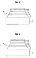
- a GaN semiconductor layer 20 having a multilayer structure and a first electrode 30 are formed over a sapphire substrate 10.
- the semiconductor layer 20 is grown, using, for example, a general semiconductor growing method.
- various methods for example, PVD such as sputtering, MOCVD using organic metal pre-cursor, and ion implanting, may be selectively used in accordance with the convenience of the process.
- the semiconductor layer 20 includes an n type semiconductor layer 21, an active layer 22, and a p type semiconductor layer 23. As shown in FIG. 3, the semiconductor layer 20 has a structure having an area which gradually reduces with distance from the substrate 10.
- a current diffusion layer 24 may be formed over the p type semiconductor layer 23, as shown in FIG. 4.
- an In x Ga 1-x N layer or an In x Ga 1-x N/GaN superlattice layer may be used.
- the current diffusion layer 24 can function to enhance mobility of carriers, and thus to cause current to flow smoothly.
- a current diffusion layer is also called a current transport enhanced layer (CTEL).
- CTL current transport enhanced layer
- the first electrode 30 is an ohmic electrode. Such an ohmic electrode is, in this embodiment, formed using a transparent electrode structure.
- the first electrode 30 is a p type electrode in this embodiment because it is formed over the p type semiconductor layer 23.
- a transparent electrode is used for the first electrode 30, as described above, it may, in a modification, be more advantageous to form the transparent electrode over the current diffusion layer 24, using a transparent conductive oxide (TCO).
- TCO transparent conductive oxide
- the work function of the current diffusion layer 24 may, as in this embodiment, be smaller than the work function of the p type GaN semiconductor layer as the p type semiconductor layer 23, but may, as in this embodiment be larger than the work function of the transparent electrode.
- the work function ranges of the current diffusion layer 24 and p type semiconductor layer 23 may, as in this embodiment, partially overlap with each other. Also, the work function ranges of the p type semiconductor layer 23 and transparent electrode may, as in this embodiment, partially overlap with each other.
- indium tin oxide ITO
- ITO indium tin oxide
- Other materials such as indium zinc oxide (IZO), aluminum zinc oxide (AZO), magnesium zinc oxide (MZO), or gallium zinc oxide (GZO), may also be used.
- a reflection electrode 40 is formed over the first electrode 30. It is preferred that the reflection electrode 40 be made of silver (Ag) or aluminum (Al). However other suitable materials known to the skilled person may be employed.
- a support layer is also be provided in this embodiment to support the semiconductor layer 20 in a process for separating the substrate 10 from the semiconductor layer 20, as will be described later.
- the support layer is made of metal or semiconductor containing Si.
- the first electrode 30 functions as a p type electrode.
- the sapphire substrate 10 is completely removed from the light emitting device chip, using a laser lift off (LLO) method.
- LLO laser lift off
- the separation of the substrate 10 may be achieved using methods other than the LLO method, for example, etching.
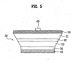
- a TCO layer 50 is formed over the structure obtained after the removal of the substrate 10 in an inverted state of the structure, as shown in FIG. 5.
- a second electrode 60 is formed, in the form of a metal pad, on the TCO layer 50.
- the TCO layer 50 functions to efficiently supply current to the semiconductor layer 20.
- an enhancement in light emission efficiency, an increase in light emission area, and a decrease in operating voltage can be achieved.
- the second electrode 60 can be formed in the form of, for example, a metal pad, to have a reduced area. Accordingly, the second electrode 60 does not reduce the light emission area.
- the semiconductor layer 20 may have a structure having an area gradually increasing as it extends from the first electrode 30 to the TCO layer 50. In accordance with this structure, it is possible to increase the light escape angle.
- the TCO layer 50 is made of ZnO. Also, AlZnO or InZnO produced by adding Al or In, as a dopant, to ZnO may be used.
- the effect of the TCO layer 50 may be small in this case because the ohmic contact between the TCO layer 50 and the n type semiconductor layer 21 of the semiconductor layer 20 may be insufficiently formed.
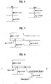
- FIG. 6 illustrates band structures of ITO and n type GaN semiconductor before the bonding thereof.
- ITO has a work function of about 4.7 eV and a band gap Bg of about 3.7 eV
- GaN has a band gap of about 3.44 eV.
- the Fermi level of ITO is equalized with a conduction band, namely, the Fermi level of n type GaN, as in a conductive metal, as shown in FIG. 7.
- a barrier ⁇ E c blocking flow of electrons and having a level of 1.7 eV is formed.
- the band structure is bent at the bonding surface, so that a barrier is formed in the conduction band at the bonding surface.
- ZnO has a work function of 4.2 eV and a band gap Bg of 3.37 eV.
- the Fermi level of ZnO is equalized with a conduction band, namely, the Fermi level of n type GaN, as in a conductive metal, as shown in FIG. 10.
- a barrier ⁇ E c blocking flow of electrons and having a level of 1.2 eV is formed.
- the case using ZnO and the case using AlZnO or InZnO added with a dopant are more advantageous in terms of flow of current.
- the TCO layer 50 which is made of a ZnO-based material as described above, can greatly improve the light escape angle, through which light escapes from the inside of the GaN material.
- the light escape angle through which light can directly escape from GaN having a refractive index of 2.35 to the external of the GaN (air), is about 25°.
- the light escape angle is greatly increased because "sin -1 (2.07/2.35)" is 61.74°.
- a GaN-based semiconductor layer 200 and a first electrode 300 are formed over a sapphire substrate 100.
- the semiconductor layer 200 includes an n type semiconductor layer 210, an active layer 220, and a p type semiconductor layer 230.
- the first electrode 300 may include a reflection electrode 400.
- a support layer, which is made of metal or semiconductor containing Si, may also be formed over the first electrode 300.
- the first electrode 300 functions as a p type electrode.
- the sapphire substrate 100 is completely removed from the light emitting device chip, using a laser lift off (LLO) method.
- LLO laser lift off
- a getter metal layer 500 is then deposited over the surface of the n type semiconductor layer 210, from which the substrate 100 has been removed, using a metal having nitrogen gettering characteristics, for example, Ti, Zr, or Cr.
- the getter metal layer 500 can exhibit a high reactivity to nitrogen (N) which is a Group V material in a semiconductor material of Group III to Group V such as GaN.
- the deposition of the getter metal such as Ti, Zr, or Cr is achieved by coating or doping the getter metal on or in an interface of the n type semiconductor layer 210 in a small amount.
- various methods for example, PVD such as sputtering, MOCVD using organic metal pre-cursor, and ion implanting, may be selectively used in accordance with the convenience of the process.
- a transparent conductive oxide (TCO) layer 600 having an appropriate refractive index is formed over the getter metal layer 500, in order to obtain a maximum light escape effect.
- TCO transparent conductive oxide
- the TCO layer 600 be made of indium tin oxide (ITO).
- TCO such as ITO may not form an effective ohmic contact with any of n type GaN and p type GaN, as shown in FIG. 15.
- the TCO layer 600 which is efficient in terms of refractive index, can be applied to a top layer in a light emitting device having a vertical structure, as in the above-described structure, considerable advantages in terms of light escape may be provided.
- Ga-N decomposition is observed at an ITO/GaN interface in a heat treatment.
- the ohmic contact of n type GaN generally reacts with nitrogen in a Ga-N surface, thereby causing the surface to be nitrogen deficient, and thus forming ohmic contact.
- the nitrogen getter metal layer 500 can achieve improvements in ohmic characteristics and device stability by removing nitrogen in the Ga-N structure.
- metal such as Ti can effectively prevent a degradation in electrode characteristics caused by formation of a compound because Ti easily forms a Ti-N compound, and the Ti-N exhibits conductivity as in metal.
- a second electrode 700 is formed, as an n type electrode, over the TCO layer 600.
- a chip structure is completely fabricated.
- the light escape angle through which light can directly escape from GaN having a refractive index of 2.35 to the external of the GaN (air), is about 25°.
- the light escape angle is greatly increased to 54.78°.
Landscapes
- Led Devices (AREA)
Abstract
Description
- The present invention relates to a light emitting device having a vertical structure. It more particularly relates to a light emitting device having a vertical structure which is capable of achieving an enhancement in light escape efficiency, and a method for manufacturing the same.
- Light emitting diodes (LEDs) are well known as a semiconductor light emitting device which converts current to light, to emit light. Since a red LED using GaAsP compound semiconductor became commercially available in 1962, it has been used, together with a GaP:N-based green LED, as a light source in electronic apparatuses, for image display.
- The wavelength of light emitted from such an LED depends on the semiconductor material used to fabricate the LED. This is because the wavelength of the emitted light depends on the band gap of the semiconductor material representing energy difference between valence-band electrons and conduction-band electrons.
- Gallium nitride (GaN) compound semiconductor has been highlighted. One of the reasons why GaN compound semiconductor has been highlighted is that it is possible to fabricate a semiconductor layer capable of emitting green, blue, or white light, using GaN in combination with other elements, for example, indium (In), aluminum (Al), etc.
- Thus, it is possible to adjust the wavelength of light to be emitted, using GaN in combination with other appropriate elements. Accordingly, where GaN is used, it is possible to appropriately determine the materials of a desired LED in accordance with the characteristics of the apparatus to which the LED is applied. For example, it is possible to fabricate a blue LED useful for optical recording or a white LED to replace a glow lamp.
- On the other hand, initially-developed green LEDs were fabricated using GaP. Since GaP is an indirect transition material causing a degradation in efficiency, the green LEDs fabricated using this material cannot practically produce light of pure green. By virtue of the recent success of growth of an InGaN thin film, however, it has been possible to fabricate a high-luminescent green LED.
- By virtue of the above-mentioned advantages and other advantages of GaN-based LEDs, the GaN-based LED market has rapidly grown. Also, techniques associated with GaN-based electro-optic devices have rapidly developed since the GaN-based LEDs became commercially available in 1994.
- GaN-based LEDs have been developed to exhibit light emission efficiency superior over that of glow lamps. Currently, the efficiency of GaN-based LEDs is substantially equal to that of fluorescent lamps. Thus, it is expected that the GaN-based LED market will grow significantly.
- Despite the rapid advancement in technologies of GaN-based semiconductor devices, the fabrication of GaN-based devices suffers from a great disadvantage of high-production costs. This disadvantage is closely related to difficulties associated with growing of a GaN thin film (epitaxial layer) and subsequent cutting of finished GaN-based devices.
- Such a GaN-based device is generally fabricated on a sapphire (Al2O3) substrate. This is because a sapphire wafer is commercially available in a size suited for the mass production of GaN-based devices, supports GaN epitaxial growth with a relatively high quality, and exhibits a high processability in a wide range of temperatures.
- Further, sapphire is chemically and thermally stable, and has a high-melting point enabling implementation of a high-temperature manufacturing process. Also, sapphire has a high bonding energy (122.4 Kcal/mole) and a high dielectric constant. In terms of a chemical structure, the sapphire is a crystalline aluminum oxide (Al2O3).
- Meanwhile, since sapphire is an insulating material, available LED devices manufactured using a sapphire substrate (or other insulating substrates) are practically limited to a lateral or vertical structure.
- In the lateral structure, all metal contacts for use in injection of electric current into LEDs are positioned on the top surface of the device structure (or on the same substrate surface). On the other hand, in the vertical structure, one metal contact is positioned on the top surface, and the other contact is positioned on the bottom surface of the device structure after removal of the sapphire (insulating) substrate.
- In addition, a flip chip bonding method has also been widely employed. In accordance with the flip chip bonding method, an LED chip, which has been separately prepared, is attached to a sub-mount of, for example, a silicon wafer or ceramic substrate having an excellent thermal conductivity, under the condition in which the LED chip is inverted.
- However, the lateral structure or the flip chip method suffers from problems associated with poor heat dissipation efficiency because the sapphire substrate has a thermal conductivity of about 27 W/mK, thus leading to a very high thermal resistance. Furthermore, the flip chip method has also disadvantages of requiring large numbers of photolithography process steps, thus resulting in complicated manufacturing processes.
- To this end, LED devices having a vertical structure have been highlighted in that the vertical structure involves removal of the sapphire substrate.
- In the fabrication of such a vertical LED structure, a laser lift off (LLO) method is used to remove the sapphire substrate, and thus to solve the problems caused by the sapphire substrate.
- That is, as shown in FIG. 1, over a sapphire substrate 1, a GaN thin film including an n
type GaN layer 2, anactive layer 3, and a ptype GaN layer 4 is formed. Ap type electrode 5 is formed over the GaN thin film. - An LLO method is applied to the chip as fabricated in the above-mentioned manner, to completely remove the sapphire substrate 1.
- In the LLO method, stress is applied to the GaN thin film upon incidence of a laser beam. In order to separate the sapphire substrate 1 and GaN thin film from each other, it is necessary to use a laser beam having a high energy density. The laser beam decomposes GaN into a metal element, namely, Ga, and nitrogen gas (N2).
- After removal of the substrate 1 as mentioned above, an n type electrode 7 is formed on the exposed n
type GaN layer 2, as shown in FIG. 2, to fabricate a chip structure. - In such a vertical LED structure, the n
type GaN layer 2 is arranged at the uppermost portion of the chip structure, as shown in the drawing. For this reason, the area of a contact region of the ntype GaN layer 2 considerably affects the total light emission efficiency. - Although it is advantageous, in terms of light escape, to reduce the area of the contact region, there may be a problem such as an increase in operating voltage because the reduced contact region causes an increase in the total resistance of the device or insufficient current spreading.
- Since the GaN material has a refractive index of 2.35, the angle, through which light from the LED is externally emitted without being fully reflected within the LED, is limited to 25° from a vertical line in the case in which the GaN material is directly in contact with air having a refractive index of 1.
- The present invention seeks to provide an improved light emitting device and a method for manufacturing the same.
- Embodiments of the present invention can provide a light emitting device having a vertical structure which is capable of achieving enhancements in light emission efficiency and light escape efficiency, using a transparent conductive oxide (TCO) laminated over a GaN semiconductor layer, and a getter metal forming ohmic contact between the GaN semiconductor layer and the TCO, and a method for manufacturing the same.
- Additional advantages and features of the invention will be set forth in part in the description which follows and in part will become apparent to those having ordinary skill in the art upon examination of the following or may be learned from practice of the invention. The objectives and other advantages of the invention may be realized and attained by the structure particularly pointed out in the written description and claims hereof as well as the drawings.
- In accordance with a first aspect of the invention, a light emitting device having a vertical structure comprises: a semiconductor layer having a first surface and a second surface; a first electrode arranged on the first surface of the semiconductor layer; a transparent conductive oxide (TCO) layer arranged on the second surface of the semiconductor layer; and a second electrode arranged on the TCO layer.
- In another aspect of the invention, a light emitting device having a vertical structure comprises: a first electrode; a semiconductor layer arranged on the first electrode; a metal layer having a reactivity to at least one of elements forming the semiconductor layer; a transparent conductive oxide (TCO) layer arranged on the metal layer; and a second electrode arranged on the TCO layer.
- In another aspect of the invention, a method for manufacturing a light emitting device having a vertical structure comprises: forming a semiconductor layer having a multilayer structure over a substrate; forming a first electrode on the semiconductor layer; forming a support layer made of metal or semiconductor over the first electrode; separating the substrate from the semiconductor layer; forming a transparent conductive oxide (TCO) layer over a substrate-separated surface of the semiconductor layer; and forming a second electrode on the TCO layer.
- It is to be understood that both the foregoing general description and the following detailed description of the present invention are exemplary and explanatory and are intended to provide further explanation of the invention as claimed.
- Embodiments of the invention will now be described by way of non-limiting example only, with reference to the drawings, in which:
- FIG. 1 is sectional view illustrating an example of a conventional process for manufacturing a light emitting device having a vertical structure;
- FIG. 2 is sectional view illustrating an example of a conventional light emitting device having a vertical structure;
- FIGs. 3 to 11 are sectional view illustrating a first embodiment of the invention, in which:
- FIG. 3 is a sectional view illustrating an example of a manufacturing process according to the invention;
- FIG. 4 is a sectional view illustrating another example of the manufacturing process according to the invention;
- FIG. 5 is a sectional view illustrating an example of a light emitting device having a vertical structure manufactured in accordance with the invention;
- FIG. 6 is a schematic diagram illustrating band structures of ITO and n type GaN;
- FIG. 7 is a schematic diagram illustrating a band structure formed in a bonded state of ITO and n type GaN;
- FIG. 8 is a schematic diagram illustrating a band structure formed when an electric field is applied to a bonded structure of ITO and n type GaN;
- FIG. 9 is a schematic diagram illustrating band structures of ZnO and n type GaN;
- FIG. 10 is a schematic diagram illustrating a band structure formed in a bonded state of ZnO and n type GaN;
- FIG. 11 is a schematic diagram illustrating a band structure formed when an electric field is applied to a bonded structure of ZnO and n type GaN; and
- FIGs. 12 to 15 are sectional views illustrating a second embodiment of the invention, in which:
- FIG. 12 is a sectional view illustrating an example of a manufacturing process according to the invention;
- FIG. 13 is a sectional view illustrating an example of a light emitting device having a vertical structure manufactured in accordance with the invention;
- FIG. 14 is a schematic view illustrating a heat treatment process; and
- FIG. 15 is a schematic diagram illustrating band structures of ITO and GaN.
- The present invention may be embodied in many alternate forms and should not be construed as limited to the embodiments set forth herein. Accordingly, while the invention is susceptible to various modifications and alternative forms, specific embodiments thereof are shown by way of example in the drawings and will herein be described in detail. It should be understood, however, that there is no intent to limit the invention to the particular forms disclosed, but on the contrary, the invention is to cover all modifications, equivalents, and alternatives falling within the scope of the invention as defined by the claims.
- Like numbers refer to like elements throughout the description of the figures. In the drawings, the thickness of layers and regions are exaggerated for clarity.
- It will be understood that when an element such as a layer, region or substrate is referred to as being "on" another element, it can be directly on the other element or intervening elements may also be present. It will also be understood that if part of an element, such as a surface, is referred to as "inner," it is further from the outside of the device than other parts of the element.
- In addition, relative terms, such as "beneath" and "overlies", may be used herein to describe one layer's or region's relationship to another layer or region as illustrated in the figures.
- It will be understood that these terms are intended to encompass different orientations of the device in addition to the orientation depicted in the figures. Finally, the term "directly" means that there are no intervening elements. As used herein, the term "and/or" includes any and all combinations of one or more of the associated listed items.
- It will be understood that, although the terms first, second, etc. may be used herein to describe various elements, components, regions, layers and/or sections, these elements, components, regions, layers and/or sections should not be limited by these terms.
- These terms are only used to distinguish one region, layer or section from another region, layer or section. Thus, a first region, layer or section discussed below could be termed a second region, layer or section, and similarly, a second region, layer or section may be termed a first region, layer or section without departing from the teachings of the present invention.
- As shown in FIG. 3, in order to manufacture a light emitting device, a
GaN semiconductor layer 20 having a multilayer structure and afirst electrode 30 are formed over asapphire substrate 10. - The
semiconductor layer 20 is grown, using, for example, a general semiconductor growing method. For the semiconductor growing method, various methods, for example, PVD such as sputtering, MOCVD using organic metal pre-cursor, and ion implanting, may be selectively used in accordance with the convenience of the process. - The
semiconductor layer 20 includes an ntype semiconductor layer 21, anactive layer 22, and a ptype semiconductor layer 23. As shown in FIG. 3, thesemiconductor layer 20 has a structure having an area which gradually reduces with distance from thesubstrate 10. - If necessary, a
current diffusion layer 24 may be formed over the ptype semiconductor layer 23, as shown in FIG. 4. For thecurrent diffusion layer 24, an InxGa1-xN layer or an InxGa1-xN/GaN superlattice layer may be used. - The
current diffusion layer 24 can function to enhance mobility of carriers, and thus to cause current to flow smoothly. In this regard, such a current diffusion layer is also called a current transport enhanced layer (CTEL). - The
first electrode 30 is an ohmic electrode. Such an ohmic electrode is, in this embodiment, formed using a transparent electrode structure. Thefirst electrode 30 is a p type electrode in this embodiment because it is formed over the ptype semiconductor layer 23. - Where a transparent electrode is used for the
first electrode 30, as described above, it may, in a modification, be more advantageous to form the transparent electrode over thecurrent diffusion layer 24, using a transparent conductive oxide (TCO). - In this structure, the work function of the
current diffusion layer 24 may, as in this embodiment, be smaller than the work function of the p type GaN semiconductor layer as the ptype semiconductor layer 23, but may, as in this embodiment be larger than the work function of the transparent electrode. - The work function ranges of the
current diffusion layer 24 and ptype semiconductor layer 23 may, as in this embodiment, partially overlap with each other. Also, the work function ranges of the ptype semiconductor layer 23 and transparent electrode may, as in this embodiment, partially overlap with each other. - For the TCO of the transparent electrode, indium tin oxide (ITO) may be used. Other materials, such as indium zinc oxide (IZO), aluminum zinc oxide (AZO), magnesium zinc oxide (MZO), or gallium zinc oxide (GZO), may also be used.
- In order to achieve an enhancement in reflection efficiency, a
reflection electrode 40 is formed over thefirst electrode 30. It is preferred that thereflection electrode 40 be made of silver (Ag) or aluminum (Al). However other suitable materials known to the skilled person may be employed. - Meanwhile, a support layer is also be provided in this embodiment to support the
semiconductor layer 20 in a process for separating thesubstrate 10 from thesemiconductor layer 20, as will be described later. In this embodiment the support layer is made of metal or semiconductor containing Si. - Where the
semiconductor layer 20 has a structure laminated in the above-described order, thefirst electrode 30 functions as a p type electrode. - After formation of a light emitting device chip, which includes the
semiconductor layer 20,first electrode 30, andreflection electrode 40 formed as described above, thesapphire substrate 10 is completely removed from the light emitting device chip, using a laser lift off (LLO) method. - In such an LLO method, stress is applied to a GaN-based thin film upon incidence of a laser beam. In order to separate the
sapphire substrate 10 from the GaN thin film, namely thesemiconductor layer 20, it is necessary to use a laser beam having a high energy density. The laser beam decomposes GaN into a metal element, namely, Ga, and nitrogen gas (N2). - In a modification, the separation of the
substrate 10 may be achieved using methods other than the LLO method, for example, etching. - Thereafter, a
TCO layer 50 is formed over the structure obtained after the removal of thesubstrate 10 in an inverted state of the structure, as shown in FIG. 5. Asecond electrode 60 is formed, in the form of a metal pad, on theTCO layer 50. - The
TCO layer 50 functions to efficiently supply current to thesemiconductor layer 20. Thus, an enhancement in light emission efficiency, an increase in light emission area, and a decrease in operating voltage can be achieved. - That is, since the total resistance of the device does not increase in spite of a reduction in contact region, effective current spreading is achieved. Accordingly, it is possible to decrease the operating voltage.
- Thus, the
second electrode 60 can be formed in the form of, for example, a metal pad, to have a reduced area. Accordingly, thesecond electrode 60 does not reduce the light emission area. - Meanwhile, as shown in the drawings, the
semiconductor layer 20 may have a structure having an area gradually increasing as it extends from thefirst electrode 30 to theTCO layer 50. In accordance with this structure, it is possible to increase the light escape angle. - In this embodiment the
TCO layer 50 is made of ZnO. Also, AlZnO or InZnO produced by adding Al or In, as a dopant, to ZnO may be used. - Although ITO may be used for the
TCO layer 50, the effect of theTCO layer 50 may be small in this case because the ohmic contact between theTCO layer 50 and the ntype semiconductor layer 21 of thesemiconductor layer 20 may be insufficiently formed. - FIG. 6 illustrates band structures of ITO and n type GaN semiconductor before the bonding thereof. Referring to FIG. 6, ITO has a work function of about 4.7 eV and a band gap Bg of about 3.7 eV, whereas GaN has a band gap of about 3.44 eV.
- When ITO and n type GaN semiconductor, which have characteristics as described above, are bonded, the Fermi level of ITO is equalized with a conduction band, namely, the Fermi level of n type GaN, as in a conductive metal, as shown in FIG. 7. In this case, a barrier ΔEc blocking flow of electrons and having a level of 1.7 eV is formed.
- That is, the band structure is bent at the bonding surface, so that a barrier is formed in the conduction band at the bonding surface.
- When a voltage (bias) is applied to the band structure in this state, the barrier is maintained at 1.7 eV, but the band structure is further bent. Accordingly, a tunneling phenomenon occurs at the barrier, as shown in FIG. 8. As a result, current flows. In this case, when the applied voltage is higher, an increased amount of current flows because the bending degree increases.
- When ZnO and n type GaN are bonded, a similar phenomenon occurs. Here, ZnO has a work function of 4.2 eV and a band gap Bg of 3.37 eV.
- When ZnO and n type GaN semiconductor, which have characteristics as described above, are bonded, the Fermi level of ZnO is equalized with a conduction band, namely, the Fermi level of n type GaN, as in a conductive metal, as shown in FIG. 10. In this case, a barrier ΔEc blocking flow of electrons and having a level of 1.2 eV is formed.
- Since the amount of current flowing in accordance with a tunneling phenomenon is proportional to Exp [(ΔEc)3/2], it is possible to generate a sufficient flow of current with a lower voltage, in the case in which ZnO and n type GaN are bonded.
- That is, as can be seen from the above description, the case using ZnO and the case using AlZnO or InZnO added with a dopant are more advantageous in terms of flow of current.
- The
TCO layer 50, which is made of a ZnO-based material as described above, can greatly improve the light escape angle, through which light escapes from the inside of the GaN material. - In accordance with a simple calculation, the light escape angle, through which light can directly escape from GaN having a refractive index of 2.35 to the external of the GaN (air), is about 25°. However, when a ZnO-based material is used for the
TCO layer 50, the light escape angle is greatly increased because "sin-1(2.07/2.35)" is 61.74°. - Hereinafter, a second embodiment of the present invention will be described with reference to FIGs. 12 to 15. In the following description, no explanation will be given of the same process as that of the first embodiment.
- As shown in FIG. 12, in order to manufacture a light emitting device according to this embodiment, a GaN-based
semiconductor layer 200 and afirst electrode 300 are formed over asapphire substrate 100. - As shown in FIG. 12, the
semiconductor layer 200 includes an ntype semiconductor layer 210, anactive layer 220, and a ptype semiconductor layer 230. In order to achieve an enhancement in reflection efficiency, thefirst electrode 300 may include areflection electrode 400. A support layer, which is made of metal or semiconductor containing Si, may also be formed over thefirst electrode 300. - Where the
semiconductor layer 200 has a structure laminated in the above-described order, thefirst electrode 300 functions as a p type electrode. - After formation of a light emitting device chip as described above, the
sapphire substrate 100 is completely removed from the light emitting device chip, using a laser lift off (LLO) method. - In such an LLO method, stress is applied to a GaN-based thin film upon incidence of a laser beam. In order to separate the
sapphire substrate 100 from the GaN thin film, it is necessary to use a laser beam having a high energy density. The laser beam decomposes GaN into a metal element, namely, Ga, and nitrogen gas (N2). - As shown in FIG. 13, a
getter metal layer 500 is then deposited over the surface of the ntype semiconductor layer 210, from which thesubstrate 100 has been removed, using a metal having nitrogen gettering characteristics, for example, Ti, Zr, or Cr. Thegetter metal layer 500 can exhibit a high reactivity to nitrogen (N) which is a Group V material in a semiconductor material of Group III to Group V such as GaN. - The deposition of the getter metal such as Ti, Zr, or Cr is achieved by coating or doping the getter metal on or in an interface of the n
type semiconductor layer 210 in a small amount. For the deposition method, various methods, for example, PVD such as sputtering, MOCVD using organic metal pre-cursor, and ion implanting, may be selectively used in accordance with the convenience of the process. - After the deposition of the
getter metal layer 500, a transparent conductive oxide (TCO)layer 600 having an appropriate refractive index is formed over thegetter metal layer 500, in order to obtain a maximum light escape effect. - It is preferred that the
TCO layer 600 be made of indium tin oxide (ITO). - After the formation of the
getter metal layer 500 andTCO layer 600 over thesemiconductor layer 200, a heat treatment is carried out, as shown in FIG. 14. - As is generally known, TCO such as ITO may not form an effective ohmic contact with any of n type GaN and p type GaN, as shown in FIG. 15.
- However, if the
TCO layer 600, which is efficient in terms of refractive index, can be applied to a top layer in a light emitting device having a vertical structure, as in the above-described structure, considerable advantages in terms of light escape may be provided. - As can be seen from the recent research results, Ga-N decomposition is observed at an ITO/GaN interface in a heat treatment. There is a report that the ohmic contact of n type GaN generally reacts with nitrogen in a Ga-N surface, thereby causing the surface to be nitrogen deficient, and thus forming ohmic contact.
- Accordingly, the nitrogen
getter metal layer 500 can achieve improvements in ohmic characteristics and device stability by removing nitrogen in the Ga-N structure. - As is well known, metal such as Ti can effectively prevent a degradation in electrode characteristics caused by formation of a compound because Ti easily forms a Ti-N compound, and the Ti-N exhibits conductivity as in metal.
- After the formation of
TCO layer 600 as described above, asecond electrode 700 is formed, as an n type electrode, over theTCO layer 600. Thus, a chip structure is completely fabricated. - Accordingly, it is possible to use ITO as the
TCO layer 600. As a result, it is possible to greatly improve the light escape angle, through which light escapes from the inside of the GaN material. - In accordance with a simple calculation, the light escape angle, through which light can directly escape from GaN having a refractive index of 2.35 to the external of the GaN (air), is about 25°. However, when ITO is used, the light escape angle is greatly increased to 54.78°.
- It will be apparent to those skilled in the art that various modifications and variations can be made in the present invention without departing from the scope thereof. Thus, it is intended that the present invention covers the modifications and variations of this invention provided they come within the scope of the claims including, but not limited to, the modifications and variations explicitly referred to above.
Claims (20)
- A light emitting device having a vertical structure, comprising:a semiconductor layer having a first surface and a second surface;a first electrode arranged on the first surface of the semiconductor layer;a transparent conductive oxide (TCO) layer arranged on the second surface of the semiconductor layer; anda second electrode arranged on the TCO layer.
- The light emitting device according to claim 1, wherein the semiconductor layer comprises:a p type semiconductor layer;an active layer arranged on the p type semiconductor layer; andan n type semiconductor layer arranged on the active layer.
- The light emitting device according to claim 1 or 2, further comprising:a current diffusion layer arranged between the semiconductor layer and the first electrode.
- The light emitting device according to claim 3, wherein the current diffusion layer comprises an InxGa1-xN layer or an InxGa1-xN/GaN superlattice layer.
- The light emitting device according to any preceding claim, wherein the first electrode comprises a reflection electrode.
- The light emitting device according to any preceding claim, further comprising:a support layer arranged on the first electrode, and made of metal or semiconductor containing Si.
- The light emitting device according to any preceding claim, wherein the semiconductor layer has an area gradually increasing as the semiconductor layer extends toward the TCO layer.
- The light emitting device according to any preceding claim, wherein the TCO layer is made of a conductive material having a refractive index higher than the refractive index of GaN.
- The light emitting device according to any preceding claim, wherein the TCO layer is made of one or more of indium tin oxide (ITO), ZnO, AlZnO, and InZnO.
- The light emitting device according to any preceding claim, further comprising:a getter metal layer arranged between the semiconductor layer and the TCO layer.
- The light emitting device according to claim 10, wherein the getter metal layer is made of at least one of Ti, Zr, and Cr.
- The light emitting device according to any preceding claim, wherein the semiconductor layer has inclined side surfaces.
- A light emitting device having a vertical structure, comprising:a first electrode;a semiconductor layer arranged on the first electrode;a metal layer having a reactivity to at least one of elements forming the semiconductor layer;a transparent conductive oxide (TCO) layer arranged on the metal layer; anda second electrode arranged on the TCO layer.
- The light emitting device according to claim 13, wherein the first electrode comprises:a reflection electrode; andan ohmic electrode arranged between the reflection electrode and the semiconductor layer.
- The light emitting device according to claim 13 or 14, wherein the metal layer is made of at least one of Ti, Zr, and Cr.
- The light emitting device according to claim 13, 14 or 15, wherein the first electrode is formed on a support layer made of metal or semiconductor containing Si.
- A method for manufacturing a light emitting device having a vertical structure, comprising:forming a semiconductor layer having a multilayer structure over a substrate;forming a first electrode on the semiconductor layer;forming a support layer made of metal or semiconductor over the first electrode;separating the substrate from the semiconductor layer;forming a transparent conductive oxide (TCO) layer over a substrate-separated surface of the semiconductor layer; andforming a second electrode on the TCO layer.
- The method according to claim 17, wherein the step of a TCO layer comprises forming the TCO layer over a getter metal layer.
- The method according to claim 18, further comprising:heat-treating the getter metal layer.
- The method according to claim 18 or 19, wherein the getter metal layer is formed using one of a sputtering method, an MOCVD method, and an ion implanting method.
Applications Claiming Priority (2)
| Application Number | Priority Date | Filing Date | Title |
|---|---|---|---|
| KR1020060015038A KR101113875B1 (en) | 2006-02-16 | 2006-02-16 | LED having vertical structure and the method of manufacturing the same |
| KR20060015037A KR101198764B1 (en) | 2006-02-16 | 2006-02-16 | LED having vertical structure and the method of manufacturing the same |
Publications (3)
| Publication Number | Publication Date |
|---|---|
| EP1821347A2 true EP1821347A2 (en) | 2007-08-22 |
| EP1821347A3 EP1821347A3 (en) | 2010-05-19 |
| EP1821347B1 EP1821347B1 (en) | 2018-01-03 |
Family
ID=37907565
Family Applications (1)
| Application Number | Title | Priority Date | Filing Date |
|---|---|---|---|
| EP07250583.7A Active EP1821347B1 (en) | 2006-02-16 | 2007-02-13 | Light emitting device having vertical structure and method for manufacturing the same |
Country Status (5)
| Country | Link |
|---|---|
| US (2) | US7700966B2 (en) |
| EP (1) | EP1821347B1 (en) |
| JP (2) | JP2007221146A (en) |
| CN (1) | CN102751415B (en) |
| TW (1) | TWI420699B (en) |
Cited By (2)
| Publication number | Priority date | Publication date | Assignee | Title |
|---|---|---|---|---|
| EP3462489A1 (en) * | 2017-09-29 | 2019-04-03 | Facebook Technologies, LLC | Mesa shaped micro light emitting diode with bottom n-contact |
| US10418510B1 (en) | 2017-12-22 | 2019-09-17 | Facebook Technologies, Llc | Mesa shaped micro light emitting diode with electroless plated N-contact |
Families Citing this family (6)
| Publication number | Priority date | Publication date | Assignee | Title |
|---|---|---|---|---|
| EP1821347B1 (en) * | 2006-02-16 | 2018-01-03 | LG Electronics Inc. | Light emitting device having vertical structure and method for manufacturing the same |
| JP4290745B2 (en) * | 2007-03-16 | 2009-07-08 | 豊田合成株式会社 | Method for manufacturing group III-V semiconductor device |
| WO2009072365A1 (en) * | 2007-12-07 | 2009-06-11 | Idemitsu Kosan Co., Ltd. | Amorphous transparent conductive film for gallium nitride compound semiconductor light-emitting device |
| DE102009018603B9 (en) * | 2008-04-25 | 2021-01-14 | Samsung Electronics Co., Ltd. | Lighting device and manufacturing method thereof |
| CN103367561B (en) * | 2012-03-30 | 2016-08-17 | 清华大学 | The preparation method of light emitting diode |
| US10020422B1 (en) * | 2017-09-29 | 2018-07-10 | Oculus Vr, Llc | Mesa shaped micro light emitting diode with bottom N-contact |
Family Cites Families (37)
| Publication number | Priority date | Publication date | Assignee | Title |
|---|---|---|---|---|
| JPH08167735A (en) * | 1994-12-12 | 1996-06-25 | Hitachi Cable Ltd | Light emitting element |
| US5917202A (en) * | 1995-12-21 | 1999-06-29 | Hewlett-Packard Company | Highly reflective contacts for light emitting semiconductor devices |
| US6229160B1 (en) * | 1997-06-03 | 2001-05-08 | Lumileds Lighting, U.S., Llc | Light extraction from a semiconductor light-emitting device via chip shaping |
| US6784463B2 (en) * | 1997-06-03 | 2004-08-31 | Lumileds Lighting U.S., Llc | III-Phospide and III-Arsenide flip chip light-emitting devices |
| JP3518289B2 (en) * | 1997-11-05 | 2004-04-12 | 松下電器産業株式会社 | Gallium nitride based compound semiconductor light emitting device |
| JP3680558B2 (en) * | 1998-05-25 | 2005-08-10 | 日亜化学工業株式会社 | Nitride semiconductor device |
| JP4183299B2 (en) * | 1998-03-25 | 2008-11-19 | 株式会社東芝 | Gallium nitride compound semiconductor light emitting device |
| JP3609661B2 (en) * | 1999-08-19 | 2005-01-12 | 株式会社東芝 | Semiconductor light emitting device |
| JP2001111106A (en) * | 1999-10-07 | 2001-04-20 | Sharp Corp | Gallium nitride based compound semiconductor light emitting device and method of manufacturing the same |
| JP2001217456A (en) * | 2000-02-03 | 2001-08-10 | Sharp Corp | Gallium nitride based compound semiconductor light emitting device |
| US6693352B1 (en) * | 2000-06-05 | 2004-02-17 | Emitronix Inc. | Contact structure for group III-V semiconductor devices and method of producing the same |
| JP3814151B2 (en) * | 2001-01-31 | 2006-08-23 | 信越半導体株式会社 | Light emitting element |
| US6987613B2 (en) * | 2001-03-30 | 2006-01-17 | Lumileds Lighting U.S., Llc | Forming an optical element on the surface of a light emitting device for improved light extraction |
| TW541723B (en) * | 2001-04-27 | 2003-07-11 | Shinetsu Handotai Kk | Method for manufacturing light-emitting element |
| US7148520B2 (en) * | 2001-10-26 | 2006-12-12 | Lg Electronics Inc. | Diode having vertical structure and method of manufacturing the same |
| JP4123830B2 (en) * | 2002-05-28 | 2008-07-23 | 松下電工株式会社 | LED chip |
| TW540170B (en) * | 2002-07-08 | 2003-07-01 | Arima Optoelectronics Corp | Ohmic contact structure of semiconductor light emitting device and its manufacturing method |
| TWI230473B (en) * | 2003-03-10 | 2005-04-01 | Sanken Electric Co Ltd | Semiconductor light emitting device and manufacturing method thereof |
| TWI240969B (en) * | 2003-06-06 | 2005-10-01 | Sanken Electric Co Ltd | Nitride semiconductor device and method for manufacturing same |
| KR100525545B1 (en) * | 2003-06-25 | 2005-10-31 | 엘지이노텍 주식회사 | Nitride semiconductor LED and fabrication method for thereof |
| JP2005039000A (en) * | 2003-07-18 | 2005-02-10 | Rohm Co Ltd | Semiconductor light emitting device and its manufacturing method |
| JP4766845B2 (en) * | 2003-07-25 | 2011-09-07 | シャープ株式会社 | Nitride-based compound semiconductor light-emitting device and method for manufacturing the same |
| JP2005051170A (en) * | 2003-07-31 | 2005-02-24 | Toyoda Gosei Co Ltd | Group iii nitride compound semiconductor light emitting element |
| JP3839799B2 (en) * | 2003-08-06 | 2006-11-01 | ローム株式会社 | Semiconductor light emitting device |
| JP2005064072A (en) * | 2003-08-20 | 2005-03-10 | Rohm Co Ltd | Semiconductor light emitting device |
| JP2005159310A (en) * | 2003-10-30 | 2005-06-16 | Matsushita Electric Ind Co Ltd | Semiconductor device and manufacturing method thereof |
| TWI234298B (en) * | 2003-11-18 | 2005-06-11 | Itswell Co Ltd | Semiconductor light emitting diode and method for manufacturing the same |
| JP2005217112A (en) * | 2004-01-29 | 2005-08-11 | Sumitomo Chemical Co Ltd | Nitride semiconductor light emitting device |
| JP4868709B2 (en) * | 2004-03-09 | 2012-02-01 | 三洋電機株式会社 | Light emitting element |
| TWI288486B (en) * | 2004-03-17 | 2007-10-11 | Epistar Corp | Light-emitting diode and method for manufacturing the same |
| JP2005268601A (en) * | 2004-03-19 | 2005-09-29 | Sumitomo Chemical Co Ltd | Compound semiconductor light emitting device |
| US7465592B2 (en) * | 2004-04-28 | 2008-12-16 | Verticle, Inc. | Method of making vertical structure semiconductor devices including forming hard and soft copper layers |
| TWM277111U (en) * | 2004-06-18 | 2005-10-01 | Super Nova Optoelectronics Cor | Vertical electrode structure for white-light LED |
| KR100730537B1 (en) * | 2004-06-25 | 2007-06-20 | 학교법인 성균관대학 | Light emitting diode with vertical structure and method manufacturing for the same |
| JP4740795B2 (en) * | 2005-05-24 | 2011-08-03 | エルジー エレクトロニクス インコーポレイティド | Rod type light emitting device and manufacturing method thereof |
| EP1821347B1 (en) * | 2006-02-16 | 2018-01-03 | LG Electronics Inc. | Light emitting device having vertical structure and method for manufacturing the same |
| CN101308887B (en) * | 2007-05-18 | 2010-09-29 | 富士迈半导体精密工业(上海)有限公司 | High-brightness light-emitting diode and its manufacturing method |
-
2007
- 2007-02-13 EP EP07250583.7A patent/EP1821347B1/en active Active
- 2007-02-15 TW TW096105707A patent/TWI420699B/en not_active IP Right Cessation
- 2007-02-16 US US11/706,977 patent/US7700966B2/en active Active
- 2007-02-16 JP JP2007036624A patent/JP2007221146A/en active Pending
- 2007-02-16 CN CN201210188762.XA patent/CN102751415B/en active Active
-
2010
- 2010-03-05 US US12/718,937 patent/US7868348B2/en active Active
-
2012
- 2012-11-05 JP JP2012243706A patent/JP2013034010A/en active Pending
Non-Patent Citations (1)
| Title |
|---|
| None |
Cited By (2)
| Publication number | Priority date | Publication date | Assignee | Title |
|---|---|---|---|---|
| EP3462489A1 (en) * | 2017-09-29 | 2019-04-03 | Facebook Technologies, LLC | Mesa shaped micro light emitting diode with bottom n-contact |
| US10418510B1 (en) | 2017-12-22 | 2019-09-17 | Facebook Technologies, Llc | Mesa shaped micro light emitting diode with electroless plated N-contact |
Also Published As
| Publication number | Publication date |
|---|---|
| US7700966B2 (en) | 2010-04-20 |
| TW200735424A (en) | 2007-09-16 |
| CN102751415B (en) | 2016-09-07 |
| EP1821347B1 (en) | 2018-01-03 |
| US20070252165A1 (en) | 2007-11-01 |
| JP2007221146A (en) | 2007-08-30 |
| EP1821347A3 (en) | 2010-05-19 |
| US20100155765A1 (en) | 2010-06-24 |
| TWI420699B (en) | 2013-12-21 |
| US7868348B2 (en) | 2011-01-11 |
| CN102751415A (en) | 2012-10-24 |
| JP2013034010A (en) | 2013-02-14 |
Similar Documents
| Publication | Publication Date | Title |
|---|---|---|
| US7687811B2 (en) | Vertical light emitting device having a photonic crystal structure | |
| US20070018183A1 (en) | Roughened high refractive index layer/LED for high light extraction | |
| US7868348B2 (en) | Light emitting device having vertical structure and method for manufacturing the same | |
| KR20090032207A (en) | Gallium nitride based light emitting diode device | |
| JP2014179654A (en) | GaN-BASED COMPOUND SEMICONDUCTOR LIGHT EMITTING ELEMENT, AND METHOD OF MANUFACTURING THE SAME | |
| CN103311391B (en) | LED crystal particle and preparation method thereof | |
| US8482034B2 (en) | Light emitting device | |
| KR101064068B1 (en) | Manufacturing method of light emitting device | |
| CN110021689A (en) | Light emitting diode and its manufacturing method | |
| CN101026215B (en) | Light emitting device with vertical structure and manufacturing method thereof | |
| KR101499954B1 (en) | fabrication of vertical structured light emitting diodes using group 3 nitride-based semiconductors and its related methods | |
| CN210040239U (en) | Light emitting diode | |
| US20060234411A1 (en) | Method of manufacturing nitride semiconductor light emitting diode | |
| KR20130020525A (en) | Semiconductor light emitting device and method manufacturing thereof | |
| KR20120066257A (en) | Semiconductor light emitting device | |
| KR20090112854A (en) | Group 3 nitride-based semiconductor light emitting diodes and methods to fabricate them | |
| TWI887590B (en) | Light-emitting device | |
| KR100918830B1 (en) | Vertical structure gallium nitride-based light emitting diode device and manufacturing method thereof | |
| CN110034219A (en) | Light emitting diode and its manufacturing method | |
| KR101113875B1 (en) | LED having vertical structure and the method of manufacturing the same | |
| KR20090032212A (en) | Nitride-based semiconductor light emitting device for flip chip | |
| KR101115571B1 (en) | GaN compound semiconductor light emitting element | |
| KR100635159B1 (en) | Nitride-based semiconductor light emitting device and its manufacturing method | |
| JP2011086855A (en) | Method of manufacturing semiconductor light-emitting element |
Legal Events
| Date | Code | Title | Description |
|---|---|---|---|
| PUAI | Public reference made under article 153(3) epc to a published international application that has entered the european phase |
Free format text: ORIGINAL CODE: 0009012 |
|
| AK | Designated contracting states |
Kind code of ref document: A2 Designated state(s): AT BE BG CH CY CZ DE DK EE ES FI FR GB GR HU IE IS IT LI LT LU LV MC NL PL PT RO SE SI SK TR |
|
| AX | Request for extension of the european patent |
Extension state: AL BA HR MK YU |
|
| PUAL | Search report despatched |
Free format text: ORIGINAL CODE: 0009013 |
|
| AK | Designated contracting states |
Kind code of ref document: A3 Designated state(s): AT BE BG CH CY CZ DE DK EE ES FI FR GB GR HU IE IS IT LI LT LU LV MC NL PL PT RO SE SI SK TR |
|
| AX | Request for extension of the european patent |
Extension state: AL BA HR MK RS |
|
| 17P | Request for examination filed |
Effective date: 20100719 |
|
| AKX | Designation fees paid |
Designated state(s): DE FI FR GB NL |
|
| RAP1 | Party data changed (applicant data changed or rights of an application transferred) |
Owner name: LG INNOTEK CO., LTD. Owner name: LG ELECTRONICS INC. |
|
| REG | Reference to a national code |
Ref country code: DE Ref legal event code: R079 Ref document number: 602007053604 Country of ref document: DE Free format text: PREVIOUS MAIN CLASS: H01L0033000000 Ipc: H01L0033420000 |
|
| GRAP | Despatch of communication of intention to grant a patent |
Free format text: ORIGINAL CODE: EPIDOSNIGR1 |
|
| RIC1 | Information provided on ipc code assigned before grant |
Ipc: H01L 33/42 20100101AFI20170628BHEP |
|
| INTG | Intention to grant announced |
Effective date: 20170727 |
|
| GRAS | Grant fee paid |
Free format text: ORIGINAL CODE: EPIDOSNIGR3 |
|
| GRAA | (expected) grant |
Free format text: ORIGINAL CODE: 0009210 |
|
| AK | Designated contracting states |
Kind code of ref document: B1 Designated state(s): DE FI FR GB NL |
|
| REG | Reference to a national code |
Ref country code: GB Ref legal event code: FG4D |
|
| REG | Reference to a national code |
Ref country code: DE Ref legal event code: R081 Ref document number: 602007053604 Country of ref document: DE Owner name: SUZHOU LEKIN SEMICONDUCTOR CO. LTD., TAICANG, CN Free format text: FORMER OWNERS: LG ELECTRONICS INC., SEOUL, KR; LG INNOTEK CO., LTD., SEOUL/SOUL, KR Ref country code: DE Ref legal event code: R081 Ref document number: 602007053604 Country of ref document: DE Owner name: LG ELECTRONICS INC., KR Free format text: FORMER OWNERS: LG ELECTRONICS INC., SEOUL, KR; LG INNOTEK CO., LTD., SEOUL/SOUL, KR |
|
| REG | Reference to a national code |
Ref country code: DE Ref legal event code: R096 Ref document number: 602007053604 Country of ref document: DE |
|
| REG | Reference to a national code |
Ref country code: NL Ref legal event code: MP Effective date: 20180103 |
|
| PG25 | Lapsed in a contracting state [announced via postgrant information from national office to epo] |
Ref country code: NL Free format text: LAPSE BECAUSE OF FAILURE TO SUBMIT A TRANSLATION OF THE DESCRIPTION OR TO PAY THE FEE WITHIN THE PRESCRIBED TIME-LIMIT Effective date: 20180103 |
|
| PG25 | Lapsed in a contracting state [announced via postgrant information from national office to epo] |
Ref country code: FI Free format text: LAPSE BECAUSE OF FAILURE TO SUBMIT A TRANSLATION OF THE DESCRIPTION OR TO PAY THE FEE WITHIN THE PRESCRIBED TIME-LIMIT Effective date: 20180103 |
|
| REG | Reference to a national code |
Ref country code: DE Ref legal event code: R097 Ref document number: 602007053604 Country of ref document: DE |
|
| PLBE | No opposition filed within time limit |
Free format text: ORIGINAL CODE: 0009261 |
|
| STAA | Information on the status of an ep patent application or granted ep patent |
Free format text: STATUS: NO OPPOSITION FILED WITHIN TIME LIMIT |
|
| REG | Reference to a national code |
Ref country code: FR Ref legal event code: ST Effective date: 20181031 |
|
| 26N | No opposition filed |
Effective date: 20181005 |
|
| GBPC | Gb: european patent ceased through non-payment of renewal fee |
Effective date: 20180403 |
|
| PG25 | Lapsed in a contracting state [announced via postgrant information from national office to epo] |
Ref country code: FR Free format text: LAPSE BECAUSE OF NON-PAYMENT OF DUE FEES Effective date: 20180305 Ref country code: GB Free format text: LAPSE BECAUSE OF NON-PAYMENT OF DUE FEES Effective date: 20180403 |
|
| REG | Reference to a national code |
Ref country code: DE Ref legal event code: R081 Ref document number: 602007053604 Country of ref document: DE Owner name: LG INNOTEK CO., LTD., KR Free format text: FORMER OWNERS: LG ELECTRONICS INC., SEOUL, KR; LG INNOTEK CO., LTD., SEOUL, KR Ref country code: DE Ref legal event code: R081 Ref document number: 602007053604 Country of ref document: DE Owner name: SUZHOU LEKIN SEMICONDUCTOR CO. LTD., TAICANG, CN Free format text: FORMER OWNERS: LG ELECTRONICS INC., SEOUL, KR; LG INNOTEK CO., LTD., SEOUL, KR Ref country code: DE Ref legal event code: R081 Ref document number: 602007053604 Country of ref document: DE Owner name: LG ELECTRONICS INC., KR Free format text: FORMER OWNERS: LG ELECTRONICS INC., SEOUL, KR; LG INNOTEK CO., LTD., SEOUL, KR |
|
| REG | Reference to a national code |
Ref country code: DE Ref legal event code: R081 Ref document number: 602007053604 Country of ref document: DE Owner name: LG INNOTEK CO., LTD., KR Free format text: FORMER OWNERS: LG ELECTRONICS INC., SEOUL, KR; SUZHOU LEKIN SEMICONDUCTOR CO. LTD., TAICANG, SUZHOU, CN Ref country code: DE Ref legal event code: R081 Ref document number: 602007053604 Country of ref document: DE Owner name: LG ELECTRONICS INC., KR Free format text: FORMER OWNERS: LG ELECTRONICS INC., SEOUL, KR; SUZHOU LEKIN SEMICONDUCTOR CO. LTD., TAICANG, SUZHOU, CN |
|
| REG | Reference to a national code |
Ref country code: DE Ref legal event code: R079 Ref document number: 602007053604 Country of ref document: DE Free format text: PREVIOUS MAIN CLASS: H01L0033420000 Ipc: H10H0020833000 |
|
| PGFP | Annual fee paid to national office [announced via postgrant information from national office to epo] |
Ref country code: DE Payment date: 20250120 Year of fee payment: 19 |