JP4183299B2 - Gallium nitride compound semiconductor light emitting device - Google Patents
Gallium nitride compound semiconductor light emitting device Download PDFInfo
- Publication number
- JP4183299B2 JP4183299B2 JP07747798A JP7747798A JP4183299B2 JP 4183299 B2 JP4183299 B2 JP 4183299B2 JP 07747798 A JP07747798 A JP 07747798A JP 7747798 A JP7747798 A JP 7747798A JP 4183299 B2 JP4183299 B2 JP 4183299B2
- Authority
- JP
- Japan
- Prior art keywords
- layer
- electrode
- metal layer
- light emitting
- emitting device
- Prior art date
- Legal status (The legal status is an assumption and is not a legal conclusion. Google has not performed a legal analysis and makes no representation as to the accuracy of the status listed.)
- Expired - Fee Related
Links
- 239000004065 semiconductor Substances 0.000 title claims description 63
- -1 Gallium nitride compound Chemical class 0.000 title claims description 17
- 229910002601 GaN Inorganic materials 0.000 title description 49
- 229910052751 metal Inorganic materials 0.000 claims description 76
- 239000002184 metal Substances 0.000 claims description 76
- KDLHZDBZIXYQEI-UHFFFAOYSA-N Palladium Chemical compound [Pd] KDLHZDBZIXYQEI-UHFFFAOYSA-N 0.000 claims description 62
- 239000010931 gold Substances 0.000 claims description 31
- 239000011777 magnesium Substances 0.000 claims description 27
- 229910052763 palladium Inorganic materials 0.000 claims description 22
- PCHJSUWPFVWCPO-UHFFFAOYSA-N gold Chemical compound [Au] PCHJSUWPFVWCPO-UHFFFAOYSA-N 0.000 claims description 16
- 229910052737 gold Inorganic materials 0.000 claims description 16
- FYYHWMGAXLPEAU-UHFFFAOYSA-N Magnesium Chemical compound [Mg] FYYHWMGAXLPEAU-UHFFFAOYSA-N 0.000 claims description 15
- 229910052749 magnesium Inorganic materials 0.000 claims description 15
- AMGQUBHHOARCQH-UHFFFAOYSA-N indium;oxotin Chemical compound [In].[Sn]=O AMGQUBHHOARCQH-UHFFFAOYSA-N 0.000 claims description 3
- 239000010936 titanium Substances 0.000 description 31
- 239000000463 material Substances 0.000 description 18
- RTAQQCXQSZGOHL-UHFFFAOYSA-N Titanium Chemical compound [Ti] RTAQQCXQSZGOHL-UHFFFAOYSA-N 0.000 description 16
- 229910052719 titanium Inorganic materials 0.000 description 16
- PXHVJJICTQNCMI-UHFFFAOYSA-N Nickel Chemical compound [Ni] PXHVJJICTQNCMI-UHFFFAOYSA-N 0.000 description 15
- 239000000758 substrate Substances 0.000 description 14
- 239000010409 thin film Substances 0.000 description 13
- JMASRVWKEDWRBT-UHFFFAOYSA-N Gallium nitride Chemical compound [Ga]#N JMASRVWKEDWRBT-UHFFFAOYSA-N 0.000 description 12
- 238000000034 method Methods 0.000 description 12
- 229910052594 sapphire Inorganic materials 0.000 description 11
- 239000010980 sapphire Substances 0.000 description 11
- 150000001875 compounds Chemical class 0.000 description 9
- BASFCYQUMIYNBI-UHFFFAOYSA-N platinum Chemical compound [Pt] BASFCYQUMIYNBI-UHFFFAOYSA-N 0.000 description 9
- 239000010949 copper Substances 0.000 description 8
- 239000010948 rhodium Substances 0.000 description 8
- WFKWXMTUELFFGS-UHFFFAOYSA-N tungsten Chemical compound [W] WFKWXMTUELFFGS-UHFFFAOYSA-N 0.000 description 8
- 229910052721 tungsten Inorganic materials 0.000 description 8
- 239000010937 tungsten Substances 0.000 description 8
- 238000000137 annealing Methods 0.000 description 7
- 239000010408 film Substances 0.000 description 7
- 229910052759 nickel Inorganic materials 0.000 description 6
- 238000000059 patterning Methods 0.000 description 5
- RYGMFSIKBFXOCR-UHFFFAOYSA-N Copper Chemical compound [Cu] RYGMFSIKBFXOCR-UHFFFAOYSA-N 0.000 description 4
- ZOKXTWBITQBERF-UHFFFAOYSA-N Molybdenum Chemical compound [Mo] ZOKXTWBITQBERF-UHFFFAOYSA-N 0.000 description 4
- 229910017052 cobalt Inorganic materials 0.000 description 4
- 239000010941 cobalt Substances 0.000 description 4
- GUTLYIVDDKVIGB-UHFFFAOYSA-N cobalt atom Chemical compound [Co] GUTLYIVDDKVIGB-UHFFFAOYSA-N 0.000 description 4
- 229910052802 copper Inorganic materials 0.000 description 4
- 229910052735 hafnium Inorganic materials 0.000 description 4
- VBJZVLUMGGDVMO-UHFFFAOYSA-N hafnium atom Chemical compound [Hf] VBJZVLUMGGDVMO-UHFFFAOYSA-N 0.000 description 4
- 229910052741 iridium Inorganic materials 0.000 description 4
- GKOZUEZYRPOHIO-UHFFFAOYSA-N iridium atom Chemical compound [Ir] GKOZUEZYRPOHIO-UHFFFAOYSA-N 0.000 description 4
- 238000010030 laminating Methods 0.000 description 4
- 238000004519 manufacturing process Methods 0.000 description 4
- 229910052750 molybdenum Inorganic materials 0.000 description 4
- 239000011733 molybdenum Substances 0.000 description 4
- 229910052703 rhodium Inorganic materials 0.000 description 4
- MHOVAHRLVXNVSD-UHFFFAOYSA-N rhodium atom Chemical compound [Rh] MHOVAHRLVXNVSD-UHFFFAOYSA-N 0.000 description 4
- 229910052706 scandium Inorganic materials 0.000 description 4
- SIXSYDAISGFNSX-UHFFFAOYSA-N scandium atom Chemical compound [Sc] SIXSYDAISGFNSX-UHFFFAOYSA-N 0.000 description 4
- VSZWPYCFIRKVQL-UHFFFAOYSA-N selanylidenegallium;selenium Chemical compound [Se].[Se]=[Ga].[Se]=[Ga] VSZWPYCFIRKVQL-UHFFFAOYSA-N 0.000 description 4
- 229910052715 tantalum Inorganic materials 0.000 description 4
- GUVRBAGPIYLISA-UHFFFAOYSA-N tantalum atom Chemical compound [Ta] GUVRBAGPIYLISA-UHFFFAOYSA-N 0.000 description 4
- LEONUFNNVUYDNQ-UHFFFAOYSA-N vanadium atom Chemical compound [V] LEONUFNNVUYDNQ-UHFFFAOYSA-N 0.000 description 4
- 239000000853 adhesive Substances 0.000 description 3
- 230000001070 adhesive effect Effects 0.000 description 3
- 230000000694 effects Effects 0.000 description 3
- 229910052697 platinum Inorganic materials 0.000 description 3
- 229910052782 aluminium Inorganic materials 0.000 description 2
- 230000007774 longterm Effects 0.000 description 2
- 238000001020 plasma etching Methods 0.000 description 2
- 229910001218 Gallium arsenide Inorganic materials 0.000 description 1
- BQCADISMDOOEFD-UHFFFAOYSA-N Silver Chemical compound [Ag] BQCADISMDOOEFD-UHFFFAOYSA-N 0.000 description 1
- 239000000956 alloy Substances 0.000 description 1
- 229910045601 alloy Inorganic materials 0.000 description 1
- XAGFODPZIPBFFR-UHFFFAOYSA-N aluminium Chemical compound [Al] XAGFODPZIPBFFR-UHFFFAOYSA-N 0.000 description 1
- 230000015572 biosynthetic process Effects 0.000 description 1
- 239000013078 crystal Substances 0.000 description 1
- 238000000151 deposition Methods 0.000 description 1
- 230000008021 deposition Effects 0.000 description 1
- 230000006866 deterioration Effects 0.000 description 1
- 239000007772 electrode material Substances 0.000 description 1
- 238000005530 etching Methods 0.000 description 1
- 238000002347 injection Methods 0.000 description 1
- 239000007924 injection Substances 0.000 description 1
- 150000002739 metals Chemical class 0.000 description 1
- 238000001552 radio frequency sputter deposition Methods 0.000 description 1
- 229910052709 silver Inorganic materials 0.000 description 1
- 239000004332 silver Substances 0.000 description 1
- 238000002230 thermal chemical vapour deposition Methods 0.000 description 1
- XOLBLPGZBRYERU-UHFFFAOYSA-N tin dioxide Chemical compound O=[Sn]=O XOLBLPGZBRYERU-UHFFFAOYSA-N 0.000 description 1
- 229910001887 tin oxide Inorganic materials 0.000 description 1
- 238000001771 vacuum deposition Methods 0.000 description 1
Images


Classifications
-
- H—ELECTRICITY
- H01—ELECTRIC ELEMENTS
- H01L—SEMICONDUCTOR DEVICES NOT COVERED BY CLASS H10
- H01L33/00—Semiconductor devices having potential barriers specially adapted for light emission; Processes or apparatus specially adapted for the manufacture or treatment thereof or of parts thereof; Details thereof
- H01L33/36—Semiconductor devices having potential barriers specially adapted for light emission; Processes or apparatus specially adapted for the manufacture or treatment thereof or of parts thereof; Details thereof characterised by the electrodes
- H01L33/40—Materials therefor
- H01L33/42—Transparent materials
-
- H—ELECTRICITY
- H01—ELECTRIC ELEMENTS
- H01L—SEMICONDUCTOR DEVICES NOT COVERED BY CLASS H10
- H01L2224/00—Indexing scheme for arrangements for connecting or disconnecting semiconductor or solid-state bodies and methods related thereto as covered by H01L24/00
- H01L2224/01—Means for bonding being attached to, or being formed on, the surface to be connected, e.g. chip-to-package, die-attach, "first-level" interconnects; Manufacturing methods related thereto
- H01L2224/10—Bump connectors; Manufacturing methods related thereto
- H01L2224/15—Structure, shape, material or disposition of the bump connectors after the connecting process
- H01L2224/16—Structure, shape, material or disposition of the bump connectors after the connecting process of an individual bump connector
- H01L2224/161—Disposition
- H01L2224/16151—Disposition the bump connector connecting between a semiconductor or solid-state body and an item not being a semiconductor or solid-state body, e.g. chip-to-substrate, chip-to-passive
- H01L2224/16221—Disposition the bump connector connecting between a semiconductor or solid-state body and an item not being a semiconductor or solid-state body, e.g. chip-to-substrate, chip-to-passive the body and the item being stacked
- H01L2224/16245—Disposition the bump connector connecting between a semiconductor or solid-state body and an item not being a semiconductor or solid-state body, e.g. chip-to-substrate, chip-to-passive the body and the item being stacked the item being metallic
-
- H—ELECTRICITY
- H01—ELECTRIC ELEMENTS
- H01L—SEMICONDUCTOR DEVICES NOT COVERED BY CLASS H10
- H01L2224/00—Indexing scheme for arrangements for connecting or disconnecting semiconductor or solid-state bodies and methods related thereto as covered by H01L24/00
- H01L2224/01—Means for bonding being attached to, or being formed on, the surface to be connected, e.g. chip-to-package, die-attach, "first-level" interconnects; Manufacturing methods related thereto
- H01L2224/42—Wire connectors; Manufacturing methods related thereto
- H01L2224/47—Structure, shape, material or disposition of the wire connectors after the connecting process
- H01L2224/48—Structure, shape, material or disposition of the wire connectors after the connecting process of an individual wire connector
- H01L2224/4805—Shape
- H01L2224/4809—Loop shape
- H01L2224/48091—Arched
-
- H—ELECTRICITY
- H01—ELECTRIC ELEMENTS
- H01L—SEMICONDUCTOR DEVICES NOT COVERED BY CLASS H10
- H01L2224/00—Indexing scheme for arrangements for connecting or disconnecting semiconductor or solid-state bodies and methods related thereto as covered by H01L24/00
- H01L2224/01—Means for bonding being attached to, or being formed on, the surface to be connected, e.g. chip-to-package, die-attach, "first-level" interconnects; Manufacturing methods related thereto
- H01L2224/42—Wire connectors; Manufacturing methods related thereto
- H01L2224/47—Structure, shape, material or disposition of the wire connectors after the connecting process
- H01L2224/48—Structure, shape, material or disposition of the wire connectors after the connecting process of an individual wire connector
- H01L2224/481—Disposition
- H01L2224/48151—Connecting between a semiconductor or solid-state body and an item not being a semiconductor or solid-state body, e.g. chip-to-substrate, chip-to-passive
- H01L2224/48221—Connecting between a semiconductor or solid-state body and an item not being a semiconductor or solid-state body, e.g. chip-to-substrate, chip-to-passive the body and the item being stacked
- H01L2224/48245—Connecting between a semiconductor or solid-state body and an item not being a semiconductor or solid-state body, e.g. chip-to-substrate, chip-to-passive the body and the item being stacked the item being metallic
- H01L2224/48247—Connecting between a semiconductor or solid-state body and an item not being a semiconductor or solid-state body, e.g. chip-to-substrate, chip-to-passive the body and the item being stacked the item being metallic connecting the wire to a bond pad of the item
-
- H—ELECTRICITY
- H01—ELECTRIC ELEMENTS
- H01L—SEMICONDUCTOR DEVICES NOT COVERED BY CLASS H10
- H01L2224/00—Indexing scheme for arrangements for connecting or disconnecting semiconductor or solid-state bodies and methods related thereto as covered by H01L24/00
- H01L2224/01—Means for bonding being attached to, or being formed on, the surface to be connected, e.g. chip-to-package, die-attach, "first-level" interconnects; Manufacturing methods related thereto
- H01L2224/42—Wire connectors; Manufacturing methods related thereto
- H01L2224/47—Structure, shape, material or disposition of the wire connectors after the connecting process
- H01L2224/48—Structure, shape, material or disposition of the wire connectors after the connecting process of an individual wire connector
- H01L2224/481—Disposition
- H01L2224/48151—Connecting between a semiconductor or solid-state body and an item not being a semiconductor or solid-state body, e.g. chip-to-substrate, chip-to-passive
- H01L2224/48221—Connecting between a semiconductor or solid-state body and an item not being a semiconductor or solid-state body, e.g. chip-to-substrate, chip-to-passive the body and the item being stacked
- H01L2224/48245—Connecting between a semiconductor or solid-state body and an item not being a semiconductor or solid-state body, e.g. chip-to-substrate, chip-to-passive the body and the item being stacked the item being metallic
- H01L2224/48257—Connecting between a semiconductor or solid-state body and an item not being a semiconductor or solid-state body, e.g. chip-to-substrate, chip-to-passive the body and the item being stacked the item being metallic connecting the wire to a die pad of the item
-
- H—ELECTRICITY
- H01—ELECTRIC ELEMENTS
- H01L—SEMICONDUCTOR DEVICES NOT COVERED BY CLASS H10
- H01L2224/00—Indexing scheme for arrangements for connecting or disconnecting semiconductor or solid-state bodies and methods related thereto as covered by H01L24/00
- H01L2224/01—Means for bonding being attached to, or being formed on, the surface to be connected, e.g. chip-to-package, die-attach, "first-level" interconnects; Manufacturing methods related thereto
- H01L2224/42—Wire connectors; Manufacturing methods related thereto
- H01L2224/47—Structure, shape, material or disposition of the wire connectors after the connecting process
- H01L2224/49—Structure, shape, material or disposition of the wire connectors after the connecting process of a plurality of wire connectors
- H01L2224/491—Disposition
- H01L2224/49105—Connecting at different heights
- H01L2224/49107—Connecting at different heights on the semiconductor or solid-state body
Landscapes
- Engineering & Computer Science (AREA)
- Manufacturing & Machinery (AREA)
- Computer Hardware Design (AREA)
- Microelectronics & Electronic Packaging (AREA)
- Power Engineering (AREA)
- Led Devices (AREA)
Description
【0001】
【発明の属する技術分野】
本発明は、窒化ガリウム系化合物半導体発光素子およびその製造方法に関する。より詳しくは、本発明は、基板上にGaN、InGaN、GaAlNなどの窒化ガリウム系化合物半導体層が積層された発光素子において、付着強度が高く、接触抵抗も低い電極を有する窒化ガリウム系化合物半導体発光素子およびその製造方法ならびに発光装置に関する。
【0002】
【従来の技術】
近年、Alx Gay In1-x-y N(O≦x≦1,O≦y≦1,x+y≦1)であらわされる窒化ガリウム系化合物半導体が紫外光領域から青色あるいは緑色発光ダイオード(LED)の材料として注目されている。このような材料の化合物半導体を使うことによって、これまで困難であった発光強度の高い紫外光、青色、緑色等の発光が可能となった。このような窒化ガリウム系化合物半導体は、一般に絶縁性基板であるサファイア基板上に成長されるため、GaAs系の発光素子のように基板の裏面に電極を設けることができない。このため結晶成長した半導体層側にアノード電極とカソード電極の両方を形成することが必要である。
【0003】
特に、窒化ガリウム系化合物半導体を用いた半導体素子の場合は、サファイア基板が発光波長に対して透光性を有するため、電極面を下側にしてマウントし、サファイア基板側から光を取り出す構造が一般的である。
【0004】
図7は、従来の窒化ガリウム系化合物半導体素子の構造例を表す概略図である。すなわち、発光素子は、サファイア基板1にGaNバッファ層2、n型GaN層3とp型GaN層4が結晶成長されて、p型GaN層4の一部がエッチング除去されてn型GaN層3が露出されており、p型GaN層4上にp側電極15、n型GaN層上にn側電極14が形成されている。このような発光素子は、リードフレーム17上に電極形成面を下側にして銀ペースト等の導電性接着材料16でマウントされている。
【0005】
【発明が解決しようとする課題】
図7に示したような従来の半導体発光素子では、p型GaN層4からn型GaN層2に電流が注入されて生じた発光が、p側電極15で反射されてサファイア基板1を通して外部に取り出される。しかし、このような従来の構造の窒化ガリウム系化合物半導体発光素子では、導電性接着材料16がリードフレーム17、17の間(図7の符号A)や、pn接合の間(図7の符号B)にまで広がり易く、電極間あるいは接合間でショートが生じやすい。その結果として、素子のマウントの際の歩留まりが著しく低下するばかりでなく、長期信頼性も劣化しやすいという問題があった。
【0006】
さらに、リードフレームと素子のマウント位置精度が高精度であることが必要とされるため量産性に欠けるという問題もある。これらの問題を避けるためには素子サイズを大きくしてリードフレーム17、17の間隔を広くすれば良いが、ウエハからとれるチップ数が減少しコストが高くなるという問題が生ずる。
【0007】
一方、発光素子の順方向電圧を低下させるためには、電極と窒化ガリウム半導体層とがオーミック接触をしている必要がある。従来は、n側電極としては、アルミニウム(Al)を含む電極、p側電極にはニッケル(Ni)や金(Au)を含む電極が用いられていた。ところが、これらの材料を用いた電極では必ずしも好ましいオーミック接触は得られていないばかりか、AlやNiはGaN層に侵入して信頼性の低下も招いていた。
【0008】
本発明は、このような事情に鑑みてなされたものである。すなわち、その目的は、電極の半導体層への密着性向上、オーミック特性の改善、薄膜金属と透明電極の組み含わせによる外部量子効率の改善を実現することができる窒化ガリウム系化合物半導体発光素子およびその製造方法を提供することにある。
【0009】
本発明の一態様によれば、窒化化合物半導体からなるn型半導体層と、
前記n型半導体層の上に形成されるn型電極と、
前記n型半導体層の上に、前記n型電極と分離して形成されるp型半導体層と、
前記p型半導体層の上に形成されるp型電極と、を備え、
前記n型電極は、
前記n型半導体層の上に形成されるパラジウム(Pd)からなる第1の金属層と、
前記第1の金属層の上に形成される金(Au)からなる第2の金属層と、を有し、
前記p型電極は、
前記p型半導体層の上に形成されるマグネシウム(Mg)からなる第3の金属層と、
前記第3の金属層の上に形成されるパラジウム(Pd)からなる第4の金属層と、
前記第4の金属層の上に形成されるITO( Indium Tin Oxide )からなる第5の金属層と、を有することを特徴とする窒化ガリウム系化合物半導体発光素子が提供される。
【0021】
本発明によれば、電極の密着性向上、オーミック特性の改善、薄膜金属と透明電極との組み合わせによる外部量子効率の改善がはかられた。また、電極面を下にしてマウントしサファイア基板側から光を取り出す構成ではないので、従来の問題点であった、電極間あるいは接合間でのショート、マウントの際の歩留まりの著しい低下、長期信頼性の劣化等々の問題点が解決される。さらに、カップ型のリードフレームを使うことができるため、効率良く光を取り出すことができる。
【0022】
【発明の実施の形態】
以下に図面を参照しつつ、本発明の実施の形態について説明する。
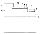
図1は、本発明の第1の実施の形態に係る窒化ガリウム系化合物半導体発光素子の構造を例示する概略断面図である。すなわち、本発明の発光素子は、サファイア基板1上に積層された窒化ガリウム系半導体層2〜4からなる積層構造を有する。また、素子のp側には、3層の金属層7〜9からなるp側電極と透明電極10とが積層され、電極パッド12に接続されている。また、n側においては、金属層5、6からなるn側電極が設けられている。
【0023】
ここで、p側電極を形成する3層の金属層7〜9のそれぞれの材料としては、以下に挙げるいずれかが用いられる。
すなわち、第1の金属層7は、電極とコンタクト層4との付着強度を維持し、オーミック接触を確保する役割を有する。その材料としては、チタン(Ti)、モリブデン(Mo)、タングステン(W)、マグネシウム(Mg)のうちのいずれかが用いられる。また、その層厚としては、5nm以下であることが望ましい。これよりも厚いと、接触抵抗が上昇し、電極の付着強度が低下する傾向がみられたからである。
また、第2の金属層8も、電極とコンタクト層4との付着強度を維持し、オーミック接触を確保する役割を有する。その材料としては、チタン(Ti)、ニッケル(Ni)、モリブデン(Mo)、タングステン(W)、マグネシウム(Mg)、金(Au)のうちのいずれかが用いられる。また、その層厚としては、5nm以下であることが望ましい。これよりも厚いと、接触抵抗が上昇し、電極の付着強度が低下する傾向がみられたからである。
また、第3の金属層9は、コンタクト層4とのオーミック接触を改善する役割を有する。その材料としては、パラジウム(Pd)、スカンジウム(Sc)、バナジュウム(V)、ジルコニウム(Zr)、ハフニウム(Hf)、タンタル(Ta)、ロジウム(Rh)、イリジウム(Ir)、コバルト(Co)、銅(Cu)、タングステン(W)、白金(Pt)のうちのいずれかが用いられる。また、その層厚としては、10nm以下であることが望ましい。これよりも厚いと、電極の付着強度が低下する傾向がみられたからである。
さらに、これらの薄膜金属層の上に透明電極層10を積層することにより、電極のシート抵抗を大幅に低減することができる。
【0024】
ここでは、p側電極の第1の金属層7としてチタン(Ti)、第2の金属層としてマグネシウム(Mg)をそれぞれ用いた場合を例示する。
【0025】
一方、n側電極の第1の金属層5は、オーミック接触を確保する役割を有する。その材料としては、パラジウム(Pd)、スカンジウム(Sc)、バナジウム(V)、ジルコニウム(Zr)、ハフニウム(Hf)、タンタル(Ta)、ロジウム(Rh)、イリジウム(Ir)、コバルト(Co)、銅(Cu)のうちのいずれかが用いられる。ここでは、第1の金属層5の材料としてパラジウム(Pd)を用いた場合について説明する。
【0026】
また、n側電極の第2の金属層6の材料としては、金(Au)が用いられる。本実施形態にかかる半導体発光素子の製造工程について概説すれば以下の如くである。
まず、サファイア基板1の上に、GaNバッファ層2、n型GaN層3、p型GaN層4を順次結晶成長させる。次に、p型GaN層4をPEP法によりパターニングし、RIE(reactive ion etching)法等によりエッチングしてn型GaN層3の一部を露出させる。
【0027】
次に、PEP法を用いてパターニングし、n側電極としてn型GaN層3の上にパラジウム(Pd)膜5、金(Au)膜6等を蒸着し、リフトオフによりパターニング形成する。
【0028】
次に、PEP法によりパターニング後、p型GaN層4の上に真空蒸着法により、厚さ1nmのチタン(Ti)層7、厚さ1nmのマグネシウム(Mg)層8、厚さ10nmのPd電極9を順次形成し、さらに、RFスパッタ法により酸化インジウム錫(indium tin oxide:lT0)膜10を形成後、リフトオフ法によってパターンを形成する。
【0029】
次に、p側薄膜電極と半導体層間の密着性、オーミック性を向上のため、またn側電極のオーミック性向上のため450℃、20秒程度のフラッシュアニールを行う。但し、半導体層表面に酸化物等がなく十分に清浄な状態であれば、このフラッシュアニール工程は不要となる場合も有り得る。
【0030】
次に、熱CVD法によりSi02膜11を形成後、PEP法を用いてパターニングしてp側ボンディングパッド12下にパターンを形成する。更に、PEP法を用いてパターニング後、リフトオフ法によりp側透明電極(ITO)10からSi02膜11上にかけてTi/Au等の金属膜でボンディングパッド12を形成することにより発光素子が完成する。
【0031】
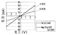
図2は、このようにして得られた本発明の発光素子のn側電極部分の電流・電圧特性を表すグラフ図である。同図においては、本発明によるパラジウム/金の積層構造の電極を形成した場合と、従来例としてチタン/金の積層構造を形成した場合とを比較して示した。図2から、n側電極として、パラジウムを採用した本発明の素子においては、良好なオーミック性を示し、その接触抵抗も従来の約1/4に低減したことが分かった。
【0032】
また、図3は、本発明の発光素子のp側電極部分の電流・電圧特性を表すグラフ図である。同図においては、本発明によるマグネシウム/パラジウム/ITOの積層構造の電極を形成した場合と、従来例としてニッケル/金の積層構造を形成した場合とを比較して示した。図3から、本発明の素子は、良好なオーミック性を示し、その接触抵抗も従来の約半分に低減していることが分かった。
【0033】
また、n側電極とp側電極のそれぞれに対して、金(Au)ワイアをボンディングした結果、電極の剥がれなどは見られず、電極の付着強度も十分に高いことが分かった。
【0034】
本発明の発光素子においては、20mAの電流に対する順方向電圧は3.4Vであり、光出力は91μWという良好な特性が得られた。さらに、ウェーハ面内でのI−V特性や光出力のばらつきも非常に少なく、素子歩留りは良好であった。
【0035】
次に、本発明の第2の実施の形態について説明する。
【0036】
図4は、本発明の第2の実施の形態に係る窒化ガリウム系化合物半導体発光素子の構造を例示する概略断面図である。すなわち、本実施形態の発光素子も、サファイア基板1上に積層された窒化ガリウム系半導体層2〜4からなる積層構造を有する。また、素子のp側には、p側電極と透明電極10とが積層され、電極パッド12に接続されている。また、n側においては、金属層5、6からなるn側電極が設けられている。前述した第1実施形態と同一の部分には、同一の符号を付して詳細な説明を省略する。
【0037】
ここで、本実施形態においては、p側電極の形成に際して、前述した第1実施形態の第1の金属層7と第2の金属層8とをそれぞれごく薄い膜厚で堆積する。ここでは、一例として、第1の金属層としてチタン(Ti)、第2の金属層としてマグネシウム(Mg)をそれぞれ用いた場合について例示する。
【0038】
すなわち、本実施形態においては、p側電極として、厚さ0.2mのチタン(Ti)層7’と、厚さ0.2mのマグネシウム(Mg)層8’と、厚さ5mのパラジウム(Pd)層9’とを積層する。このように、チタンやマグネシウムを極めて薄い膜厚で堆積した場合には、必ずしも連続的な薄膜とはならず、図4において一部拡大図として示したように、コンタクト層4の上に島状に形成される場合が多い。つまり、第1の金属層7’と第2の金属層9’とは、それぞれ島状に形成される。また、これらの金属層の堆積後に、アニールを施しても良く、また、半導体層と電極金属との間が十分に清浄な状態であれば、特にアニールはしなくても良い。ここで、アニールによって電極金属は合金化してもかまわないが半導体層と電極金属とが過剰に反応すると望ましくないため、アニール温度としては、500℃以下とすることが望ましい。
【0039】
このように、p側電極の形成に際して、第1の金属層と第2の金属層とを極めて薄く堆積した場合においても、付着強度は良好であり、且つ良好なオーミック性と低い接触抵抗とを実現することができる。これは、第1及び第2の金属層が有する付着強度の改善の作用と、第3の金属層が有するオーミック性の確保の作用とが維持された結果であると考えられる。
【0040】
次に、本発明の第3の実施の形態について説明する。
【0041】
図5は、本発明の第3の実施の形態に係る窒化ガリウム系化合物半導体発光素子の構造を例示する概略断面図である。すなわち、本実施形態の発光素子も、サファイア基板1上に積層された窒化ガリウム系半導体層2〜4からなる積層構造を有する。前述した第1実施形態と同一の部分には、同一の符号を付して詳細な説明を省略する。
【0042】
本実施形態においては、素子のp側においては、第1の金属層8と第2の金属層9と透明電極10とが形成されている。第1の金属層8の材料としては、チタン(Ti)、モリブデン(Mo)、タングステン(W)、マグネシウム(Mg)、金(Au)のうちのいずれかが用いられる。
【0043】
また、第2の金属層9の材料としては、パラジウム(Pd)、スカンジウム(Sc)、バナジュウム(V)、ジルコニウム(Zr)、ハフニウム(Hf)、タンタル(Ta)、ロジウム(Rh)、イリジウム(Ir)、コバルト(Co)、銅(Cu)、白金(Pt)、タングステン(W)のうちのいずれかが用いられる。
【0044】
ここでは、p側電極の第1の金属層8としてマグネシウム(Mg)、第2の金属層9としてパラジウム(Pd)層9、透明電極10としてITOをそれぞれ用いた場合を例示する。
【0045】
一方、素子のn側においては、第1の金属層13と第2の金属層5と第3の金属層6からなる3層構造の電極が形成されている。
【0046】
n側電極の第1の金属層13は、コンタクト層3との付着強度を確保する役割を有する。その材料としては、チタン(Ti)、ニッケル(Ni)、モリブデン(Mo)、タングステン(W)のうちのいずれかが用いられる。また、その層厚としては、5nm以下であることが望ましい。これよりも厚いと、接触抵抗が上昇し、電極の付着強度が低下する傾向がみられたからである。
【0047】
また、n側電極の第2の金属層5は、オーミック接触を確保する役割を有する。その材料としては、パラジウム(Pd)、スカンジウム(Sc)、バナジウム(V)、ジルコニウム(Zr)、ハフニウム(Hf)、タンタル(Ta)、ロジウム(Rh)、イリジウム(Ir)、コバルト(Co)、銅(Cu)のうちのいずれかが用いられる。
【0048】
また、n側電極の第3の金属層6としては、金(Au)が用いられる。
【0049】
ここでは、n側電極の第1の金属層13としてチタン(Ti)、第2の金属層5としてパラジウム(Pd)を用いた場合を例示する。
【0050】
このようにp側においてコンタクト層4にマグネシウム層8とパラジウム層9とを形成し、n側において、コンタクト層3にチタン層13とパラジウム層5とを形成した場合においても、p側とn側ともに良好なオーミック性と低い接触抵抗とを実現することができる。
【0051】
以上、具体例を参照しつつ本発明の実施の形態について説明した。しかし、本発明は、これらの具体例に限定されるものではない。例えば、前述した具体例においては、電極材料としてマグネシウム(Mg)、チタン(Ti)、パラジウム(Pd)、金(Au)を用い、また、透明電極としてITO、半導体層としてGaNをそれぞれ用いる場合を例示して説明したが、これらに限るものではない。すなわち、本発明によれば、p側とn側とにおいて、それぞれ、第1の金属層と第2の金属層とについて前述したいずれかの金属または、それらの合金を用いて同様の効果を得ることができる。
【0052】
また、それぞれの電極は、前述した2層または3層の積層構造に限定されず前述したいずれかの金属層からなる4層以上の積層構造であっても良い。
【0053】
また、透明電極として用いることができるものは、前述のITO以外にも、例えば、錫酸化物を用いても良く、または、金(Au)などの金属をごく薄く堆積したものを用いても良い。
【0054】
さらに、発光素子の構造としては、前述したもの以外にも、電極とのコンタクト部に窒化ガリウム系化合物半導体を用いたものであれば良く、各種の構造の発光ダイオードや半導体レーザなどについて同様に適用することができる。
【0055】
【発明の効果】
本発明は、以上説明したような形態で実施され、以下に説明する効果を奏する。
【0056】
まず、本発明によれば、窒化ガリウム系化合物半導体発光素子において、Alx Gay In1-x-y N(O≦x≦1、O≦y≦1、x+y≦1)からなる半導体に接触してチタン(Ti)やタングステン(W)等を含む、薄膜パラジウム(Pd)電極を形成することにより、p側電極、n側電極ともにオーミック特性を改善できる。
【0057】
ここで、p型の窒化ガリウム系化合物半導体層に対しては、この層に接触した5nm以下の薄いチタン(Ti)、タングステン(W)層等の薄膜金属層を設けることにより、電極と半導体層との密着性を向上させることができる。
【0058】
さらに、5nm以下の薄いマグネシウム(Mg)層、10nm以下の薄膜パラジウム(Pd)層、薄膜白金(Pt)層等の薄膜金属層を積層させることにより、良好なオーミック接触を得ることができる。
【0059】
さらに、ITO等の透明電極を積層させることにより薄膜電極のシート抵抗の低減をはかるとともに発光面内への均一な電流注入を実現することができる。
【0060】
一方、n型の窒化ガリウム系化合物半導体層に対しては、この層に接触して、5nm以下の薄いチタン(Ti)、ニッケル(Ni)層等により密着性を向上させ、さらにパラジウム(Pd)等の金属層により良好なオーミック特性を実現して、さらに金(Au)層を積層することにより、電極のシート抵抗を大幅に低減すると共に、ワイアボンディングを容易に実施することができるようになる。
【0061】
また、このような窒化ガリウム系化合物半導体発光素子を500℃以下の温度でアニールすることにより、電極金属と半導体層との過剰な反応を抑制しつつ電極の付着強度を改善し、コンタクト抵抗を低減することができる。
【0062】
さらに、本発明によれば、標準的なカップ型のリードフレームにマウントして、効率良く光を取り出すことができる。
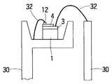
図6は、本発明の半導体発光素子をリードフレームにマウントした状態を表す概略図である。すなわち、本発明の半導体発光素子が、カップ型のリードフレーム30にマウントされ、ワイア32、32により接続されている。なお、同図においては、半導体発光素子の電極部の詳細な構造は、省略して表した。
本発明によれば、同図に表したように、広く用いられているカップ型のリードフレームを用いることができ、低いコストで、高い発光輝度の発光装置を容易に実現することができるようになる。
【0063】
以上説明したように本発明によれば、電極の半導体層への密着性向上、オーミック特性の改善、薄膜金属と透明電極の組み含わせによる外部量子効率の改善が実現され、産業上のメリットは多大である。
【図面の簡単な説明】
【図1】本発明の第1の実施の形態に係る窒化ガリウム系化合物半導体発光素子の構造を例示する概略断面図である。
【図2】本発明の発光素子のn側電極部分の電流・電圧特性を表すグラフ図である。
【図3】本発明の発光素子のp側電極部分の電流・電圧特性を表すグラフ図である。
【図4】本発明の第2の実施の形態に係る窒化ガリウム系化合物半導体発光素子の構造を例示する概略断面図である。
【図5】本発明の第3の実施の形態に係る窒化ガリウム系化合物半導体発光素子の構造を例示する概略断面図である。
【図6】本発明の半導体発光素子をリードフレームにマウントした状態を表す概略図である。
【図7】従来の窒化ガリウム系化合物半導体素子の構造例を表す概略図である。
【符号の説明】
1 サファイア基板
2 GaNバッファ層
3 n型GaN層
4 p型GaN層
5 第1の金属層
6 金(Au)層
7 第1の金属層
8 第2の金属層
9 第3の金属層
10 透明電極
11 絶縁膜
12 ボンディング用Ti/Au層
13 第1の金属層
14 n側電極
15 p側電極
16 導電性接着材料
17 リードフレーム
30 カップ型リードフレーム
32 ワイア
A リードフレーム間
B pn接合間[0001]
BACKGROUND OF THE INVENTION
The present invention relates to a gallium nitride compound semiconductor light emitting device and a method for manufacturing the same. More specifically, the present invention relates to a light emitting device in which a gallium nitride compound semiconductor layer such as GaN, InGaN, or GaAlN is laminated on a substrate, and a gallium nitride compound semiconductor light emitting device having an electrode having high adhesion strength and low contact resistance. The present invention relates to an element, a manufacturing method thereof, and a light emitting device.
[0002]
[Prior art]
In recent years, gallium nitride-based compound semiconductors represented by Al x Ga y In 1 -xy N (O ≦ x ≦ 1, O ≦ y ≦ 1, x + y ≦ 1) have been developed from the ultraviolet region to blue or green light emitting diodes (LEDs). It is attracting attention as a material. By using a compound semiconductor of such a material, it has become possible to emit ultraviolet light, blue light, green light, and the like with high light emission intensity, which has been difficult until now. Since such a gallium nitride compound semiconductor is generally grown on a sapphire substrate which is an insulating substrate, an electrode cannot be provided on the back surface of the substrate unlike a GaAs light emitting device. For this reason, it is necessary to form both the anode electrode and the cathode electrode on the side of the crystal grown semiconductor layer.
[0003]
In particular, in the case of a semiconductor device using a gallium nitride compound semiconductor, since the sapphire substrate has translucency with respect to the emission wavelength, a structure in which the electrode surface is mounted downward and light is extracted from the sapphire substrate side is used. It is common.
[0004]
FIG. 7 is a schematic view showing an example of the structure of a conventional gallium nitride compound semiconductor device. That is, in the light emitting device, the
[0005]
[Problems to be solved by the invention]
In the conventional semiconductor light emitting device as shown in FIG. 7, the light emitted when current is injected from the p-
[0006]
Furthermore, since it is required that the lead frame and the mounting position accuracy of the element be high, there is a problem that the mass productivity is lacking. In order to avoid these problems, it is sufficient to increase the element size and widen the distance between the lead frames 17 and 17. However, there arises a problem that the number of chips taken from the wafer is reduced and the cost is increased.
[0007]
On the other hand, in order to reduce the forward voltage of the light emitting element, the electrode and the gallium nitride semiconductor layer need to be in ohmic contact. Conventionally, an electrode containing aluminum (Al) is used as the n-side electrode, and an electrode containing nickel (Ni) or gold (Au) is used as the p-side electrode. However, the electrodes using these materials have not always obtained a preferable ohmic contact, but Al and Ni have infiltrated the GaN layer, leading to a decrease in reliability.
[0008]
The present invention has been made in view of such circumstances. That is, the purpose is to improve the adhesion of the electrode to the semiconductor layer, improve the ohmic characteristics, and improve the external quantum efficiency by combining a thin film metal and a transparent electrode, and a gallium nitride compound semiconductor light emitting device It is in providing the manufacturing method.
[0009]
According to one aspect of the present invention, an n-type semiconductor layer made of a nitride compound semiconductor;
An n-type electrode formed on the n-type semiconductor layer;
A p-type semiconductor layer formed on the n-type semiconductor layer separately from the n-type electrode;
A p-type electrode formed on the p-type semiconductor layer ,
The n-type electrode is
A first metal layer made of palladium (Pd) formed on the n-type semiconductor layer;
A second metal layer made of gold (Au) formed on the first metal layer,
The p-type electrode is
A third metal layer made of magnesium (Mg) formed on the p-type semiconductor layer;
A fourth metal layer made of palladium (Pd) formed on the third metal layer;
And a fifth metal layer made of ITO ( Indium Tin Oxide ) formed on the fourth metal layer. A gallium nitride compound semiconductor light emitting device is provided.
[0021]
According to the present invention, improvement in external quantum efficiency was achieved by improving electrode adhesion, improving ohmic characteristics, and combining a thin film metal and a transparent electrode. Also, it is not configured to mount with the electrode side down and extract light from the sapphire substrate side, so the conventional problems are short-circuiting between electrodes or junctions, significant reduction in yield during mounting, and long-term reliability. Problems such as deterioration of the property are solved. Furthermore, since a cup-type lead frame can be used, light can be extracted efficiently.
[0022]
DETAILED DESCRIPTION OF THE INVENTION
Embodiments of the present invention will be described below with reference to the drawings.
FIG. 1 is a schematic cross-sectional view illustrating the structure of a gallium nitride-based compound semiconductor light emitting device according to the first embodiment of the invention. That is, the light emitting device of the present invention has a laminated structure composed of gallium nitride based
[0023]
Here, as each material of the three
That is, the
The
The
Furthermore, by laminating the
[0024]
Here, a case where titanium (Ti) is used as the
[0025]
On the other hand, the
[0026]
Further, gold (Au) is used as the material of the
First, a
[0027]
Next, patterning is performed using the PEP method, and a palladium (Pd)
[0028]
Next, after patterning by the PEP method, a titanium (Ti)
[0029]
Next, flash annealing is performed at 450 ° C. for about 20 seconds in order to improve the adhesion and ohmic property between the p-side thin film electrode and the semiconductor layer and to improve the ohmic property of the n-side electrode. However, this flash annealing step may be unnecessary if the surface of the semiconductor layer is sufficiently clean without any oxide or the like.
[0030]
Next, after forming the
[0031]
FIG. 2 is a graph showing the current / voltage characteristics of the n-side electrode portion of the light emitting device of the present invention obtained as described above. In the figure, the case where the electrode of the palladium / gold laminated structure according to the present invention is formed and the case where the titanium / gold laminated structure is formed as a conventional example are compared and shown. From FIG. 2, it was found that the element of the present invention employing palladium as the n-side electrode showed good ohmic properties and its contact resistance was reduced to about 1/4 of the conventional one.
[0032]
FIG. 3 is a graph showing the current / voltage characteristics of the p-side electrode portion of the light emitting device of the present invention. In the figure, the case of forming an electrode having a magnesium / palladium / ITO laminate structure according to the present invention is compared with the case of forming a nickel / gold laminate structure as a conventional example. From FIG. 3, it was found that the device of the present invention showed a good ohmic property, and its contact resistance was reduced to about half that of the prior art.
[0033]
Further, as a result of bonding gold (Au) wire to each of the n-side electrode and the p-side electrode, it was found that no peeling of the electrode was observed and the adhesion strength of the electrode was sufficiently high.
[0034]
In the light emitting device of the present invention, the forward voltage with respect to the current of 20 mA was 3.4 V, and the light output had good characteristics of 91 μW. Furthermore, there were very few variations in IV characteristics and light output within the wafer surface, and the device yield was good.
[0035]
Next, a second embodiment of the present invention will be described.
[0036]
FIG. 4 is a schematic cross-sectional view illustrating the structure of a gallium nitride compound semiconductor light emitting device according to the second embodiment of the invention. That is, the light emitting device of this embodiment also has a stacked structure including gallium nitride based
[0037]
Here, in the present embodiment, when the p-side electrode is formed, the
[0038]
That is, in this embodiment, as the p-side electrode, a titanium (Ti)
[0039]
Thus, even when the first metal layer and the second metal layer are deposited extremely thin when forming the p-side electrode, the adhesion strength is good, and good ohmic properties and low contact resistance are obtained. Can be realized. This is considered to be a result of maintaining the action of improving the adhesion strength of the first and second metal layers and the action of ensuring the ohmic property of the third metal layer.
[0040]
Next, a third embodiment of the present invention will be described.
[0041]
FIG. 5 is a schematic cross-sectional view illustrating the structure of a gallium nitride compound semiconductor light emitting device according to the third embodiment of the invention. That is, the light emitting device of this embodiment also has a stacked structure including gallium nitride based
[0042]
In the present embodiment, the
[0043]
The material of the
[0044]
Here, a case where magnesium (Mg) is used as the
[0045]
On the other hand, on the n-side of the element, an electrode having a three-layer structure including the
[0046]
The
[0047]
In addition, the
[0048]
Further, as the
[0049]
Here, a case where titanium (Ti) is used as the
[0050]
Thus, even when the
[0051]
The embodiments of the present invention have been described above with reference to specific examples. However, the present invention is not limited to these specific examples. For example, in the specific example described above, magnesium (Mg), titanium (Ti), palladium (Pd), and gold (Au) are used as electrode materials, ITO is used as a transparent electrode, and GaN is used as a semiconductor layer. Although illustrated and demonstrated, it is not restricted to these. That is, according to the present invention, on the p side and the n side, the same effect can be obtained by using any of the metals described above for the first metal layer and the second metal layer, or an alloy thereof. be able to.
[0052]
In addition, each electrode is not limited to the above-described two-layer or three-layer stack structure, and may have a four-layer or more stack structure including any of the metal layers described above.
[0053]
In addition to the above-described ITO, for example, tin oxide may be used as the transparent electrode, or a thinly deposited metal such as gold (Au) may be used. .
[0054]
Further, the structure of the light emitting element is not limited to that described above as long as it uses a gallium nitride compound semiconductor for the contact portion with the electrode, and the same applies to light emitting diodes and semiconductor lasers having various structures. can do.
[0055]
【The invention's effect】
The present invention is implemented in the form as described above, and has the effects described below.
[0056]
First, according to the present invention, in a gallium nitride-based compound semiconductor light emitting device, a semiconductor made of Al x Ga y In 1-xy N (O ≦ x ≦ 1, O ≦ y ≦ 1, x + y ≦ 1) is contacted. By forming a thin film palladium (Pd) electrode containing titanium (Ti), tungsten (W), or the like, ohmic characteristics can be improved for both the p-side electrode and the n-side electrode.
[0057]
Here, for the p-type gallium nitride compound semiconductor layer, an electrode and a semiconductor layer are formed by providing a thin metal layer of 5 nm or less, such as a thin titanium (Ti) or tungsten (W) layer, in contact with this layer. Adhesiveness can be improved.
[0058]
Furthermore, a good ohmic contact can be obtained by laminating a thin film metal layer such as a thin magnesium (Mg) layer of 5 nm or less, a thin film palladium (Pd) layer of 10 nm or less, or a thin film platinum (Pt) layer.
[0059]
Furthermore, by laminating transparent electrodes such as ITO, it is possible to reduce the sheet resistance of the thin film electrode and to achieve uniform current injection into the light emitting surface.
[0060]
On the other hand, for an n-type gallium nitride compound semiconductor layer, contact with this layer improves adhesion with a thin titanium (Ti), nickel (Ni) layer or the like of 5 nm or less, and further, palladium (Pd). By realizing good ohmic characteristics with a metal layer such as a metal layer and further laminating a gold (Au) layer, the sheet resistance of the electrode can be greatly reduced and wire bonding can be easily performed. .
[0061]
Also, by annealing such a gallium nitride-based compound semiconductor light emitting device at a temperature of 500 ° C. or lower, the adhesion strength of the electrode is improved and the contact resistance is reduced while suppressing an excessive reaction between the electrode metal and the semiconductor layer. can do.
[0062]
Furthermore, according to the present invention, light can be efficiently extracted by mounting on a standard cup-type lead frame.
FIG. 6 is a schematic view showing a state in which the semiconductor light emitting device of the present invention is mounted on a lead frame. That is, the semiconductor light emitting device of the present invention is mounted on a cup-
According to the present invention, as shown in the figure, a widely used cup-type lead frame can be used, and a light emitting device with high luminance can be easily realized at low cost. Become.
[0063]
As described above, according to the present invention, the adhesion of the electrode to the semiconductor layer, the improvement of ohmic characteristics, and the improvement of external quantum efficiency by the combination of the thin film metal and the transparent electrode are realized, and the industrial merit is It is a great deal.
[Brief description of the drawings]
FIG. 1 is a schematic cross-sectional view illustrating the structure of a gallium nitride-based compound semiconductor light emitting device according to a first embodiment of the invention.
FIG. 2 is a graph showing current / voltage characteristics of an n-side electrode portion of the light emitting device of the present invention.
FIG. 3 is a graph showing current / voltage characteristics of the p-side electrode portion of the light emitting device of the present invention.
FIG. 4 is a schematic cross-sectional view illustrating the structure of a gallium nitride-based compound semiconductor light emitting device according to a second embodiment of the invention.
FIG. 5 is a schematic cross-sectional view illustrating the structure of a gallium nitride-based compound semiconductor light emitting element according to a third embodiment of the invention.
FIG. 6 is a schematic view showing a state in which the semiconductor light emitting device of the present invention is mounted on a lead frame.
FIG. 7 is a schematic view showing a structural example of a conventional gallium nitride compound semiconductor device.
[Explanation of symbols]
DESCRIPTION OF
Claims (1)
前記n型半導体層の上に形成されるn型電極と、
前記n型半導体層の上に、前記n型電極と分離して形成されるp型半導体層と、
前記p型半導体層の上に形成されるp型電極と、を備え、
前記n型電極は、
前記n型半導体層の上に形成されるパラジウム(Pd)からなる第1の金属層と、
前記第1の金属層の上に形成される金(Au)からなる第2の金属層と、を有し、
前記p型電極は、
前記p型半導体層の上に形成されるマグネシウム(Mg)からなる第3の金属層と、
前記第3の金属層の上に形成されるパラジウム(Pd)からなる第4の金属層と、
前記第4の金属層の上に形成されるITO( Indium Tin Oxide )からなる第5の金属層と、を有することを特徴とする窒化ガリウム系化合物半導体発光素子。An n-type semiconductor layer made of a nitride compound semiconductor;
An n-type electrode formed on the n-type semiconductor layer;
A p-type semiconductor layer formed on the n-type semiconductor layer separately from the n-type electrode;
A p-type electrode formed on the p-type semiconductor layer ,
The n-type electrode is
A first metal layer made of palladium (Pd) formed on the n-type semiconductor layer;
A second metal layer made of gold (Au) formed on the first metal layer,
The p-type electrode is
A third metal layer made of magnesium (Mg) formed on the p-type semiconductor layer;
A fourth metal layer made of palladium (Pd) formed on the third metal layer;
And a fifth metal layer made of ITO ( Indium Tin Oxide ) formed on the fourth metal layer .
Priority Applications (2)
| Application Number | Priority Date | Filing Date | Title |
|---|---|---|---|
| JP07747798A JP4183299B2 (en) | 1998-03-25 | 1998-03-25 | Gallium nitride compound semiconductor light emitting device |
| US09/261,819 US5990500A (en) | 1998-03-25 | 1999-03-03 | Nitride compound semiconductor light emitting element and its manufacturing method |
Applications Claiming Priority (1)
| Application Number | Priority Date | Filing Date | Title |
|---|---|---|---|
| JP07747798A JP4183299B2 (en) | 1998-03-25 | 1998-03-25 | Gallium nitride compound semiconductor light emitting device |
Publications (2)
| Publication Number | Publication Date |
|---|---|
| JPH11274562A JPH11274562A (en) | 1999-10-08 |
| JP4183299B2 true JP4183299B2 (en) | 2008-11-19 |
Family
ID=13635078
Family Applications (1)
| Application Number | Title | Priority Date | Filing Date |
|---|---|---|---|
| JP07747798A Expired - Fee Related JP4183299B2 (en) | 1998-03-25 | 1998-03-25 | Gallium nitride compound semiconductor light emitting device |
Country Status (2)
| Country | Link |
|---|---|
| US (1) | US5990500A (en) |
| JP (1) | JP4183299B2 (en) |
Families Citing this family (76)
| Publication number | Priority date | Publication date | Assignee | Title |
|---|---|---|---|---|
| US6291840B1 (en) * | 1996-11-29 | 2001-09-18 | Toyoda Gosei Co., Ltd. | GaN related compound semiconductor light-emitting device |
| JPH10247747A (en) * | 1997-03-05 | 1998-09-14 | Toshiba Corp | Semiconductor light emitting device and manufacture thereof |
| US6936859B1 (en) * | 1998-05-13 | 2005-08-30 | Toyoda Gosei Co., Ltd. | Light-emitting semiconductor device using group III nitride compound |
| US6262440B1 (en) * | 1998-06-29 | 2001-07-17 | Philips Electronics North America Corp. | Metal electrical contact for high current density applications in LED and laser devices |
| JP3469484B2 (en) * | 1998-12-24 | 2003-11-25 | 株式会社東芝 | Semiconductor light emitting device and method of manufacturing the same |
| JP2000252230A (en) * | 1998-12-28 | 2000-09-14 | Sanyo Electric Co Ltd | Semiconductor element and its manufacture |
| US6876003B1 (en) * | 1999-04-15 | 2005-04-05 | Sumitomo Electric Industries, Ltd. | Semiconductor light-emitting device, method of manufacturing transparent conductor film and method of manufacturing compound semiconductor light-emitting device |
| KR100525494B1 (en) | 1999-04-26 | 2005-11-01 | 샤프 가부시키가이샤 | Electrode structure on p-type ⅲ group nitride semiconductor layer and formation method thereof |
| US6803603B1 (en) * | 1999-06-23 | 2004-10-12 | Kabushiki Kaisha Toshiba | Semiconductor light-emitting element |
| US7211877B1 (en) * | 1999-09-13 | 2007-05-01 | Vishay-Siliconix | Chip scale surface mount package for semiconductor device and process of fabricating the same |
| US6812502B1 (en) * | 1999-11-04 | 2004-11-02 | Uni Light Technology Incorporation | Flip-chip light-emitting device |
| US7595547B1 (en) | 2005-06-13 | 2009-09-29 | Vishay-Siliconix | Semiconductor die package including cup-shaped leadframe |
| US6744124B1 (en) * | 1999-12-10 | 2004-06-01 | Siliconix Incorporated | Semiconductor die package including cup-shaped leadframe |
| US6992334B1 (en) * | 1999-12-22 | 2006-01-31 | Lumileds Lighting U.S., Llc | Multi-layer highly reflective ohmic contacts for semiconductor devices |
| JP2001217456A (en) * | 2000-02-03 | 2001-08-10 | Sharp Corp | Gallium nitride system compound semiconductor light- emitting device |
| JP4026294B2 (en) * | 2000-03-07 | 2007-12-26 | 豊田合成株式会社 | Method for producing group III nitride compound semiconductor device |
| US6526082B1 (en) * | 2000-06-02 | 2003-02-25 | Lumileds Lighting U.S., Llc | P-contact for GaN-based semiconductors utilizing a reverse-biased tunnel junction |
| JP4024994B2 (en) * | 2000-06-30 | 2007-12-19 | 株式会社東芝 | Semiconductor light emitting device |
| DE10060439A1 (en) * | 2000-12-05 | 2002-06-13 | Osram Opto Semiconductors Gmbh | Contact metallization used in production of semiconductors contains copper distributed in partial volume |
| US6608360B2 (en) * | 2000-12-15 | 2003-08-19 | University Of Houston | One-chip micro-integrated optoelectronic sensor |
| US6888171B2 (en) * | 2000-12-22 | 2005-05-03 | Dallan Luming Science & Technology Group Co., Ltd. | Light emitting diode |
| JP4148664B2 (en) * | 2001-02-02 | 2008-09-10 | 三洋電機株式会社 | Nitride-based semiconductor laser device and method for forming the same |
| JP5283293B2 (en) * | 2001-02-21 | 2013-09-04 | ソニー株式会社 | Semiconductor light emitting device |
| JP3772098B2 (en) | 2001-05-15 | 2006-05-10 | シャープ株式会社 | Nitride semiconductor light emitting device |
| JP3912044B2 (en) * | 2001-06-06 | 2007-05-09 | 豊田合成株式会社 | Method for manufacturing group III nitride compound semiconductor light emitting device |
| TW543128B (en) * | 2001-07-12 | 2003-07-21 | Highlink Technology Corp | Surface mounted and flip chip type LED package |
| US6744075B2 (en) | 2001-09-17 | 2004-06-01 | Sanyo Electric Co., Ltd. | Nitride-based semiconductor light-emitting device and method of forming the same |
| TW588204B (en) * | 2002-03-14 | 2004-05-21 | Wintek Corp | Transparent conduction plate having low junction resistance and manufacturing method thereof |
| US8294172B2 (en) * | 2002-04-09 | 2012-10-23 | Lg Electronics Inc. | Method of fabricating vertical devices using a metal support film |
| JP2004006498A (en) * | 2002-05-31 | 2004-01-08 | Toyoda Gosei Co Ltd | Group iii nitride based compound semiconductor light emitting element |
| US20030222263A1 (en) * | 2002-06-04 | 2003-12-04 | Kopin Corporation | High-efficiency light-emitting diodes |
| US6841802B2 (en) | 2002-06-26 | 2005-01-11 | Oriol, Inc. | Thin film light emitting diode |
| JP4507532B2 (en) | 2002-08-27 | 2010-07-21 | 日亜化学工業株式会社 | Nitride semiconductor device |
| KR100543696B1 (en) * | 2002-09-09 | 2006-01-20 | 삼성전기주식회사 | Light emitting diode with high efficiency |
| TWI243488B (en) * | 2003-02-26 | 2005-11-11 | Osram Opto Semiconductors Gmbh | Electrical contact-area for optoelectronic semiconductor-chip and its production method |
| JP4519423B2 (en) * | 2003-05-30 | 2010-08-04 | 創世理工株式会社 | Optical devices using semiconductors |
| KR100561841B1 (en) * | 2003-08-23 | 2006-03-16 | 삼성전자주식회사 | Transparant Film Electrode for Ohmic Contact of p-Type Semiconductor Comprising N, Ga for High-quality Light Emitting Diodes and Laser Diodes |
| KR100624411B1 (en) * | 2003-08-25 | 2006-09-18 | 삼성전자주식회사 | light emitting device and method of manufacturing the same |
| US20050070097A1 (en) * | 2003-09-29 | 2005-03-31 | International Business Machines Corporation | Atomic laminates for diffusion barrier applications |
| US7417264B2 (en) * | 2003-12-22 | 2008-08-26 | Samsung Electronics Co., Ltd. | Top-emitting nitride-based light emitting device and method of manufacturing the same |
| KR100506741B1 (en) * | 2003-12-24 | 2005-08-08 | 삼성전기주식회사 | Nitride semiconductor light emitting device for flip chip and method of manufacturing the same |
| TWI224877B (en) * | 2003-12-25 | 2004-12-01 | Super Nova Optoelectronics Cor | Gallium nitride series light-emitting diode structure and its manufacturing method |
| US7960746B2 (en) * | 2004-01-06 | 2011-06-14 | Samsung Led Co., Ltd. | Low resistance electrode and compound semiconductor light emitting device including the same |
| KR100586948B1 (en) * | 2004-01-19 | 2006-06-07 | 삼성전기주식회사 | Nitride semiconductor light emitting device |
| KR100601945B1 (en) | 2004-03-10 | 2006-07-14 | 삼성전자주식회사 | Top emitting light emitting device and method of manufacturing thereof |
| KR100634503B1 (en) * | 2004-03-12 | 2006-10-16 | 삼성전자주식회사 | Light emitting device and method of manufacturing thereof |
| EP1746664B1 (en) * | 2004-03-31 | 2017-05-17 | Nichia Corporation | Nitride semiconductor light emitting element |
| KR100611491B1 (en) * | 2004-08-26 | 2006-08-10 | 엘지이노텍 주식회사 | Nitride semiconductor LED and fabrication method thereof |
| US7215031B2 (en) * | 2004-11-10 | 2007-05-08 | Oki Electric Industry Co., Ltd. | Multi chip package |
| CN100358167C (en) * | 2004-12-17 | 2007-12-26 | 北京工业大学 | GaN base LED high reflectance electrode |
| JP4603370B2 (en) * | 2005-01-18 | 2010-12-22 | 創世理工株式会社 | Semiconductor optical device fabricated on substrate and fabrication method thereof |
| JP5089020B2 (en) * | 2005-01-19 | 2012-12-05 | 創世理工株式会社 | Semiconductor electronic devices fabricated on a substrate |
| JP3949157B2 (en) * | 2005-04-08 | 2007-07-25 | 三菱電線工業株式会社 | Semiconductor device and manufacturing method thereof |
| KR100878433B1 (en) * | 2005-05-18 | 2009-01-13 | 삼성전기주식회사 | Fablication methodes of ohmic contact layer and light emitting device adopting the layer |
| JP5138873B2 (en) | 2005-05-19 | 2013-02-06 | 日亜化学工業株式会社 | Nitride semiconductor device |
| JP4030556B2 (en) * | 2005-06-30 | 2008-01-09 | シャープ株式会社 | Nitride semiconductor laser device and nitride semiconductor laser device |
| JP5067158B2 (en) * | 2005-07-08 | 2012-11-07 | 日本電気株式会社 | Electrode structure, semiconductor element, and manufacturing method thereof |
| KR101041843B1 (en) | 2005-07-30 | 2011-06-17 | 삼성엘이디 주식회사 | Nitride-based compound semiconductor light emitting device and fabrication method of the same |
| EP1821347B1 (en) * | 2006-02-16 | 2018-01-03 | LG Electronics Inc. | Light emitting device having vertical structure and method for manufacturing the same |
| KR100833489B1 (en) * | 2006-02-21 | 2008-05-29 | 한국전자통신연구원 | Transparent contact electrode for Si nanocrystal light-emitting diodes, and method of fabricating |
| GB2446611B (en) * | 2007-02-14 | 2011-08-17 | Bookham Technology Plc | Low creep metallization for optoelectronic applications |
| JP5077068B2 (en) * | 2007-05-30 | 2012-11-21 | 日亜化学工業株式会社 | Nitride semiconductor device and manufacturing method thereof |
| TWI341600B (en) * | 2007-08-31 | 2011-05-01 | Huga Optotech Inc | Light optoelectronic device and forming method thereof |
| WO2010052810A1 (en) * | 2008-11-06 | 2010-05-14 | パナソニック株式会社 | Nitride semiconductor element and method for manufacturing the same |
| EP2273573A4 (en) * | 2009-03-11 | 2012-11-14 | Panasonic Corp | Nitride semiconductor element and method for manufacturing same |
| JP5498723B2 (en) * | 2009-04-10 | 2014-05-21 | スタンレー電気株式会社 | Zinc oxide based semiconductor device and method for manufacturing the same |
| JP5502360B2 (en) * | 2009-04-10 | 2014-05-28 | スタンレー電気株式会社 | Zinc oxide based semiconductor device and method for manufacturing the same |
| EP2479807B1 (en) * | 2009-12-25 | 2014-06-18 | Panasonic Corporation | Nitride semiconductor light emitting diode |
| JP4843123B2 (en) | 2010-04-01 | 2011-12-21 | パナソニック株式会社 | Nitride-based semiconductor device and manufacturing method thereof |
| JP5776021B2 (en) * | 2010-04-02 | 2015-09-09 | パナソニックIpマネジメント株式会社 | Nitride-based semiconductor device and light source |
| EP2565942B1 (en) * | 2010-04-28 | 2018-10-24 | Panasonic Intellectual Property Management Co., Ltd. | Nitride-type semiconductor element |
| JP5685035B2 (en) * | 2010-09-24 | 2015-03-18 | 住友電気工業株式会社 | Manufacturing method of semiconductor light emitting device |
| JP5232338B2 (en) * | 2011-04-08 | 2013-07-10 | パナソニック株式会社 | Nitride-based semiconductor device and manufacturing method thereof |
| CN106328781B (en) * | 2016-11-03 | 2018-12-11 | 湘能华磊光电股份有限公司 | High reflectance LED electrode and preparation method thereof |
| JP2019134119A (en) * | 2018-02-01 | 2019-08-08 | 豊田合成株式会社 | Group-iii nitride semiconductor light-emitting element |
| WO2022174426A1 (en) * | 2021-02-20 | 2022-08-25 | 厦门三安光电有限公司 | Semiconductor light-emitting element and method for manufacturing same |
Family Cites Families (3)
| Publication number | Priority date | Publication date | Assignee | Title |
|---|---|---|---|---|
| US5740192A (en) * | 1994-12-19 | 1998-04-14 | Kabushiki Kaisha Toshiba | Semiconductor laser |
| JP3457468B2 (en) * | 1995-09-12 | 2003-10-20 | 株式会社東芝 | Multilayer semiconductor device |
| JP2941743B2 (en) * | 1996-06-05 | 1999-08-30 | 株式会社東芝 | Compound semiconductor light emitting device and method of manufacturing the same |
-
1998
- 1998-03-25 JP JP07747798A patent/JP4183299B2/en not_active Expired - Fee Related
-
1999
- 1999-03-03 US US09/261,819 patent/US5990500A/en not_active Expired - Lifetime
Also Published As
| Publication number | Publication date |
|---|---|
| US5990500A (en) | 1999-11-23 |
| JPH11274562A (en) | 1999-10-08 |
Similar Documents
| Publication | Publication Date | Title |
|---|---|---|
| JP4183299B2 (en) | Gallium nitride compound semiconductor light emitting device | |
| TWI274429B (en) | Semiconductor light-emitting device and manufacturing method thereof | |
| US8552455B2 (en) | Semiconductor light-emitting diode and a production method therefor | |
| JP4449405B2 (en) | Nitride semiconductor light emitting device and manufacturing method thereof | |
| JP5092419B2 (en) | GaN-based light emitting diode element | |
| JP7049186B2 (en) | Manufacturing method of semiconductor light emitting device and semiconductor light emitting device | |
| JP4159865B2 (en) | Nitride compound semiconductor light emitting device manufacturing method | |
| JP2697572B2 (en) | Gallium nitride based compound semiconductor light emitting device | |
| JP3207773B2 (en) | Compound semiconductor light emitting device and method of manufacturing the same | |
| JP2000294837A (en) | Gallium nitride compound semiconductor light emitting element | |
| JP2001217456A (en) | Gallium nitride system compound semiconductor light- emitting device | |
| JPH09232632A (en) | Semiconductor light-emitting element and manufacture thereof | |
| JP5608589B2 (en) | Semiconductor light emitting device and method for manufacturing semiconductor light emitting device | |
| WO2011077748A1 (en) | Vertical group iii nitride semiconductor light-emitting element and production method therefor | |
| KR20080053180A (en) | Supporting substrates for semiconductor light emitting device and high-performance vertical structured semiconductor light emitting devices using the supporting substrates | |
| JP2005011857A (en) | Nitride semiconductor light emitting device | |
| JP4868821B2 (en) | Gallium nitride compound semiconductor and light emitting device | |
| TWI568024B (en) | Nitride semiconductor light emitting device and manufacturing method thereof | |
| US6653215B1 (en) | Contact to n-GaN with Au termination | |
| KR101510382B1 (en) | fabrication of vertical structured light emitting diodes using group 3 nitride-based semiconductors and its related methods | |
| JP2004319672A (en) | Light emitting diode | |
| JP2941743B2 (en) | Compound semiconductor light emitting device and method of manufacturing the same | |
| JP5438534B2 (en) | Semiconductor device and manufacturing method thereof | |
| JP4312504B2 (en) | Electrode of light emitting diode element and light emitting diode element | |
| JP4985930B2 (en) | Nitride-based compound semiconductor light-emitting device and method for manufacturing the same |
Legal Events
| Date | Code | Title | Description |
|---|---|---|---|
| A521 | Written amendment |
Free format text: JAPANESE INTERMEDIATE CODE: A523 Effective date: 20040922 |
|
| A621 | Written request for application examination |
Free format text: JAPANESE INTERMEDIATE CODE: A621 Effective date: 20040922 |
|
| A977 | Report on retrieval |
Free format text: JAPANESE INTERMEDIATE CODE: A971007 Effective date: 20070316 |
|
| A131 | Notification of reasons for refusal |
Free format text: JAPANESE INTERMEDIATE CODE: A131 Effective date: 20070508 |
|
| A521 | Written amendment |
Free format text: JAPANESE INTERMEDIATE CODE: A523 Effective date: 20070709 |
|
| A131 | Notification of reasons for refusal |
Free format text: JAPANESE INTERMEDIATE CODE: A131 Effective date: 20080311 |
|
| A521 | Written amendment |
Free format text: JAPANESE INTERMEDIATE CODE: A523 Effective date: 20080512 |
|
| TRDD | Decision of grant or rejection written | ||
| A01 | Written decision to grant a patent or to grant a registration (utility model) |
Free format text: JAPANESE INTERMEDIATE CODE: A01 Effective date: 20080826 |
|
| A01 | Written decision to grant a patent or to grant a registration (utility model) |
Free format text: JAPANESE INTERMEDIATE CODE: A01 |
|
| A61 | First payment of annual fees (during grant procedure) |
Free format text: JAPANESE INTERMEDIATE CODE: A61 Effective date: 20080902 |
|
| FPAY | Renewal fee payment (event date is renewal date of database) |
Free format text: PAYMENT UNTIL: 20110912 Year of fee payment: 3 |
|
| FPAY | Renewal fee payment (event date is renewal date of database) |
Free format text: PAYMENT UNTIL: 20110912 Year of fee payment: 3 |
|
| FPAY | Renewal fee payment (event date is renewal date of database) |
Free format text: PAYMENT UNTIL: 20110912 Year of fee payment: 3 |
|
| FPAY | Renewal fee payment (event date is renewal date of database) |
Free format text: PAYMENT UNTIL: 20120912 Year of fee payment: 4 |
|
| FPAY | Renewal fee payment (event date is renewal date of database) |
Free format text: PAYMENT UNTIL: 20120912 Year of fee payment: 4 |
|
| FPAY | Renewal fee payment (event date is renewal date of database) |
Free format text: PAYMENT UNTIL: 20130912 Year of fee payment: 5 |
|
| LAPS | Cancellation because of no payment of annual fees |