EP1821091A1 - Verfahren zur Herstellung von elektronischen Bauelementen und Drucksensor - Google Patents
Verfahren zur Herstellung von elektronischen Bauelementen und Drucksensor Download PDFInfo
- Publication number
- EP1821091A1 EP1821091A1 EP06002983A EP06002983A EP1821091A1 EP 1821091 A1 EP1821091 A1 EP 1821091A1 EP 06002983 A EP06002983 A EP 06002983A EP 06002983 A EP06002983 A EP 06002983A EP 1821091 A1 EP1821091 A1 EP 1821091A1
- Authority
- EP
- European Patent Office
- Prior art keywords
- metal layer
- wafer
- electronic components
- areas
- electronic component
- Prior art date
- Legal status (The legal status is an assumption and is not a legal conclusion. Google has not performed a legal analysis and makes no representation as to the accuracy of the status listed.)
- Granted
Links
Images


Classifications
-
- G—PHYSICS
- G01—MEASURING; TESTING
- G01L—MEASURING FORCE, STRESS, TORQUE, WORK, MECHANICAL POWER, MECHANICAL EFFICIENCY, OR FLUID PRESSURE
- G01L19/00—Details of, or accessories for, apparatus for measuring steady or quasi-steady pressure of a fluent medium insofar as such details or accessories are not special to particular types of pressure gauges
- G01L19/14—Housings
- G01L19/147—Details about the mounting of the sensor to support or covering means
-
- G—PHYSICS
- G01—MEASURING; TESTING
- G01L—MEASURING FORCE, STRESS, TORQUE, WORK, MECHANICAL POWER, MECHANICAL EFFICIENCY, OR FLUID PRESSURE
- G01L19/00—Details of, or accessories for, apparatus for measuring steady or quasi-steady pressure of a fluent medium insofar as such details or accessories are not special to particular types of pressure gauges
- G01L19/14—Housings
- G01L19/145—Housings with stress relieving means
- G01L19/146—Housings with stress relieving means using flexible element between the transducer and the support
-
- G—PHYSICS
- G01—MEASURING; TESTING
- G01L—MEASURING FORCE, STRESS, TORQUE, WORK, MECHANICAL POWER, MECHANICAL EFFICIENCY, OR FLUID PRESSURE
- G01L9/00—Measuring steady of quasi-steady pressure of fluid or fluent solid material by electric or magnetic pressure-sensitive elements; Transmitting or indicating the displacement of mechanical pressure-sensitive elements, used to measure the steady or quasi-steady pressure of a fluid or fluent solid material, by electric or magnetic means
- G01L9/0041—Transmitting or indicating the displacement of flexible diaphragms
- G01L9/0042—Constructional details associated with semiconductive diaphragm sensors, e.g. etching, or constructional details of non-semiconductive diaphragms
Definitions
- the invention relates to a method for producing electronic components, in particular for the production of electronic sensors for pressure and / or differential pressure measurement according to the features specified in the preamble of claim 1 and such an electronic component according to the features specified in the preamble of claim 5.
- Electronic components in particular for use as a pressure or differential pressure sensor, for example DE 297 24 622 U1 known. They consist of a semiconductor substrate, which is thinned out in the region which is to form the later membrane region of the sensor. In this area, the actual measuring elements in the form of resistors are formed, which are typically connected to a measuring bridge and change their resistance properties in later use due to the membrane elongation, which in turn is used as a measure of the upcoming pressure for electronic evaluation.
- the silicon substrate and the measuring elements formed therein are respectively provided on the top and bottom of the substrate with an insulating layer, typically an oxide layer, which in turn is coated with a corrosion-resistant metal layer, typically a chromium-tantalum layer. This metal layer extends in known components on both sides to the edge and is interrupted only in the region of the connection contacts.
- Such electronic components are not manufactured individually, but typically in the form of wafers, i. a plurality of electronic components are formed next to one another in the silicon substrate or on the silicon substrate, after which the insulating layer is applied and finally the protective metal layer is applied. The thus formed plurality of electronic components is then mechanically separated into individual components. This method has long been used in semiconductor technology and has proven itself.
- the invention has the object, a generic method in such a way that the aforementioned disadvantages are reduced, in particular the possibly triggered leakage currents are prevented.
- the inventive method provides that the semiconductor structures of the electronic components are first generated on a wafer, after which at least one insulating layer, for. B. an oxide layer and subsequently at least one protective metal layer is applied.
- the metal layer is applied in sections and only in those areas of the wafer in which later no division of the wafer takes place.
- it can alternatively be applied over the entire surface of the wafer, for example by vapor deposition, after which the metal layer is removed prior to the division, at least in the regions in which the wafer is subsequently divided. In both methods, it is thus always ensured that no metal layer is present in the regions of the later parting lines before the wafer is cut. Thereafter, the electronic components thus formed are released by cutting the wafer from the composite.
- the basic idea of the present invention is thus, in the areas in which the wafer is divided to form the individual electronic components after the successful manufacturing process, not with a To provide metal layer or there to remove the metal layer targeted, so that no later cutting of the wafer and no metal layer must be severed.
- This has the advantage that the metal layer does not have to be divided and thus also does not occur at the outset described adverse effects, which lead to a comparatively large tolerance of the electrical properties of the electronic components thus formed.
- the method according to the invention thus makes it possible, by the targeted application of the metal layer only in the areas in which later no division of the wafer more, to significantly reduce the tolerance of the electrical properties of the components thus formed and thus to increase the quality of the components, without the manufacturing process noticeably more expensive or expensive to make, since the metal layer anyway not opaque, but always sections must be provided, since, for example, in the field of electrical contacts anyway already had a recess must be provided.
- the entire surface of the wafer by vapor deposition with a metal layer and then to remove these sections in sections by chemical or electrochemical process, advantageously by etching.
- the removal of the metal layer in sections may alternatively also be effected by suitable thermal action, for example by laser radiation.
- the areas in which the subsequent division of the wafer takes place are advantageously covered by masking before the metal layer is applied.
- the masking ensures that the metal layer does not adhere, so that no metal layer is applied in the masked areas.
- the metal layer terminates at a sufficient distance from the later parting line or at the end face then formed there on the circumference, then a further processing of these narrow end faces formed by the separation can basically be dispensed with. If, however, for reasons of space, for example, the remaining distance of the metal layer to the parting line is comparatively low, then it may be particularly advantageous if, after the wafer has been cut, the end sides formed by the parting are sealed, for example by a hardening liquid seal applied during application has electrically insulating effect.
- This seal not only protects the narrow end faces of the respective component formed by the separation, but also ensures that any damage, in particular microscopic breakouts, in the edge region of the insulating layer are filled, so that no appreciable leakage currents can form in this region.
- the electronic component according to the invention thus formed is characterized in that its protective metal layer, which is at least on one side, ends on all sides at a distance from the nearest peripheral edge. It is understood that the distance to the nearest circumferential edge on the one hand chosen so small that is ensured in each case that the area to be protected, in a differential pressure or pressure sensor, this is typically the membrane area and the surrounding clamping area, protected by the metal layer on the other hand, is so large that it is ensured that the subsequent separation process takes place outside the metal layer.
- a protective metal layer is provided on both sides, which not only the membrane itself, but also the immediate adjacent area, advantageously extending beyond the clamping point, so that the device is reliably protected against external influences. Clamping in the aforementioned sense is not necessarily the point at which the device is mechanically held, but the point at which the component is sealed against the medium whose pressure or differential pressure is to be measured.
- a seal is expediently designed in such a way that it can be applied in liquid form and, after curing / drying, forms an electrically insulating and possibly also the substrate which protects against external influences.
- the invention is not limited to a method for. Production of pressure or differential pressure sensors, but can also be found in other electronic components application, in which the disadvantageous effect described above occurs when the wafer is separated into individual components. It goes without saying that this method can also be used for those layers which may not be made of metal and in which a similar effect occurs during the subsequent cutting.
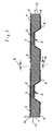
- a differential pressure sensor which is constructed of a silicon substrate 1, which is thinned out where the actual membrane of the subsequent sensor is thinned.
- This membrane area is marked with 2.
- electronic components in the form of resistors 3 are formed on the upper side as shown in FIG. 1 in the silicon substrate 1, which are connected in a conventional manner to a (not shown in detail) measuring bridge whose electrical connections in the form of Contacts 4 are led out at the top of the silicon substrate 1.
- These contacts 4 are made of aluminum, as well as the formed in the same way (not shown) interconnects to the resistors 3 and the other not described in detail here electronic components of the components.
- the silicon substrate 1 is covered with the resistors 3 formed thereon, components and the interconnects thereon, each by an insulating oxide layer, which is broken only by the contacts 4.
- the oxide layer 5 in turn is covered by a corrosion-resistant metal layer 6 in the form of a metal layer 6 formed from a chromium-tantalum alloy.
- the metal layer 6 is not only provided in the membrane region 2, but extends laterally beyond the clamping region 7 and terminates at a distance from the nearest peripheral edge 10 of the electronic component formed by the silicon substrate 1 with its formations.
- the clamping area 7 is shown in Fig. 2 by a broken line. It is apparent from the illustration of FIG. 1, in which two O-rings 8 and 9 are shown, which form the clamping in the later installation position for tightly incorporating the component into a housing. These O-rings 8, 9 then seal off the actual membrane region 2, which is protected on both sides by the metal layer 6, from the edge regions. These O-rings 8 and 9 are typically located within a sensor housing, via which the fluid is applied to both sides of the membrane 2.
- the component shown with reference to FIGS. 1 and 2 has a silicon substrate of square shape.
- the contacts 4 for the electrical connection of the component are in the corner areas.
- the metal layer 6 is circular, as shown in FIG. 2, such that the contacts 4 lie outside the circular area, wherein the diameter of the circle is chosen to be significantly smaller than the side length of the component, so that there is always a minimum distance a from the nearest outer surface. ⁇ enkante 10 of the substrate 1 is formed.
- the metal layer 6 on the underside can be square in shape according to the substrate shape, where the edge length of the square of the metal layer 6 expediently corresponds to the diameter of the circle of the metal layer 6 on the other side, in order to ensure a minimum distance a to the nearest peripheral edge 10 ,
- the above-described formation of the metal layers 6 at a distance from the peripheral edge 10 has the advantage that no special reliefs have to be created for the contacts 4, but on the other hand it is ensured that within a wafer (in FIG. 3, two components within a wafer are before severing) shown) is always ensured that the area b, in which the transection of the Wafers made to individual components, not covered by the metal layer 6.
- FIG. 3 by way of example, two components are shown as they are arranged adjacent within the wafer.
- the region marked there with b is cut out, whereby the composite of the components is separated. Since no metal layer is present in this area, the lubricating effects and impurities described at the beginning by metal parts no longer occur.
- the metal layers 6 end at a distance a from this region b, so that a certain tolerance range is formed for the kerf, which always ensures that the metal layer 6 remains unaffected during the cutting process.
- the end faces 11 formed by the cutting process are provided with a seal, which also electrically isolates and protects the substrate in this area. Since by the separation process (be it mechanically or by laser cutting) also parts of the insulating oxide layer 5 can be broken off near the peripheral edge 10, the seal is designed so that it adjoins the insulating oxide layer 5, ie beyond the peripheral edge 10 and this if necessary replaced pieces of the insulating layer 5.
Landscapes
- Physics & Mathematics (AREA)
- General Physics & Mathematics (AREA)
- Chemical & Material Sciences (AREA)
- Analytical Chemistry (AREA)
- Health & Medical Sciences (AREA)
- Child & Adolescent Psychology (AREA)
- Measuring Fluid Pressure (AREA)
- Pressure Sensors (AREA)
Abstract
Description
- Die Erfindung betrifft ein Verfahren zur Herstellung von elektronischen Bauelementen, insbesondere zur Herstellung von elektronischen Sensoren zur Druck und/oder Differenzdruckmessung gemäß den im Oberbegriff des Anspruchs 1 angegebenen Merkmalen sowie ein derartiges elektronisches Bauelement gemäß den im Oberbegriff des Anspruchs 5 angegebenen Merkmalen.
- Elektronische Bauelemente, insbesondere zum Einsatz als Druck- oder Differenzdrucksensor sind beispielsweise aus
DE 297 24 622 U1 bekannt. Sie bestehen aus einem Halbleitersubstrat, das in dem Bereich, welcher den späteren Membranbereich des Sensors bilden soll, ausgedünnt ausgebildet ist. In diesem Bereich sind auch die eigentlichen Messelemente in Form von Widerständen ausgebildet, welche typischerweise zu einer Messbrücke geschaltet sind und im späteren Einsatz aufgrund der Membrandehnung ihre Widerstandseigenschaften ändern, was wiederum als Maß für den anstehenden Druck zur elektronischen Auswertung herangezogen wird. Das Siliziumsubstrat sowie die darin ausgebildeten Messelemente sind an der Ober- bzw. Unterseite des Substrats jeweils mit einer isolierenden Schicht, typischerweise eine Oxidschicht versehen, die wiederum mit einer korrosionsfesten Metallschicht, typischerweise einer Chrom-Tantal-Schicht überzogen ist. Diese Metallschicht erstreckt sich bei bekannten Bauelementen zu beiden Seiten bis zum Rand und ist lediglich im Bereich der Anschlusskontakte unterbrochen. - Derartige elektronische Bauelemente werden nicht einzeln, sondern typischerweise in Form von Wafern hergestellt, d.h. es werden eine Vielzahl elektronischer Bauelemente nebeneinander liegend in dem Siliziumsubstrat bzw. auf dem Siliziumsubstrat ausgebildet, wonach die isolierende Schicht aufgetragen und schließlich die schützende Metallschicht aufgebracht wird. Die so gebildete Vielzahl von elektronischen Bauelementen wird dann mechanisch in einzelne Bauelemente getrennt. Dieses Verfahren wird in der Halbleitertechnik seit langem angewandt und hat sich bewährt.
- Allerdings stellt sich insbesondere bei der Herstellung von elektronischen Sensoren zur Druck- und/oder Differenzdruckmessung, welche mit einer korrosionsfesten Metallschicht versehen werden müssen, das Problem, dass beim Zerteilen des Wafers, also beim Trennen der einzelnen Bauelemente die Metallschicht randseitig nicht immer glatt abgeschnitten wird, sondern Schmiereffekte auftreten, Metallpartikel in Bereiche zwischen Anschlusskontakten und Metallschicht bzw. in den Bereich der Stirnseiten gelangen. Auch kann beim Zertrennen die isolierende Schicht im Randbereich beschädigt werden, wodurch die Metallschicht unmittelbar auf dem Substrat zur Anlage kommt und Kriechströme entstehen können. Hierdurch können die elektrischen Eigenschaften der so gebildeten Bauelemente beeinträchtigt werden. Zumindest führt dies dazu, dass die so gebildeten elektronischen Bauelemente eine vergleichsweise große Toleranz aufweisen, was nachteilig ist.
- Vor diesem Hintergrund liegt der Erfindung die Aufgabe zugrunde, ein gattungsgemäßes Verfahren so auszubilden, dass die vorgenannten Nachteile vermindert, insbesondere die dadurch möglicherweise ausgelösten Kriechströme unterbunden werden.
- Diese Aufgabe wird gemäß der Erfindung durch ein Verfahren mit den im Anspruch 1 angegebenen Merkmalen gelöst. Vorteilhafte Ausgestaltungen des erfindungsgemäßen Verfahrens sind in den Unteransprüchen angegeben.
- Ein mit dem erfindungsgemäßen Verfahren hergestelltes elektronisches Bauelement ist durch die Merkmale des Anspruchs 5 gekennzeichnet, vorteilhafte Ausgestaltungen dieses Bauelements sind durch die Merkmale der Unteransprüche 6 und 7 gekennzeichnet. Weitere vorteilhafte Ausgestaltungen der Erfindung sind in der nachfolgenden Beschreibung sowie der Zeichnung angegeben.
- Das erfindungsgemäße Verfahren sieht vor, dass zunächst auf einem Wafer die Halbleiterstrukturen der elektronischen Bauelemente erzeugt werden, wonach mindestens eine isolierende Schicht, z. B. eine Oxidschicht sowie nachfolgend mindestens eine schützende Metallschicht aufgebracht wird. Gemäß der Erfindung wird die Metallschicht jedoch abschnittsweise und nur in den Bereichen des Wafers aufgebracht, in denen später keine Teilung des Wafers mehr erfolgt. Statt die Metallschicht abschnittsweise aufzutragen kann diese alternativ vollflächig auf den Wafer, beispielsweise durch Aufdampfen aufgetragen werden, wobei danach zumindest in den Bereichen, in denen später die Zerteilung des Wafers erfolgt, die Metallschicht vor der Zerteilung entfernt wird. Bei beiden Verfahren ist also stets sichergestellt, dass vor dem Zerteilen des Wafers in den Bereichen der späteren Trennfugen keine Metallschicht vorhanden ist. Danach werden die so gebildeten elektronischen Bauelemente durch Schneiden des Wafers aus dem Verbund gelöst.
- Grundgedanke der vorliegenden Erfindung ist es also, in den Bereichen, in welchen der Wafer zur Bildung der einzelnen elektronischen Bauelemente nach dem erfolgten Fertigungsprozess zerteilt wird, nicht mit einer Metallschicht zu versehen bzw. dort die Metallschicht gezielt zu entfernen, so dass beim späteren Durchtrennen des Wafers auch keine Metallschicht durchtrennt werden muss. Das hat den Vorteil, dass die Metallschicht nicht zerteilt werden muss und damit auch nicht die eingangs geschilderten nachteiligen Effekte auftreten, welche zu einer vergleichsweisen großen Toleranz der elektrischen Eigenschaften der so gebildeten elektronischen Bauelemente führen. Das erfindungsgemäße Verfahren ermöglicht also durch das gezielte Aufbringen der Metallschicht nur in den Bereichen, in denen später keine Teilung des Wafers mehr erfolgt, die Toleranz der elektrischen Eigenschaften der so gebildeten Bauelemente erheblich zu verringern und somit die Qualität der Bauelemente zu erhöhen, ohne den Fertigungsprozess merklich zu verteuern oder aufwendiger zu gestalten, da die Metallschicht ohnehin nicht deckend, sondern stets abschnittsweise vorgesehen werden muss, da beispielsweise im Bereich der elektrischen Kontakte ohnehin auch schon bisher eine Aussparung vorgesehen sein musste.
- Fertigungstechnisch günstig ist es, den Wafer vollflächig durch Aufdampfen mit einer Metallschicht zu versehen und dann diese abschnittsweise durch chemischen oder elektrochemischen Prozess, vorteilhaft durch Ätzen zu entfernen. Das abschnittsweise Entfernen der Metallschicht kann alternativ auch durch geeignete thermische Einwirkung, beispielsweise durch Laserstrahlung erfolgen.
- Es kann jedoch auch vorteilhaft sein, die Metallschicht von vornherein abschnittsweise aufzudampfen, dann werden vorteilhaft vor dem Aufbringen der Metallschicht durch Maskierung die Bereiche abgedeckt, in denen die spätere Zerteilung des Wafers erfolgt. Die Maskierung sorgt dafür, dass die Metallschicht nicht haftet, so dass in den maskierten Bereichen keine Metallschicht aufgebracht wird.
- Wenn die Metallschicht mit ausreichendem Abstand zur späteren Trennfuge bzw. zu der dort dann umfangsseitig gebildeten Stirnseite endet, dann kann grundsätzlich eine weitere Bearbeitung dieser durch das Trennen gebildeten schmalen Stirnseiten entfallen. Wenn aber, beispielsweise aus Platzgründen der verbleibende Abstand der Metallschicht zur Trennfuge vergleichsweise gering ist, dann kann es insbesondere von Vorteil sein, wenn nach dem Zerteilen des Wafers die durch das Zerteilen gebildeten Stirnseiten versiegelt werden, beispielsweise durch eine aushärtende beim Aufbringen flüssige Versiegelung, welche elektrisch isolierende Wirkung hat. Diese Versiegelung schützt nicht nur die schmalen durch das Trennen gebildeten Stirnseiten des jeweiligen Bauelementes, sondern sorgt dafür, dass etwaige Beschädigungen, insbesondere mikroskopische Ausbrüche im Randbereich der isolierenden Schicht ausgefüllt werden, so dass sich auch in diesem Bereich keine merklichen Kriechströme ausbilden können.
- Das so gebildete elektronische Bauelement gemäß der Erfindung ist dadurch gekennzeichnet, dass seine zumindest zu einer Seite bestehende schützende Metallschicht allseits mit Abstand zu der nächstliegenden Umfangskante endet. Es versteht sich, dass der Abstand zur nächstliegenden Umfangskante einerseits so gering gewählt wird, dass in jedem Fall sichergestellt ist, dass der zu schützende Bereich, bei einem Differenzdruck- oder Drucksensor ist dies typischerweise der Membranbereich sowie der diesem umgebende Einspannbereich, durch die Metallschicht geschützt ist, andererseits so groß ist, dass sichergestellt ist, dass der spätere Trennvorgang außerhalb der Metallschicht erfolgt.
- Bei einem Differenzdrucksensor, bei welchem die durch Ausdünnung des Siliziumsubstrats gebildete Membran beidseitig druckbeaufschlagt ist, ist auch zu beiden Seiten eine schützende Metallschicht vorgesehen, welche nicht nur die Membran selbst, sondern auch den unmittelbar benachbarten Bereich, vorteilhaft über die Einspannstelle hinausgehend umfasst, damit das Bauelement zuverlässig gegen Einflüsse von Außen geschützt ist. Einspannstelle im vorgenannten Sinn ist nicht zwingend die Stelle, an welcher das Bauelement mechanisch gehalten ist, sondern die Stelle, an welcher das Bauelement gegenüber dem Medium, dessen Druck bzw. Differenzdruck zu messen ist, abgedichtet ist.
- Besonders vorteilhaft ist es, wenn das erfindungsgemäße elektronische Bauelement an seinen Stirnseiten, d. h. an den durch Trennen aus dem Wafer gebildeten Seiten mit einer Versiegelung versehen ist. Eine solche Versiegelung ist zweckmäßig so ausgelegt, dass sie in flüssiger Form aufgetragen werden kann und nach Aushärtung/Trocknung eine elektrisch isolierende sowie ggf. das Substrat gegen äußere Einflüsse schützende Schicht bildet.
- Die Erfindung beschränkt sich nicht auf ein Verfahren zur. Herstellung von Druck- oder Differenzdrucksensoren, sondern kann auch bei anderen elektronischen Bauelementen Anwendung finden, bei welchen der eingangs beschriebene nachteilige Effekt auftritt, wenn der Wafer in Einzelbauelemente getrennt wird. Es versteht sich, dass dieses Verfahren auch für solche ggf. nicht aus Metall bestehende Schichten angewendet werden kann, bei denen sich ein ähnlicher Effekt beim späteren Zerteilen einstellt.
- Die Erfindung ist nachfolgend anhand eines in der Zeichnung dargestellten Ausführungsbeispiels näher erläutert. Es zeigen:
- Fig. 1
- in stark vereinfachter schematischer Schnittdarstellung ein elektronisches Bauelement in Form eines Differenzdrucksensors mit Einspannung,
- Fig. 2
- eine Draufsicht auf ein elektronisches Bauelement gemäß Fig. 1 und
- Fig. 3
- einen Schnitt durch einen Abschnitt eines Wafers im Bereich von zwei nebeneinander liegenden elektronischen Bauelementen.
- Bei dem dargestellten elektronischen Bauelement handelt es sich um einen Differenzdrucksensor, der aus einen Siliziumsubstrat 1 aufgebaut ist, das dort, wo die eigentliche Membran des späteren Sensors entsteht, ausgedünnt ist. Dieser Membranbereich ist mit 2 gekennzeichnet. In diesem Membranbereich 2 sind an der Oberseite gemäß Darstellung nach Fig. 1 im Siliziumsubstrat 1 elektronische Bauteile in Form von Widerständen 3 ausgebildet, die in an sich bekannter Weise zu einer (nicht im Einzelnen dargestellten) Messbrücke verschaltet sind, deren elektrische Anschlüsse in Form von Kontakten 4 an der Oberseite des Siliziumsubstrats 1 herausgeführt sind. Diese Kontakte 4 bestehen aus Aluminium, ebenso wie die in gleicher Weise gebildeten (nicht dargestellten) Leiterbahnen zu den Widerständen 3 sowie den weiteren hier nicht im Einzelnen beschriebenen elektronischen Bauteilen der Bauelemente.
- Beidseitig ist das Siliziumsubstrat 1 mit den darin ausgebildeten Widerständen 3, Bauteilen sowie den darauf befindlichen Leiterbahnen durch je eine isolierende Oxidschicht abgedeckt, die lediglich durch die Kontakte 4 durchbrochen wird.
- Die Oxidschicht 5 wiederum ist durch eine korrosionsbeständige Metallschicht 6 in Form einer aus einer Chrom-Tantal-Legierung gebildeten Metallschicht 6 abgedeckt. Die Metallschicht 6 ist nicht nur im Membranbereich 2 vorgesehen, sondern reicht seitlich über den Einspannbereich 7 hinaus und endet mit Abstand zu der nächstliegenden Umfangskante 10 des durch das Siliziumsubstrat 1 mit seinen Ausbildungen gebildeten elektronischen Bauelementes. Der Einspannbereich 7 ist in Fig. 2 durch eine unterbrochene Linie dargestellt. Er ergibt sich aus der Darstellung nach Fig. 1, in welcher zwei O-Ringe 8 und 9 dargestellt sind, welche in der späteren Einbaulage die Einspannung zum dichten Eingliedern des Bauelements in ein Gehäuse bilden. Diese O-Ringe 8, 9 dichten dann den eigentlichen Membranbereich 2, welcher durch die Metallschicht 6 beidseitig geschützt ist, gegenüber den Randbereichen ab. Diese O-Ringe 8 und 9 liegen typischerweise innerhalb eines Sensorgehäuses, über welches die Fluidbeaufschlagung zu beiden Seiten der Membran 2 erfolgt.
- Das anhand der Figuren 1 und 2 dargestellte Bauelement weist ein Siliziumsubstrat quadratischer Form auf. Die Kontakte 4 zum elektrischen Anschluss des Bauelementes liegen in den Eckbereichen. Die Metallschicht 6 ist, wie Fig. 2 zeigt, kreisförmig ausgebildet, derart, dass die Kontakte 4 außerhalb der Kreisfläche liegen, wobei der Durchmesser des Kreises deutlich kleiner als die Seitenlänge des Bauelements gewählt ist, so dass stets ein Mindestabstand a zur nächstliegenden Au-βenkante 10 des Substrates 1 gebildet ist. Die Metallschicht 6 an der Unterseite kann hingegen quadratisch entsprechend der Substratform ausgebildet sein, wobei dort die Kantenlänge des Quadrates der Metallschicht 6 zweckmäßigerweise dem Durchmesser des Kreises der Metallschicht 6 auf der anderen Seite entspricht, um auch hier einen Mindestabstand a zur nächstliegenden Umfangskante 10 zu gewährleisten.
- Die vorbeschriebene Ausbildung der Metallschichten 6 mit Abstand zur Umfangskante 10 hat den Vorteil, dass für die Kontakte 4 keine besonderen Freistellen geschaffen werden müssen, andererseits jedoch sichergestellt ist, dass innerhalb eines Wafers (in Fig. 3 sind zwei Bauelemente innerhalb eines Wafers vor dem Durchtrennen dargestellt) stets sichergestellt ist, dass der Bereich b, in welchem die Durchtrennung des Wafers zu einzelnen Bauelementen erfolgt, nicht von der Metallschicht 6 bedeckt ist.
- In Fig. 3 sind beispielhaft zwei Bauelemente so dargestellt, wie sie innerhalb des Wafers benachbart angeordnet sind. Beim Durchtrennen des Wafers nach Abschluss des eigentlichen Fertigungsprozesses der Bauelemente wird der dort mit b gekennzeichnete Bereich herausgetrennt, wodurch der Verbund der Bauelemente getrennt wird. Da in diesem Bereich keine Metallschicht vorhanden ist, treten die eingangs beschriebenen Schmiereffekte und Verunreinigungen durch Metallteile nicht mehr auf. Wie die Fig. 3 deutlich zeigt, enden die Metallschichten 6 mit einem Abstand a zu diesem Bereich b, so dass für die Schnittfuge ein gewisser Toleranzbereich gebildet ist, der stets sicherstellt, dass beim Schneidvorgang die Metallschicht 6 unberührt bleibt.
- Die durch den Schneidvorgang gebildeten Stirnseiten 11 sind mit einer Versiegelung versehen, die das Substrat auch in diesem Bereich elektrisch isoliert und schützt. Da durch den Trennvorgang (sei es mechanisch oder durch Laserschneiden) nahe der Umfangskante 10 auch Teile der isolierenden Oxidschicht 5 herausgebrochen werden können, ist die Versiegelung so ausgelegt, dass sie an die isolierende Oxidschicht 5 anschließt, d. h. über die Umfangskante 10 hinausgeht und diese ggf. herausgebrochenen Teile der isolierenden Schicht 5 ersetzt.
-
- 1
- Siliziumsubstrat
- 2
- Membranbereich
- 3
- Widerstände
- 4
- Kontakte
- 5
- Isolierende Oxidschicht
- 6
- Metallschicht
- 7
- Einspannbereich
- 8
- O-Ring oben
- 9
- O-Ring unten
- 10
- Umfangskante
- 11
- Stirnseiten
- a
- Mindestabstand
- b
- Bereich der Trennstelle des Wafers
Claims (7)
- Verfahren zur Herstellung von elektronischen Bauelementen, insbesondere zur Herstellung von elektronischen Sensoren zur Druck- und/oder Differenzdruckmessung, bei dem zunächst auf einem Wafer die Halbleiterstrukturen der elektronischen Bauelemente (3) erzeugt werden, wonach mindestens eine isolierende Schicht (5) sowie nachfolgend mindestens eine schützende Metallschicht (6) aufgebracht wird, wonach der Wafer in die so gebildeten elektronischen Bauelemente (3), insbesondere Sensoren zerteilt wird, dadurch gekennzeichnet, dass die Metallschicht (6) entweder abschnittweise und nur in den Bereichen des Wafers aufgebracht wird, in denen später keine Zerteilung des Wafers mehr erfolgt, oder dass zumindest in den Bereichen, in denen später die Zerteilung des Wafers erfolgt, die Metallschicht vor der Zerteilung entfernt wird.
- Verfahren nach Anspruch 1, dadurch gekennzeichnet, dass das abschnittsweise Entfernen der Metallschicht durch Ätzen oder durch Einwirkung von Laserstrahlung erfolgt.
- Verfahren nach Anspruch 1, dadurch gekennzeichnet, dass vor dem Aufbringen der Metallschicht durch Maskierung mindestens die Bereiche abgedeckt werden, in denen die spätere Zerteilung des Wafers erfolgt.
- Verfahren nach einem der vorhergehenden Ansprüche, dadurch gekennzeichnet, dass nach dem Zerteilen des Wafers die durch das Zerteilen gebildeten Stirnseiten 11 versiegelt werden.
- Elektronisches Bauelement in Form eines Druck- oder Differenzdrucksensor, das durch Trennen aus einem Wafer gebildet ist, und das mindestens eine schützende Metallschicht (6) aufweist, dadurch gekennzeichnet, dass die Metallschicht (6) allseits mit Abstand (a) zu der nächstliegenden Umfangskante (10) endet.
- Elektronisches Bauelement nach Anspruch 5, dadurch gekennzeichnet, dass das Bauelement einen zumindest einseitig ausgedünnten Bereich (2) aufweist, in welchem die den Sensor bildenden Halbleiterstrukturen (3) gebildet sind und dass beide Seiten dieses ausgedünnten Bereichs (2) mit einer schützenden Metallschicht (6) versehen sind, wobei beide Metallschichten (6) allseits mit Abstand (a) zur jeweils nächstliegenden Umfangskante (10) enden.
- Elektronisches Bauelement nach Anspruch 5 oder 6, dadurch gekennzeichnet, dass die Stirnseiten 11 mit einer Versiegelung versehen sind.
Priority Applications (6)
| Application Number | Priority Date | Filing Date | Title |
|---|---|---|---|
| EP06002983A EP1821091B1 (de) | 2006-02-15 | 2006-02-15 | Verfahren zur Herstellung von elektronischen Bauelementen und Drucksensor |
| DE502006009096T DE502006009096D1 (de) | 2006-02-15 | 2006-02-15 | Verfahren zur Herstellung von elektronischen Bauelementen und Drucksensor |
| AT06002983T ATE502289T1 (de) | 2006-02-15 | 2006-02-15 | Verfahren zur herstellung von elektronischen bauelementen und drucksensor |
| CN2007800057101A CN101389941B (zh) | 2006-02-15 | 2007-01-30 | 压力或压差传感器及电子传感器的制造方法 |
| US12/279,370 US8026121B2 (en) | 2006-02-15 | 2007-01-30 | Method for producing electronic components and pressure sensor |
| PCT/EP2007/000780 WO2007093279A2 (de) | 2006-02-15 | 2007-01-30 | Verfahren zur herstellung von elektronischen bauelementen und drucksensor |
Applications Claiming Priority (1)
| Application Number | Priority Date | Filing Date | Title |
|---|---|---|---|
| EP06002983A EP1821091B1 (de) | 2006-02-15 | 2006-02-15 | Verfahren zur Herstellung von elektronischen Bauelementen und Drucksensor |
Publications (2)
| Publication Number | Publication Date |
|---|---|
| EP1821091A1 true EP1821091A1 (de) | 2007-08-22 |
| EP1821091B1 EP1821091B1 (de) | 2011-03-16 |
Family
ID=36616819
Family Applications (1)
| Application Number | Title | Priority Date | Filing Date |
|---|---|---|---|
| EP06002983A Expired - Lifetime EP1821091B1 (de) | 2006-02-15 | 2006-02-15 | Verfahren zur Herstellung von elektronischen Bauelementen und Drucksensor |
Country Status (6)
| Country | Link |
|---|---|
| US (1) | US8026121B2 (de) |
| EP (1) | EP1821091B1 (de) |
| CN (1) | CN101389941B (de) |
| AT (1) | ATE502289T1 (de) |
| DE (1) | DE502006009096D1 (de) |
| WO (1) | WO2007093279A2 (de) |
Families Citing this family (4)
| Publication number | Priority date | Publication date | Assignee | Title |
|---|---|---|---|---|
| US9310267B2 (en) | 2014-02-28 | 2016-04-12 | Measurement Specialities, Inc. | Differential pressure sensor |
| US9316552B2 (en) | 2014-02-28 | 2016-04-19 | Measurement Specialties, Inc. | Differential pressure sensing die |
| US9593995B2 (en) | 2014-02-28 | 2017-03-14 | Measurement Specialties, Inc. | Package for a differential pressure sensing die |
| CN114112168B (zh) * | 2021-12-01 | 2024-11-19 | 上海文襄汽车传感器有限公司 | 一种陶瓷电容压力传感器及其制造方法 |
Citations (2)
| Publication number | Priority date | Publication date | Assignee | Title |
|---|---|---|---|---|
| DE4415984A1 (de) | 1994-05-06 | 1995-11-09 | Bosch Gmbh Robert | Halbleitersensor mit Schutzschicht |
| DE29724622U1 (de) | 1996-04-12 | 2002-07-25 | Grundfos A/S, Bjerringbro | Elektronisches Bauelement |
Family Cites Families (8)
| Publication number | Priority date | Publication date | Assignee | Title |
|---|---|---|---|---|
| US4115120A (en) * | 1977-09-29 | 1978-09-19 | International Business Machines Corporation | Method of forming thin film patterns by differential pre-baking of resist |
| US5521125A (en) * | 1994-10-28 | 1996-05-28 | Xerox Corporation | Precision dicing of silicon chips from a wafer |
| DE29724662U1 (de) | 1996-02-05 | 2002-08-01 | E.G.O. Elektro-Gerätebau Gmbh, 75038 Oberderdingen | Sensor zur Kochgefässerkennung |
| DE19614459A1 (de) * | 1996-04-12 | 1997-10-16 | Grundfos As | Elektronisches Bauelement |
| US5904548A (en) * | 1996-11-21 | 1999-05-18 | Texas Instruments Incorporated | Trench scribe line for decreased chip spacing |
| US6303977B1 (en) * | 1998-12-03 | 2001-10-16 | Texas Instruments Incorporated | Fully hermetic semiconductor chip, including sealed edge sides |
| JP2002190607A (ja) * | 2000-12-22 | 2002-07-05 | Denso Corp | 半導体装置及びその製造方法 |
| US7713771B2 (en) * | 2006-09-01 | 2010-05-11 | Grundfos A/S | Pressure sensor |
-
2006
- 2006-02-15 AT AT06002983T patent/ATE502289T1/de active
- 2006-02-15 EP EP06002983A patent/EP1821091B1/de not_active Expired - Lifetime
- 2006-02-15 DE DE502006009096T patent/DE502006009096D1/de not_active Expired - Lifetime
-
2007
- 2007-01-30 CN CN2007800057101A patent/CN101389941B/zh not_active Expired - Fee Related
- 2007-01-30 US US12/279,370 patent/US8026121B2/en not_active Expired - Fee Related
- 2007-01-30 WO PCT/EP2007/000780 patent/WO2007093279A2/de not_active Ceased
Patent Citations (2)
| Publication number | Priority date | Publication date | Assignee | Title |
|---|---|---|---|---|
| DE4415984A1 (de) | 1994-05-06 | 1995-11-09 | Bosch Gmbh Robert | Halbleitersensor mit Schutzschicht |
| DE29724622U1 (de) | 1996-04-12 | 2002-07-25 | Grundfos A/S, Bjerringbro | Elektronisches Bauelement |
Also Published As
| Publication number | Publication date |
|---|---|
| US8026121B2 (en) | 2011-09-27 |
| WO2007093279A2 (de) | 2007-08-23 |
| US20090004766A1 (en) | 2009-01-01 |
| WO2007093279A3 (de) | 2008-02-14 |
| DE502006009096D1 (de) | 2011-04-28 |
| ATE502289T1 (de) | 2011-04-15 |
| CN101389941A (zh) | 2009-03-18 |
| CN101389941B (zh) | 2011-07-06 |
| EP1821091B1 (de) | 2011-03-16 |
Similar Documents
| Publication | Publication Date | Title |
|---|---|---|
| DE3134343C2 (de) | Halbleiteranordnung | |
| DE68926652T2 (de) | Halbleiterpackung ohne Montierungsfläche | |
| DE10325020B4 (de) | Verfahren zum Versiegeln eines Halbleiterbauelements und damit hergestellte Vorrichtung | |
| DE102013222517A1 (de) | Mikromechanische Sensoreinheit und Verfahren zur Herstellung von mikromechanischen Sensoreinheiten | |
| EP2737497B1 (de) | Verfahren zum herstellen eines elektrischen bauelements und elektrisches bauelement | |
| DE102012215524A1 (de) | Optoelektronisches Halbleiterbauteil | |
| DE102004028927B4 (de) | Beschleunigungssensor | |
| WO2007087912A1 (de) | Verfahren zum elektrischen kontaktieren eines elektronischen bauelements | |
| DE102011076883B4 (de) | Halbleitervorrichtungen | |
| WO2007093279A2 (de) | Verfahren zur herstellung von elektronischen bauelementen und drucksensor | |
| DE102014217271A1 (de) | Verfahren zur Herstellung einer Halbleitervorrichtung | |
| DE102013204014B4 (de) | Steuergerät für ein Kraftfahrzeug und Verfahren zur Herstellung eines Steuergerätes | |
| DE4417670A1 (de) | Verbessertes TAB-Band | |
| EP4045882B1 (de) | Sensorelement und verfahren zur herstellung eines sensorelements | |
| WO2017144691A1 (de) | Optoelektronisches bauteil mit einem leiterrahmenabschnitt | |
| DE102005003390B4 (de) | Substrat für ein FBGA-Halbleiterbauelement | |
| DE102015114579B4 (de) | Halbleiterchip | |
| DE19736754A1 (de) | Überspannungsschutzelement | |
| DE19845537A1 (de) | Sensor und Verfahren zu seiner Herstellung | |
| EP1111671B1 (de) | Verfahren zum Herstellen einer Halbleiteranordnung | |
| EP2260511B1 (de) | Bauelementanordnung und verfahren zur herstellung einer bauelementanordnung | |
| DE10104265A1 (de) | Verfahren zum Herstellen einer Halbleiterschaltungsanordnung | |
| DE102014217938B4 (de) | Elektronisches Bauelement | |
| DE102019220215A1 (de) | Verfahren zur Herstellung von Halbleiterbauelementen und Halbleiterbauelement | |
| EP2463900A2 (de) | Verfahren zur Herstellung einer Schaltungsanordnung |
Legal Events
| Date | Code | Title | Description |
|---|---|---|---|
| PUAI | Public reference made under article 153(3) epc to a published international application that has entered the european phase |
Free format text: ORIGINAL CODE: 0009012 |
|
| AK | Designated contracting states |
Kind code of ref document: A1 Designated state(s): AT BE BG CH CY CZ DE DK EE ES FI FR GB GR HU IE IS IT LI LT LU LV MC NL PL PT RO SE SI SK TR |
|
| AX | Request for extension of the european patent |
Extension state: AL BA HR MK YU |
|
| 17P | Request for examination filed |
Effective date: 20071127 |
|
| 17Q | First examination report despatched |
Effective date: 20080319 |
|
| AKX | Designation fees paid |
Designated state(s): AT BE BG CH CY CZ DE DK EE ES FI FR GB GR HU IE IS IT LI LT LU LV MC NL PL PT RO SE SI SK TR |
|
| GRAP | Despatch of communication of intention to grant a patent |
Free format text: ORIGINAL CODE: EPIDOSNIGR1 |
|
| GRAS | Grant fee paid |
Free format text: ORIGINAL CODE: EPIDOSNIGR3 |
|
| GRAA | (expected) grant |
Free format text: ORIGINAL CODE: 0009210 |
|
| AK | Designated contracting states |
Kind code of ref document: B1 Designated state(s): AT BE BG CH CY CZ DE DK EE ES FI FR GB GR HU IE IS IT LI LT LU LV MC NL PL PT RO SE SI SK TR |
|
| REG | Reference to a national code |
Ref country code: GB Ref legal event code: FG4D Free format text: NOT ENGLISH |
|
| REG | Reference to a national code |
Ref country code: CH Ref legal event code: EP |
|
| REG | Reference to a national code |
Ref country code: IE Ref legal event code: FG4D |
|
| REF | Corresponds to: |
Ref document number: 502006009096 Country of ref document: DE Date of ref document: 20110428 Kind code of ref document: P |
|
| REG | Reference to a national code |
Ref country code: DE Ref legal event code: R096 Ref document number: 502006009096 Country of ref document: DE Effective date: 20110428 |
|
| REG | Reference to a national code |
Ref country code: NL Ref legal event code: VDEP Effective date: 20110316 |
|
| PG25 | Lapsed in a contracting state [announced via postgrant information from national office to epo] |
Ref country code: LT Free format text: LAPSE BECAUSE OF FAILURE TO SUBMIT A TRANSLATION OF THE DESCRIPTION OR TO PAY THE FEE WITHIN THE PRESCRIBED TIME-LIMIT Effective date: 20110316 Ref country code: GR Free format text: LAPSE BECAUSE OF FAILURE TO SUBMIT A TRANSLATION OF THE DESCRIPTION OR TO PAY THE FEE WITHIN THE PRESCRIBED TIME-LIMIT Effective date: 20110617 Ref country code: ES Free format text: LAPSE BECAUSE OF FAILURE TO SUBMIT A TRANSLATION OF THE DESCRIPTION OR TO PAY THE FEE WITHIN THE PRESCRIBED TIME-LIMIT Effective date: 20110627 Ref country code: LV Free format text: LAPSE BECAUSE OF FAILURE TO SUBMIT A TRANSLATION OF THE DESCRIPTION OR TO PAY THE FEE WITHIN THE PRESCRIBED TIME-LIMIT Effective date: 20110316 Ref country code: SE Free format text: LAPSE BECAUSE OF FAILURE TO SUBMIT A TRANSLATION OF THE DESCRIPTION OR TO PAY THE FEE WITHIN THE PRESCRIBED TIME-LIMIT Effective date: 20110316 |
|
| LTIE | Lt: invalidation of european patent or patent extension |
Effective date: 20110316 |
|
| PG25 | Lapsed in a contracting state [announced via postgrant information from national office to epo] |
Ref country code: FI Free format text: LAPSE BECAUSE OF FAILURE TO SUBMIT A TRANSLATION OF THE DESCRIPTION OR TO PAY THE FEE WITHIN THE PRESCRIBED TIME-LIMIT Effective date: 20110316 Ref country code: SI Free format text: LAPSE BECAUSE OF FAILURE TO SUBMIT A TRANSLATION OF THE DESCRIPTION OR TO PAY THE FEE WITHIN THE PRESCRIBED TIME-LIMIT Effective date: 20110316 Ref country code: CY Free format text: LAPSE BECAUSE OF FAILURE TO SUBMIT A TRANSLATION OF THE DESCRIPTION OR TO PAY THE FEE WITHIN THE PRESCRIBED TIME-LIMIT Effective date: 20110316 Ref country code: BG Free format text: LAPSE BECAUSE OF FAILURE TO SUBMIT A TRANSLATION OF THE DESCRIPTION OR TO PAY THE FEE WITHIN THE PRESCRIBED TIME-LIMIT Effective date: 20110616 |
|
| REG | Reference to a national code |
Ref country code: IE Ref legal event code: FD4D |
|
| PG25 | Lapsed in a contracting state [announced via postgrant information from national office to epo] |
Ref country code: EE Free format text: LAPSE BECAUSE OF FAILURE TO SUBMIT A TRANSLATION OF THE DESCRIPTION OR TO PAY THE FEE WITHIN THE PRESCRIBED TIME-LIMIT Effective date: 20110316 Ref country code: IE Free format text: LAPSE BECAUSE OF FAILURE TO SUBMIT A TRANSLATION OF THE DESCRIPTION OR TO PAY THE FEE WITHIN THE PRESCRIBED TIME-LIMIT Effective date: 20110316 Ref country code: PT Free format text: LAPSE BECAUSE OF FAILURE TO SUBMIT A TRANSLATION OF THE DESCRIPTION OR TO PAY THE FEE WITHIN THE PRESCRIBED TIME-LIMIT Effective date: 20110718 |
|
| PG25 | Lapsed in a contracting state [announced via postgrant information from national office to epo] |
Ref country code: RO Free format text: LAPSE BECAUSE OF FAILURE TO SUBMIT A TRANSLATION OF THE DESCRIPTION OR TO PAY THE FEE WITHIN THE PRESCRIBED TIME-LIMIT Effective date: 20110316 Ref country code: SK Free format text: LAPSE BECAUSE OF FAILURE TO SUBMIT A TRANSLATION OF THE DESCRIPTION OR TO PAY THE FEE WITHIN THE PRESCRIBED TIME-LIMIT Effective date: 20110316 Ref country code: CZ Free format text: LAPSE BECAUSE OF FAILURE TO SUBMIT A TRANSLATION OF THE DESCRIPTION OR TO PAY THE FEE WITHIN THE PRESCRIBED TIME-LIMIT Effective date: 20110316 Ref country code: IS Free format text: LAPSE BECAUSE OF FAILURE TO SUBMIT A TRANSLATION OF THE DESCRIPTION OR TO PAY THE FEE WITHIN THE PRESCRIBED TIME-LIMIT Effective date: 20110716 |
|
| PG25 | Lapsed in a contracting state [announced via postgrant information from national office to epo] |
Ref country code: NL Free format text: LAPSE BECAUSE OF FAILURE TO SUBMIT A TRANSLATION OF THE DESCRIPTION OR TO PAY THE FEE WITHIN THE PRESCRIBED TIME-LIMIT Effective date: 20110316 |
|
| PLBE | No opposition filed within time limit |
Free format text: ORIGINAL CODE: 0009261 |
|
| STAA | Information on the status of an ep patent application or granted ep patent |
Free format text: STATUS: NO OPPOSITION FILED WITHIN TIME LIMIT |
|
| 26N | No opposition filed |
Effective date: 20111219 |
|
| PG25 | Lapsed in a contracting state [announced via postgrant information from national office to epo] |
Ref country code: DK Free format text: LAPSE BECAUSE OF FAILURE TO SUBMIT A TRANSLATION OF THE DESCRIPTION OR TO PAY THE FEE WITHIN THE PRESCRIBED TIME-LIMIT Effective date: 20110316 Ref country code: PL Free format text: LAPSE BECAUSE OF FAILURE TO SUBMIT A TRANSLATION OF THE DESCRIPTION OR TO PAY THE FEE WITHIN THE PRESCRIBED TIME-LIMIT Effective date: 20110316 |
|
| REG | Reference to a national code |
Ref country code: DE Ref legal event code: R097 Ref document number: 502006009096 Country of ref document: DE Effective date: 20111219 |
|
| BERE | Be: lapsed |
Owner name: GRUNDFOS MANAGEMENT A/S Effective date: 20120228 |
|
| PG25 | Lapsed in a contracting state [announced via postgrant information from national office to epo] |
Ref country code: MC Free format text: LAPSE BECAUSE OF NON-PAYMENT OF DUE FEES Effective date: 20120229 |
|
| REG | Reference to a national code |
Ref country code: CH Ref legal event code: PL |
|
| PG25 | Lapsed in a contracting state [announced via postgrant information from national office to epo] |
Ref country code: LI Free format text: LAPSE BECAUSE OF NON-PAYMENT OF DUE FEES Effective date: 20120229 Ref country code: CH Free format text: LAPSE BECAUSE OF NON-PAYMENT OF DUE FEES Effective date: 20120229 |
|
| PG25 | Lapsed in a contracting state [announced via postgrant information from national office to epo] |
Ref country code: BE Free format text: LAPSE BECAUSE OF NON-PAYMENT OF DUE FEES Effective date: 20120228 |
|
| REG | Reference to a national code |
Ref country code: AT Ref legal event code: MM01 Ref document number: 502289 Country of ref document: AT Kind code of ref document: T Effective date: 20120215 |
|
| PG25 | Lapsed in a contracting state [announced via postgrant information from national office to epo] |
Ref country code: AT Free format text: LAPSE BECAUSE OF NON-PAYMENT OF DUE FEES Effective date: 20120215 |
|
| PG25 | Lapsed in a contracting state [announced via postgrant information from national office to epo] |
Ref country code: TR Free format text: LAPSE BECAUSE OF FAILURE TO SUBMIT A TRANSLATION OF THE DESCRIPTION OR TO PAY THE FEE WITHIN THE PRESCRIBED TIME-LIMIT Effective date: 20110316 |
|
| PG25 | Lapsed in a contracting state [announced via postgrant information from national office to epo] |
Ref country code: LU Free format text: LAPSE BECAUSE OF NON-PAYMENT OF DUE FEES Effective date: 20120215 |
|
| PG25 | Lapsed in a contracting state [announced via postgrant information from national office to epo] |
Ref country code: HU Free format text: LAPSE BECAUSE OF FAILURE TO SUBMIT A TRANSLATION OF THE DESCRIPTION OR TO PAY THE FEE WITHIN THE PRESCRIBED TIME-LIMIT Effective date: 20060215 |
|
| REG | Reference to a national code |
Ref country code: FR Ref legal event code: PLFP Year of fee payment: 11 |
|
| REG | Reference to a national code |
Ref country code: FR Ref legal event code: PLFP Year of fee payment: 12 |
|
| REG | Reference to a national code |
Ref country code: FR Ref legal event code: PLFP Year of fee payment: 13 |
|
| PGFP | Annual fee paid to national office [announced via postgrant information from national office to epo] |
Ref country code: GB Payment date: 20220221 Year of fee payment: 17 Ref country code: DE Payment date: 20220221 Year of fee payment: 17 |
|
| PGFP | Annual fee paid to national office [announced via postgrant information from national office to epo] |
Ref country code: IT Payment date: 20220228 Year of fee payment: 17 Ref country code: FR Payment date: 20220221 Year of fee payment: 17 |
|
| REG | Reference to a national code |
Ref country code: DE Ref legal event code: R082 Ref document number: 502006009096 Country of ref document: DE |
|
| REG | Reference to a national code |
Ref country code: DE Ref legal event code: R119 Ref document number: 502006009096 Country of ref document: DE |
|
| GBPC | Gb: european patent ceased through non-payment of renewal fee |
Effective date: 20230215 |
|
| PG25 | Lapsed in a contracting state [announced via postgrant information from national office to epo] |
Ref country code: GB Free format text: LAPSE BECAUSE OF NON-PAYMENT OF DUE FEES Effective date: 20230215 |
|
| PG25 | Lapsed in a contracting state [announced via postgrant information from national office to epo] |
Ref country code: IT Free format text: LAPSE BECAUSE OF NON-PAYMENT OF DUE FEES Effective date: 20230215 Ref country code: GB Free format text: LAPSE BECAUSE OF NON-PAYMENT OF DUE FEES Effective date: 20230215 Ref country code: FR Free format text: LAPSE BECAUSE OF NON-PAYMENT OF DUE FEES Effective date: 20230228 Ref country code: DE Free format text: LAPSE BECAUSE OF NON-PAYMENT OF DUE FEES Effective date: 20230901 |