EP1816687A2 - Halbleiterbauelement und Verfahren zur Herstellung eines Halbleiterbauelements - Google Patents
Halbleiterbauelement und Verfahren zur Herstellung eines Halbleiterbauelements Download PDFInfo
- Publication number
- EP1816687A2 EP1816687A2 EP07002224A EP07002224A EP1816687A2 EP 1816687 A2 EP1816687 A2 EP 1816687A2 EP 07002224 A EP07002224 A EP 07002224A EP 07002224 A EP07002224 A EP 07002224A EP 1816687 A2 EP1816687 A2 EP 1816687A2
- Authority
- EP
- European Patent Office
- Prior art keywords
- light
- semiconductor device
- light emitting
- emitting device
- substrate
- Prior art date
- Legal status (The legal status is an assumption and is not a legal conclusion. Google has not performed a legal analysis and makes no representation as to the accuracy of the status listed.)
- Withdrawn
Links
Images


Classifications
-
- H—ELECTRICITY
- H01—ELECTRIC ELEMENTS
- H01L—SEMICONDUCTOR DEVICES NOT COVERED BY CLASS H10
- H01L33/00—Semiconductor devices with at least one potential-jump barrier or surface barrier specially adapted for light emission; Processes or apparatus specially adapted for the manufacture or treatment thereof or of parts thereof; Details thereof
- H01L33/48—Semiconductor devices with at least one potential-jump barrier or surface barrier specially adapted for light emission; Processes or apparatus specially adapted for the manufacture or treatment thereof or of parts thereof; Details thereof characterised by the semiconductor body packages
- H01L33/58—Optical field-shaping elements
-
- H—ELECTRICITY
- H01—ELECTRIC ELEMENTS
- H01L—SEMICONDUCTOR DEVICES NOT COVERED BY CLASS H10
- H01L24/00—Arrangements for connecting or disconnecting semiconductor or solid-state bodies; Methods or apparatus related thereto
- H01L24/93—Batch processes
- H01L24/95—Batch processes at chip-level, i.e. with connecting carried out on a plurality of singulated devices, i.e. on diced chips
- H01L24/97—Batch processes at chip-level, i.e. with connecting carried out on a plurality of singulated devices, i.e. on diced chips the devices being connected to a common substrate, e.g. interposer, said common substrate being separable into individual assemblies after connecting
-
- H—ELECTRICITY
- H01—ELECTRIC ELEMENTS
- H01L—SEMICONDUCTOR DEVICES NOT COVERED BY CLASS H10
- H01L2224/00—Indexing scheme for arrangements for connecting or disconnecting semiconductor or solid-state bodies and methods related thereto as covered by H01L24/00
- H01L2224/01—Means for bonding being attached to, or being formed on, the surface to be connected, e.g. chip-to-package, die-attach, "first-level" interconnects; Manufacturing methods related thereto
- H01L2224/10—Bump connectors; Manufacturing methods related thereto
- H01L2224/12—Structure, shape, material or disposition of the bump connectors prior to the connecting process
- H01L2224/13—Structure, shape, material or disposition of the bump connectors prior to the connecting process of an individual bump connector
-
- H—ELECTRICITY
- H01—ELECTRIC ELEMENTS
- H01L—SEMICONDUCTOR DEVICES NOT COVERED BY CLASS H10
- H01L2224/00—Indexing scheme for arrangements for connecting or disconnecting semiconductor or solid-state bodies and methods related thereto as covered by H01L24/00
- H01L2224/01—Means for bonding being attached to, or being formed on, the surface to be connected, e.g. chip-to-package, die-attach, "first-level" interconnects; Manufacturing methods related thereto
- H01L2224/42—Wire connectors; Manufacturing methods related thereto
- H01L2224/47—Structure, shape, material or disposition of the wire connectors after the connecting process
- H01L2224/48—Structure, shape, material or disposition of the wire connectors after the connecting process of an individual wire connector
- H01L2224/4805—Shape
- H01L2224/4809—Loop shape
- H01L2224/48091—Arched
-
- H—ELECTRICITY
- H01—ELECTRIC ELEMENTS
- H01L—SEMICONDUCTOR DEVICES NOT COVERED BY CLASS H10
- H01L2924/00—Indexing scheme for arrangements or methods for connecting or disconnecting semiconductor or solid-state bodies as covered by H01L24/00
- H01L2924/10—Details of semiconductor or other solid state devices to be connected
- H01L2924/11—Device type
- H01L2924/12—Passive devices, e.g. 2 terminal devices
- H01L2924/1204—Optical Diode
- H01L2924/12041—LED
-
- H—ELECTRICITY
- H01—ELECTRIC ELEMENTS
- H01L—SEMICONDUCTOR DEVICES NOT COVERED BY CLASS H10
- H01L33/00—Semiconductor devices with at least one potential-jump barrier or surface barrier specially adapted for light emission; Processes or apparatus specially adapted for the manufacture or treatment thereof or of parts thereof; Details thereof
- H01L33/44—Semiconductor devices with at least one potential-jump barrier or surface barrier specially adapted for light emission; Processes or apparatus specially adapted for the manufacture or treatment thereof or of parts thereof; Details thereof characterised by the coatings, e.g. passivation layer or anti-reflective coating
-
- H—ELECTRICITY
- H01—ELECTRIC ELEMENTS
- H01L—SEMICONDUCTOR DEVICES NOT COVERED BY CLASS H10
- H01L33/00—Semiconductor devices with at least one potential-jump barrier or surface barrier specially adapted for light emission; Processes or apparatus specially adapted for the manufacture or treatment thereof or of parts thereof; Details thereof
- H01L33/48—Semiconductor devices with at least one potential-jump barrier or surface barrier specially adapted for light emission; Processes or apparatus specially adapted for the manufacture or treatment thereof or of parts thereof; Details thereof characterised by the semiconductor body packages
- H01L33/50—Wavelength conversion elements
- H01L33/507—Wavelength conversion elements the elements being in intimate contact with parts other than the semiconductor body or integrated with parts other than the semiconductor body
-
- H—ELECTRICITY
- H01—ELECTRIC ELEMENTS
- H01L—SEMICONDUCTOR DEVICES NOT COVERED BY CLASS H10
- H01L33/00—Semiconductor devices with at least one potential-jump barrier or surface barrier specially adapted for light emission; Processes or apparatus specially adapted for the manufacture or treatment thereof or of parts thereof; Details thereof
- H01L33/48—Semiconductor devices with at least one potential-jump barrier or surface barrier specially adapted for light emission; Processes or apparatus specially adapted for the manufacture or treatment thereof or of parts thereof; Details thereof characterised by the semiconductor body packages
- H01L33/58—Optical field-shaping elements
- H01L33/60—Reflective elements
Definitions
- the present disclosure relates to a semiconductor device and a method of manufacturing the semiconductor device, and more particularly to a semiconductor device in which an optical functional device such as a light emitting device or a light receiving device is mounted on a substrate and a method of manufacturing the semiconductor device.
- a type of a luminescent color thereof is limited.
- a phosphor for emitting a light corresponding to a light emission of the LED is used and a compound color of a light emission of the LED and that of a phosphor is utilized in some cases.
- a related-art semiconductor device in which a light emitting device is mounted have such a structure that a light emitting device is mounted in a concave portion of a substrate and an upper opening of the concave portion is sealed with an optical member (glass) such as a glass, and a fluorescent member formed on a lower surface of the optical member emits a light upon receipt of a light emitted from the light emitting device, thereby increasing an intensity of a light emitted from the optical member (for example, see Japanese Patent Unexamined Publication No. 2003-110146 ).
- the total reflection of the light implies a phenomenon generated when the light proceeds from a medium having a high refractive index to a medium having a low refractive index.
- the phenomenon might be generated.
- the light emitting device has a structure in which the light is irradiated toward an upper surface of the light emitting device, the light subjected to the total reflection in the inner part of the light emitting device is irradiated from a side surface of the light emitting device. For this reason, there is also a problem in that an intensity of the light emitted from the upper surface of the light emitting device as an original light emitting surface is reduced.
- the semiconductor device according to independent claim 1 and the method of manufacturing a semiconductor device according to independent claim 6 are provided.
- Embodiments of the present invention provide a semiconductor device.
- One or more embodiments of the invention have the following means.
- One or more embodiments of the invention provides a semiconductor device in which an optical functional device is mounted on a substrate, wherein a cover having a light transparency is disposed above the optical functional device, and a light reflection preventing film for preventing a reflection of a light is formed on at least one of the cover or the optical functional device.
- One or more embodiments of the invention is characterized in that the cover has the light reflection preventing film formed on at least one of a front surface or a back surface.
- One or more embodiments of the invention are characterized in that the light reflection preventing film is a transparent film formed by coating a dielectric film.
- the optical functional device is a light emitting device for emitting a light
- a reflector for reflecting a light is disposed to surround a side surface of the light emitting device.
- One or more embodiments of the invention are characterized in that the optical functional device is mounted in a concave portion of the substrate and the concave portion is sealed by bonding the cover to the substrate.
- one or more embodiments of the invention provides a method of manufacturing a semiconductor device comprising the steps of mounting an optical functional device on a substrate, sealing the optical functional device disposed on the substrate by using a cover having a light transparency, and forming a light reflection preventing film on at least one of the cover or the optical functional device.
- One or more embodiments of the invention is characterized in that the substrate is provided with a concave portion for mounting the optical functional device, and an opening of the concave portion is sealed with the cover.
- the optical functional device is a light emitting device for emitting a light
- the method further comprises the step of disposing a reflector for reflecting a light to surround a side surface of the light emitting device.
- One or more embodiments of the invention is characterized by the steps of bonding an upper end of the reflector to the cover, and bonding a lower end of the reflector around a region, on which the optical functional device is mounted, of the substrate, thereby sealing a space in which the optical functional device is mounted.
- the cover having a light transparency is disposed above the optical functional device and the light reflection preventing film for preventing the reflection of the light is formed on at least one of the cover or the optical functional device.
- the angle of incidence of the light irradiated from the optical functional device or incident from the outside is greater than a critical angle, therefore, the light can be transmitted through the optical functional device or the cover to proceed without a reflection. Consequently, it is possible to increase an amount of the light emitted from the optical functional device or that of the light incident from the outside, thereby enhancing light intensities of a light emission and a light receipt more greatly.
- Embodiments are also directed to apparatuses for carrying out the disclosed methods and including apparatus parts for performing described method steps. Furthermore, embodiments according to the invention are also directed to methods by which the described apparatus operates or by which the described apparatus is manufactured. It may include method steps for carrying out functions of the apparatus or manufacturing parts of the apparatus. The method steps may be performed by way of hardware components, firmware, a computer programmed by appropriate software, by any combination thereof or in any other manner. Other features and advantages may be apparent from the following detailed description, the accompanying drawings and the claims.
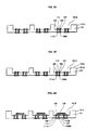
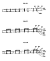
- Fig. 1 is a sectional view typically showing a semiconductor device 100 according to a first embodiment of the invention.
- the semiconductor device 100 is obtained by mounting a light emitting device 102 formed by an LED, for example, as an optical functional device, on a substrate 101 formed of Si, for example.
- the light emitting device 102 has a P layer, an N layer and an electrode formed thereon by using sapphire (Al 2 O 3 ) as a base material, and an upper surface thereof is provided with a light reflection preventing film 130 for preventing a reflection of a light.
- sapphire Al 2 O 3
- the light reflection preventing film 130 is a transparent film obtained by coating a dielectric film having a high light transmittance, in a single-layer or a multiplayer, through a vacuum evaporation method, spin coating process, or etc.
- a light irradiated from an inner part of the light emitting device 102 to an outside passes through the upper surface (a boundary surface for a refractive index) of the light emitting device 102 and proceeds in the air, therefore, a total reflection of the light can be prevented from being caused by a difference in the refractive index.
- the invention can also be applied to a semiconductor device having a structure in which a light receiving device is mounted, for example, instead of the light emitting device.
- the light reflection preventing film 130 can increase an intensity of a light which is incident from an outside and is received with a prevention of a reflection thereof.
- the total reflection is generated so that the emitted light cannot proceed to the outside of the light emitting device 102 depending on the angle of incidence.
- the light reflection preventing film 130 is formed on an upper surface to be a light emitting surface (a boundary surface for a refractive index) of the light emitting device 102.
- a light emitting surface a boundary surface for a refractive index
- the angle of incidence is equal to or greater than the critical angle, therefore, a light proceeding from the inner part of the light emitting device 102 to the outside is prevented from being reflected by the light reflection preventing film 130. Consequently, the light can be transmitted upward.
- an amount of the light emission of the light emitting device 102 itself is increased so that an intensity of a light transmitted from a light emitting surface is enhanced.
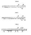
- the light reflection preventing film 140 is constituted by a single-layer or multilayer reflection preventing film in the same manner as the light reflection preventing film 130, and the reflection of the light can be prevented to relatively increase the amount of the light transmitted through the cover 103.
- the invention it is also possible to employ a structure in which both of the light reflection preventing films 130 and 140 are formed or either of the light reflection preventing films 130 and 140 is formed.
- the light reflection preventing film is formed on a lower surface of the cover 103 as well as the upper surface thereof, moreover, it is possible to increase a light transmittance, thereby enhancing an intensity of the light in the case in which a phosphor film 104 to be described below is formed by a substance having a higher refractive index than that of the glass, for example.
- the invention can also be applied to a semiconductor device having a structure in which a light receiving device is mounted instead of the light emitting device, for example.
- the light reflection preventing films 130 and 140 prevent a reflection of a light incident from an outside, thereby increasing an intensity of a light to be received.
- the phosphor film 104 is formed on the lower surface of the cover 103.
- the light emitting device LED
- the light emitting device is not directly coated with a phosphor film or a resin containing a phosphor in the semiconductor device 100 according to the first embodiment. Consequently, the radiation of the light emitting device 102 can be enhanced, resulting in suppression in the influence of deterioration in quality due to the heat generation of the light emitting device.
- the influence of deterioration due to the radiation from the light emitting device 102 and the irradiation of ultraviolet rays can be suppressed so that the quality of the semiconductor device can be improved and a lifetime can be prolonged.
- a concave portion 101B for mounting the light emitting device 102 is formed on the substrate 101 and the periphery of the concave portion 101B is bonded to the cover 103 so that the light emitting device 102 is sealed over the substrate 101. More specifically, in the structure, a space for sealing the light emitting device 102 is formed by the substrate 101 and the cover 103. Therefore, the space for sealing the light emitting device 102 can be brought into a pressure reducing state, for example, or can be filled with an inactive gas. Thus, the quality of the light emitting device 102 can be maintained and a lifetime can be prolonged.
- the substrate 101 When the substrate 101 is connected to the cover 103 through anode bonding, moreover, a space for sealing the light emitting device 102 is held more cleanly than that in the case in which they are bonded through an organic material such as a resin. Therefore, the quality of the light emitting device 102 can be enhanced, which is preferable.
- a reflector 105 for reflecting a light emitted from the light emitting device 102 is disposed together with the light emitting device 102 in the space (the concave portion 101B) in which the light emitting device 102 is sealed.
- the light emitting device 102 is disposed on a bump (Au bump) 106 formed of Au, for example, and is electrically connected to a via plug (through wiring) 107 formed to penetrate through a bottom face of the substrate 101 via the bump 106.
- a connecting layer 108A formed by an Ni/Au plated layer is provided on an opposite side to a side of the via plug 107 on which the light emitting device 102 is connected, and furthermore, a solder bump 108 is formed on the connecting layer 108A. More specifically, the via plug 107 is formed so that the light emitting device 102 and a connecting target on an outside of the space for sealing the light emitting device 102 can easily be connected to each other.
- a connecting layer formed by the Ni/Au plated layer for example, may be provided between the bump 106 and the via plug 107, moreover, it is not shown in the drawing.
- the reflector 105 is connected to a via plug (radiation wiring) 110 penetrating through the substrate 101. Therefore, the radiating property of the reflector 105 can be enhanced.
- the via plug 110 has the same structure as the via plug 107.
- the reflector 105 is connected to the via plug 110 formed to penetrate through the bottom face of the substrate 101 through a bump (Au bump) 109.
- the reflector 105 is cooled (radiated) through the via plug 110.
- the via plug 110 the solder bump 111 should be constituted to be connected to a mother board, resulting in an excellent radiating property, for example.
- the substrate 101 is formed of Si, for example, it can easily be processed to have a fine shape, which is preferable.
- Si has such a feature that micromachining can be carried out more easily than a material such as ceramic.
- the substrate 101 is formed of Si, moreover, it is also possible to carry out anode bonding together with the cover 103 formed of a glass (a borosilicate glass).
- an oxide film (a silicon oxide film) 101A is formed on a surface of the substrate 101, and the substrate 101 is insulated from the via plugs 107 and 110 and the bumps 106 and 109, for example.
- a sapphire wafer having a predetermined thickness is created in a step 1.
- Sapphire is excellent in a light transparency and a heat resistance, and particularly, also has such a durability that it is deteriorated with difficulty even if a light is converted into a heat to carry out heating to a high temperature with respect to a blue light emitting member. Therefore, the sapphire is suitable for an LED substrate.
- a thin film constituted by a compound such as gallium nitride (NGa) is epitaxially grown on the sapphire substrate by using a film forming method such as a vapor phase growth, thereby forming a P-type semiconductor and an N-type semiconductor.
- NGa gallium nitride
- a step 3 furthermore, an electrode is formed on each of the P-type semiconductor and the N-type semiconductor.
- a surface (a back surface) on an opposite side to a surface of the sapphire substrate on which the electrode is formed is coated with a light reflection preventing film.
- the light reflection preventing film is obtained by coating a dielectric films having a high light transmittance, in a single-layer or a multiplayer, through a vacuum evaporation method, spin coating process, or etc.
- each light emitting device formed on the sapphire substrate is cut into individual pieces by dicing. Consequently, there is obtained the light emitting device 102 on which the light reflection preventing film 130 is formed.
- the light emitting device 102 is mounted by setting, as an upper surface, a surface on which the light reflection preventing film 130 is formed.
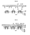
- the substrate 101 formed of Si is etched and patterned to form the concave portion 101B for disposing a light emitting device and via holes 107A and 110A penetrating through the substrate 101 which serve to form the via plugs 107 and 110.
- the oxide film (which is also referred to as a silicon oxide film or a thermal oxide film) 101A is formed by a thermal CVD method, for example, on a surface of the substrate 101 including an internal wall surface of the concave portion 101B and internal wall surfaces of the via holes 107A and 110A.
- the via plugs 107 and 110 are formed on the via holes 107A and 110A by a Cu plating method (such as a semiadditive method), for example, respectively.
- connecting layers 106A, 109A, 108A and 111A formed of Ni/Au, for example, are provided by a plating method, for example.
- the connecting layers 106A and 109A are formed on a side of the concave portion 101B of the via plugs 107 and 110 respectively, and the connecting layers 108A and 111A are formed on an opposite side of the via plugs 107 and 110 to the concave portion 101B respectively.
- the bumps (Au bumps) 106 and 109 are formed on the connecting layers 106A and 109A.
- the connecting layers 106A and 109A are omitted.
- the oxide film 101A provided on a surface of a convex portion 101C around the concave portion 101B is removed by mask etching, for example.
- a cover formed of a glass is bonded, at a subsequent step, to a portion from which the oxide film is removed at the step.
- the light emitting device 102 having the light reflection preventing film 130 formed thereon by the steps 1 to 5 is disposed in the concave portion 101B by setting, as an upper surface, a surface on which the light reflection preventing film 130 is formed.
- thermal compression bonding or ultrasonic bonding is used to electrically bond the light emitting device 102 to the bump 106 and to electrically connect the light emitting device 102 to the via plug 107 through the bump 106.
- the reflector 105 obtained by forming a reflecting film of Ag or Al on a surface of an alloy of Fe, Ni or Co, for example, is disposed in the concave portion 101B.
- thermal compression bonding or ultrasonic bonding is used to bond the reflector 105 to the bump 109 and to connect the reflector 105 to the via plug 110 through the bump 109.
- an upper surface of the plate-shaped cover 103 which is formed by a borosilicate glass, for example, and has a transparency is coated, in a multilayer, with a dielectric film having a high light transmittance by a vacuum evaporation method, thereby forming the light reflection preventing film 140.
- the phosphor film 104 is formed on a lower surface of the cover 103 by patterning. In the method of manufacturing a semiconductor device according to the first embodiment, the light reflection preventing film 140 and the phosphor film 104 are formed on the upper and lower surfaces of the plate-shaped cover 103 as described above.
- a uniformity of a thickness of each of the light reflection preventing film 140 and the phosphor film 104 can be maintained to be high. Therefore, it is possible to enhance an intensity of a light emission and a uniformity of a luminescent color in the semiconductor device.
- the phosphor film 104 should not be formed in a portion in which the cover 103 is bonded to the substrate 101 but the phosphor film 104 should be patterned in such a manner that the cover 103 directly comes in contact with the substrate 101.
- the cover 103 and the substrate 101 are bonded to each other through anode bonding, for example, and a structure for sealing the light emitting device 102 over the substrate 101 is formed.
- the anode bonding is carried out by applying a high voltage between the cover 103 and the substrate 101 and raising the temperatures of the cover 103 and the substrate 101.
- Si constituting the substrate is coupled to oxygen in the glass constituting the cover so that stable bonding with a great bonding force is performed.
- a gas and an impurity which contaminate a space for sealing the light emitting device 102 are rarely generated.
- solder bumps 108 and 111 are formed on the connecting layers 108A and 111A, respectively.
- the substrate 101 and the cover 103 are cut into individual pieces by dicing. Consequently, the semiconductor device 100 (see Fig. 2) described above is finished.
- the light reflection preventing film may be formed on a side wall of the cover 103 in addition to the upper surface thereof. In that case, only the cover 103 may be subjected to half dicing when cutting the cover 103 and the side surface of the cover 103 may be then coated with a dielectric film in a multilayer to form the light reflection preventing film.
- the semiconductor device according to the invention is not restricted to the structure described in the first embodiment but various structures can be employed as will be described below, for example.
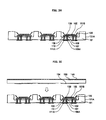
- Fig. 4 is a sectional view typically showing a semiconductor device 200 according to a second embodiment of the invention.
- the semiconductor device 200 is obtained by mounting a light emitting device 202 formed by an LED, for example, on a substrate 201 formed of Si, for example.
- the light emitting device 202 has a P layer, an N layer and an electrode formed thereon by using sapphire (Al 2 O 3 ) as a base material, and an upper surface thereof is provided with a light reflection preventing film 230 for preventing a reflection of a light.
- the light reflection preventing film 230 is a transparent film obtained by coating a dielectric film having a high light transmittance, in a single-layer or a multiplayer, through a vacuum evaporation method, spin coating process, or etc.
- the light reflection preventing film 240 is constituted by a single-layer or multilayer reflection preventing film in the same manner as the light reflection preventing film 230, and the reflection of the light can be prevented to relatively increase the amount of the light transmitted through the cover 203.
- the invention it is also possible to employ a structure in which both of the light reflection preventing films 230 and 240 are formed or either of the light reflection preventing films 230 and 240 is formed.
- the light reflection preventing film is formed on a lower surface of the cover 203 as well as the upper surface thereof, moreover, it is possible to increase a light transmittance, thereby enhancing an intensity of the light in the case in which a phosphor film 204 to be described below is formed by a substance having a higher refractive index than that of the glass, for example.
- the invention can also be applied to a semiconductor device having a structure in which a light receiving device is mounted instead of the light emitting device, for example.
- the light reflection preventing films 230 and 240 prevent a reflection of a light incident from an outside, thereby increasing an intensity of a light to be received.
- the phosphor film 204 is formed on a lower surface of the cover 203.
- the substrate 201, the light emitting device 202, the cover 203 and the phosphor film 204 according to the second embodiment correspond to the substrate 101, the light emitting device 102, the cover 103 and the phosphor film 104 according to the first embodiment, and the semiconductor device 200 according to the second embodiment has the same advantages as those of the semiconductor device 100 according to the first embodiment.
- the light emitting device is not directly coated with a phosphor film or a resin containing a phosphor in the semiconductor device 200. Consequently, the radiation of the light emitting device 202 can be enhanced, resulting in a suppression in the influence of a deterioration in quality due to the heat generation of the light emitting device.
- the influence of a deterioration due to the radiation from the light emitting device 202 and the irradiation of ultraviolet rays can be suppressed so that the quality of the semiconductor device can be improved and a lifetime can be prolonged.
- the phosphor film is formed on the almost plate-shaped cover 203 by a printing method, for example. Therefore, the semiconductor device 200 has a feature that a thickness of the phosphor film has a high uniformity. More specifically, in the semiconductor device 200 according to the second embodiment, the phosphor film 204 is formed on the plate-shaped cover 203. Therefore, it is possible to form the phosphor film 204 with a high uniformity of the thickness by using the printing method, for example. In the semiconductor device 200 according to the second embodiment, furthermore, it is not necessary to form a phosphor film on a side surface of the light emitting device 202. Therefore, the semiconductor device 200 has a feature that an intensity of a light emission and a uniformity of a luminescent color are enhanced.
- the light emitting device 202 is disposed on a bump (Au bump) 206 formed of Au, for example, and is electrically connected to a via plug (through wiring) 207 formed to penetrate through a bottom face of the substrate 201 via the bump 206.
- a connecting layer 208A formed by an Ni/Au plated layer is provided on an opposite side to a side of the via plug 207 on which the light emitting device 202 is connected, and furthermore, a solder bump 208 is formed on the connecting layer 208A. More specifically, the via plug 207 is formed so that the light emitting device 202 and a connecting target on an outside of the space for sealing the light emitting device 202 can easily be connected to each other. Although a connecting layer formed by the Ni/Au plated layer, for example, may be formed between the bump 206 and the via plug 207, moreover, it is not shown in the drawing.
- an oxide film (a silicon oxide film) 201A is formed on a surface of the substrate 201 and the substrate 201 is insulated from the via plug 207 and the bump 206, for example.
- the semiconductor device 200 according to the second embodiment is different from the semiconductor device 100 according to the first embodiment in the following respects and has advantages which are peculiar to the second embodiment.
- the semiconductor device 200 has a reflector 205 (corresponding to the reflector 105) for reflecting a light emitted from the light emitting device 202, and furthermore, the reflector 205 forms a sealing space 201B for sealing the light emitting device 202 together with the substrate 201 and the cover 203.
- one of ends of the reflector 205 is bonded to the substrate 201 through a bonding layer 210 such as Au which is formed on the substrate 201.
- the other end of the reflector 205 is bonded to the cover 203 through a bonding layer 209 formed of Au, for example. More specifically, the reflector 205 is bonded to both the substrate 201 and the cover 203 so that the sealing space 201B for sealing the light emitting device 202 is formed.
- the sealing space 201B can be brought into a pressure reducing state or can be filled with an inactive gas, for example.
- the quality of the light emitting device 202 can be maintained and a lifetime can be prolonged.
- a radiation wiring corresponding to the via plug 110 described in the first embodiment is formed on the substrate 201 and is connected to the reflector 205 so that a radiating property of the reflector 205 can be enhanced (the same structure as that in the first embodiment).
- the structure (shape) of the substrate 201 is simpler than the substrate 101 and has a feature that the substrate 201 can easily be processed. With the structure, moreover, the reflector is exposed to the outside air. Therefore, there is an advantage that the radiating property is more excellent than that of the semiconductor device 100.
- the substrate 201 formed of Si is etched and patterned to form a via hole 207A penetrating through the substrate 201 which serves to form the via plug 207.
- an oxide film (which is also referred to as a silicon oxide film or the thermal oxide film) 201A is formed by a thermal CVD method, for example, on a surface of the substrate 201 including an internal wall surface of the via hole 207A.
- the via plug 207 is formed in the via hole 207A by a Cu plating method (such as a semiadditive method), for example.
- connecting layers 206A and 208A formed of Ni/Au are provided for the via plug 207 by a plating method, for example.
- the connecting layer 206A is formed on a first side on which a light emitting device is to be mounted at a subsequent step and the connecting layer 208A is formed on a second side which is opposite to the first side.
- the bonding layer 210 formed of Au for example, which serves to bond the reflector at a subsequent step is provided on the first side of the substrate 201 by a sputtering method or a plating method.
- the connecting layers 206A and 209A are omitted.
- the bump (Au bump) 206 is formed on the connecting layer 206A.
- the light emitting device 202 formed by an LED is disposed on the substrate 201, for example.
- thermal compression bonding or ultrasonic bonding is used to electrically bond the light emitting device 202 having the light reflection preventing film 230 formed thereon by the steps 1 to 5 to the bump 206 and to electrically connect the light emitting device 202 and the via plug 207 to each other through the bump 206.
- the substrate 201 is cut by dicing.
- the substrate 201 having the light emitting device 202 mounted thereon is cut into individual pieces.
- the phosphor film 204 is formed on a lower surface of the cover 203 by patterning. In the method of manufacturing a semiconductor device according to the second embodiment, the light reflection preventing film 240 and the phosphor film 204 are formed on the upper and lower surfaces of the plate-shaped cover 203 as described above.
- a uniformity of a thickness of each of the light reflection preventing film 240 and the phosphor film 204 can be maintained to be high. Therefore, it is possible to enhance an intensity of a light emission and a uniformity of a luminescent color in the semiconductor device 200.
- the bonding layer 209 formed of Au, for example, through which the reflector 205 is to be bonded to the cover 203 at a subsequent step is provided by the sputtering method, for example.
- an upper end of the reflector 205 obtained by forming a reflecting film of Ag or A1 on a surface of an alloy of Fe, Ni or Co, for example, is bonded to the bonding layer 209.
- the reflector 205 is bonded to the bonding layer 209 by using thermal compression bonding or ultrasonic bonding, for example.
- a lower end of the reflector 205 bonded to the cover 203 is bonded to the substrate 201 having the light emitting device 202 mounted thereon.
- the reflector 205 is bonded to the bonding layer 210 by using the thermal compression bonding or the ultrasonic bonding, for example.
- the sealing space 201B in which the light emitting device 202 is sealed is formed so that the light emitting device 202 is sealed over the substrate 201.
- solder bump 208 is formed on the connecting layer 208A.
- the cover 203 is cut into individual pieces by dicing. Consequently, the semiconductor device 200 (see Fig. 4) described above can be formed.
- the structure (shape) of the substrate 201 is simpler than that of the substrate 101 according to the first embodiment, and furthermore, the reflector is exposed to the outside air. Therefore, the semiconductor device 200 has a feature that a radiating property is more excellent than that of the semiconductor device 100 according to the first embodiment.
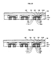
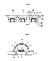
- Fig. 6 is a view showing a semiconductor device according to a third embodiment. As shown in Fig. 6, in a semiconductor device 300, a light emitting device 302 is fixed onto a substrate 301 through a bonding layer 320. A light reflection preventing film 330 is formed on an upper surface of the light emitting device 302.
- the substrate 301 is provided with a via plug 307 penetrating from an upper surface to a lower surface, and a lower end of the via plug 307 is electrically connected to a wiring pattern 308 formed on a lower surface of the substrate 301. Furthermore, an upper end of the via plug 307 is connected to an electrode (not shown) of the light emitting device 302 through a bonding wire 322.
- the cover 303 is formed to have an inner part taking a hemispherical shape, and has a light reflection preventing film 340 formed on an outer peripheral surface and a phosphor film 304 formed on an inner peripheral surface.
- the light reflection preventing films 330 and 340 are transparent films formed by coating a dielectric film having a high light transmittance in a multilayer through a vacuum evaporation method, for example, in the same manner as in the first and second embodiments. Accordingly, the light reflection preventing films 330 and 340 are formed by a single-layer or multilayer reflection preventing film in the same manner as in the first and second embodiments, and it is possible to relatively increase the amount of a light transmitted through the light emitting device 302 and the cover 303 by preventing a reflection of the light.
- the structure in which the light reflection preventing film is formed on the inner peripheral surface of the cover 303 taking the hemispherical shape as well as the outer peripheral surface thereof moreover, it is possible to increase a light transmittance, thereby enhancing a light intensity in the case in which the phosphor film 304 is constituted by a substance having a higher refractive index than that of a glass, for example.
- the invention can also be applied to a semiconductor device having a structure in which a light receiving device is mounted instead of the light emitting device, for example.
- the light reflection preventing films 330 and 340 can prevent a reflection of a light which is incident from an outside, thereby increasing an intensity of the light to be received.
- a light reflection preventing film is formed by a single-layer or multilayer reflection preventing film using a vacuum evaporation method or spin coating process.
- a vacuum evaporation method or spin coating process it is a matter of course that other thin film forming methods may be used to form the light reflection preventing film.
- the cover for sealing the light emitting device which takes the shapes of the plate and the hemisphere has been taken as an example in the first to third embodiments.
- the shape of the cover is not restricted thereto. It is a matter of course that the cover may take a shape of a convex lens or a bottomed cylinder, for example.
Applications Claiming Priority (1)
| Application Number | Priority Date | Filing Date | Title |
|---|---|---|---|
| JP2006025649A JP4996101B2 (ja) | 2006-02-02 | 2006-02-02 | 半導体装置及び半導体装置の製造方法 |
Publications (1)
| Publication Number | Publication Date |
|---|---|
| EP1816687A2 true EP1816687A2 (de) | 2007-08-08 |
Family
ID=38038555
Family Applications (1)
| Application Number | Title | Priority Date | Filing Date |
|---|---|---|---|
| EP07002224A Withdrawn EP1816687A2 (de) | 2006-02-02 | 2007-02-01 | Halbleiterbauelement und Verfahren zur Herstellung eines Halbleiterbauelements |
Country Status (4)
| Country | Link |
|---|---|
| US (1) | US7825423B2 (de) |
| EP (1) | EP1816687A2 (de) |
| JP (1) | JP4996101B2 (de) |
| TW (1) | TW200805707A (de) |
Cited By (3)
| Publication number | Priority date | Publication date | Assignee | Title |
|---|---|---|---|---|
| WO2009036731A2 (de) | 2007-09-21 | 2009-03-26 | Osram Opto Semiconductors Gmbh | Strahlungsemittierendes bauelement |
| EP2048717A1 (de) * | 2007-10-10 | 2009-04-15 | Unity Opto Technology Co., Ltd. | Leuchtdiodenstruktur |
| EP2597689A4 (de) * | 2010-07-22 | 2016-05-11 | Kyocera Corp | Lichtemittierende vorrichtung |
Families Citing this family (35)
| Publication number | Priority date | Publication date | Assignee | Title |
|---|---|---|---|---|
| KR100883075B1 (ko) * | 2007-03-02 | 2009-02-10 | 엘지전자 주식회사 | 전계발광소자 |
| JP5089336B2 (ja) | 2007-10-29 | 2012-12-05 | 新光電気工業株式会社 | パッケージ用シリコン基板 |
| JP4912275B2 (ja) | 2007-11-06 | 2012-04-11 | 新光電気工業株式会社 | 半導体パッケージ |
| JP2010074117A (ja) * | 2007-12-07 | 2010-04-02 | Panasonic Electric Works Co Ltd | 発光装置 |
| KR100998009B1 (ko) * | 2008-03-12 | 2010-12-03 | 삼성엘이디 주식회사 | 발광 다이오드 패키지 및 그 제조 방법 |
| WO2009119038A2 (en) * | 2008-03-28 | 2009-10-01 | Panasonic Corporation | Molded resin product, semiconductor light-emitting source, lighting device, and method for manufacturing molded resin product |
| DE102008025491A1 (de) * | 2008-05-28 | 2009-12-03 | Osram Opto Semiconductors Gmbh | Optoelektronisches Halbleiterbauteil und Leiterplatte |
| US8058669B2 (en) * | 2008-08-28 | 2011-11-15 | Taiwan Semiconductor Manufacturing Company, Ltd. | Light-emitting diode integration scheme |
| JP2010135488A (ja) * | 2008-12-03 | 2010-06-17 | Toshiba Corp | 発光装置及びその製造方法 |
| DE102009005547A1 (de) * | 2009-01-20 | 2010-07-29 | R. Stahl Schaltgeräte GmbH | Gekapselte Leuchtdiodenanordnung |
| KR101064026B1 (ko) * | 2009-02-17 | 2011-09-08 | 엘지이노텍 주식회사 | 발광 디바이스 패키지 및 그 제조방법 |
| JP5327042B2 (ja) * | 2009-03-26 | 2013-10-30 | 豊田合成株式会社 | Ledランプの製造方法 |
| US20100301728A1 (en) * | 2009-06-02 | 2010-12-02 | Bridgelux, Inc. | Light source having a refractive element |
| KR101714042B1 (ko) * | 2010-08-05 | 2017-03-08 | 엘지이노텍 주식회사 | 발광 소자 패키지 |
| WO2012124473A1 (ja) * | 2011-03-15 | 2012-09-20 | 京セラ株式会社 | 発光装置 |
| JP5769482B2 (ja) * | 2011-04-18 | 2015-08-26 | セイコーインスツル株式会社 | ガラス封止型パッケージの製造方法、及び光学デバイス |
| JP2013004901A (ja) * | 2011-06-21 | 2013-01-07 | Nippon Kasei Chem Co Ltd | Ledデバイス |
| TW201310126A (zh) * | 2011-08-18 | 2013-03-01 | Hon Hai Prec Ind Co Ltd | 發光裝置 |
| CN103050583A (zh) * | 2011-10-14 | 2013-04-17 | 展晶科技(深圳)有限公司 | 发光二极管的封装方法 |
| KR101887942B1 (ko) * | 2012-05-07 | 2018-08-14 | 삼성전자주식회사 | 발광소자 |
| JP6139071B2 (ja) * | 2012-07-30 | 2017-05-31 | 日亜化学工業株式会社 | 発光装置とその製造方法 |
| DE102013104240B4 (de) | 2013-04-26 | 2015-10-22 | R. Stahl Schaltgeräte GmbH | Explosionsgeschützte Anordnung elektrischer und/oder elektronischer Bauelemente |
| JP6490932B2 (ja) * | 2013-09-16 | 2019-03-27 | エルジー イノテック カンパニー リミテッド | 発光素子パッケージ |
| DE102013111374A1 (de) * | 2013-10-15 | 2015-04-16 | R. Stahl Schaltgeräte GmbH | Explosionsgeschützte Anordnung für elektrische und/oder elektronische Bauelemente |
| CN104124324B (zh) * | 2014-08-06 | 2017-03-01 | 华中科技大学 | 一种led封装玻璃及其制备方法和应用 |
| US10681777B2 (en) * | 2016-04-01 | 2020-06-09 | Infineon Technologies Ag | Light emitter devices, optical filter structures and methods for forming light emitter devices and optical filter structures |
| US10347814B2 (en) | 2016-04-01 | 2019-07-09 | Infineon Technologies Ag | MEMS heater or emitter structure for fast heating and cooling cycles |
| US10559723B2 (en) | 2017-08-25 | 2020-02-11 | Rohm Co., Ltd. | Optical device |
| BR112020012418A2 (pt) * | 2018-01-29 | 2020-11-24 | Philip Morris Products S.A. | unidade de iluminação para sistemas geradores de aerossol |
| US11758948B2 (en) | 2018-01-29 | 2023-09-19 | Altria Client Services Llc | Lighting unit for aerosol-generating systems |
| US11178392B2 (en) * | 2018-09-12 | 2021-11-16 | Apple Inc. | Integrated optical emitters and applications thereof |
| EP3888204B1 (de) | 2019-02-04 | 2022-12-14 | Apple Inc. | Vertikale emitter mit integrierten mikrolinsen |
| JP7239840B2 (ja) * | 2020-08-31 | 2023-03-15 | 日亜化学工業株式会社 | 発光装置の製造方法 |
| WO2023042461A1 (ja) * | 2021-09-14 | 2023-03-23 | ソニーグループ株式会社 | 半導体発光デバイス |
| CN114864796A (zh) * | 2022-07-05 | 2022-08-05 | 至芯半导体(杭州)有限公司 | 一种紫外器件封装结构及制作方法 |
Family Cites Families (18)
| Publication number | Priority date | Publication date | Assignee | Title |
|---|---|---|---|---|
| JPS4846288A (de) * | 1971-10-13 | 1973-07-02 | ||
| JPH0328467Y2 (de) * | 1985-12-28 | 1991-06-19 | ||
| JPH06350132A (ja) * | 1993-06-08 | 1994-12-22 | Victor Co Of Japan Ltd | 半導体発光素子アレイ |
| US6784463B2 (en) * | 1997-06-03 | 2004-08-31 | Lumileds Lighting U.S., Llc | III-Phospide and III-Arsenide flip chip light-emitting devices |
| JP2003110146A (ja) * | 2001-07-26 | 2003-04-11 | Matsushita Electric Works Ltd | 発光装置 |
| WO2004001862A1 (ja) * | 2002-06-19 | 2003-12-31 | Sanken Electric Co., Ltd. | 半導体発光装置及びその製法並びに半導体発光装置用リフレクタ |
| US7224000B2 (en) * | 2002-08-30 | 2007-05-29 | Lumination, Llc | Light emitting diode component |
| JP4280050B2 (ja) * | 2002-10-07 | 2009-06-17 | シチズン電子株式会社 | 白色発光装置 |
| KR101173198B1 (ko) * | 2002-12-25 | 2012-08-10 | 도꾸리쯔교세이호징 가가꾸 기쥬쯔 신꼬 기꼬 | 발광소자장치, 수광소자장치, 광학장치, 플루오르화물결정, 플루오르화물 결정의 제조방법 및 도가니 |
| KR20040092512A (ko) * | 2003-04-24 | 2004-11-04 | (주)그래픽테크노재팬 | 방열 기능을 갖는 반사판이 구비된 반도체 발광장치 |
| EP1484802B1 (de) * | 2003-06-06 | 2018-06-13 | Stanley Electric Co., Ltd. | Optische Halbleitervorrichtung |
| JP4138586B2 (ja) * | 2003-06-13 | 2008-08-27 | スタンレー電気株式会社 | 光源用ledランプおよびこれを用いた車両用前照灯 |
| US7560820B2 (en) * | 2004-04-15 | 2009-07-14 | Saes Getters S.P.A. | Integrated getter for vacuum or inert gas packaged LEDs |
| JP4996463B2 (ja) * | 2004-06-30 | 2012-08-08 | クリー インコーポレイテッド | 発光デバイスをパッケージするためのチップスケール方法およびチップスケールにパッケージされた発光デバイス |
| US7470926B2 (en) * | 2004-09-09 | 2008-12-30 | Toyoda Gosei Co., Ltd | Solid-state optical device |
| US7365371B2 (en) * | 2005-08-04 | 2008-04-29 | Cree, Inc. | Packages for semiconductor light emitting devices utilizing dispensed encapsulants |
| US7798678B2 (en) * | 2005-12-30 | 2010-09-21 | 3M Innovative Properties Company | LED with compound encapsulant lens |
| US7521728B2 (en) * | 2006-01-20 | 2009-04-21 | Cree, Inc. | Packages for semiconductor light emitting devices utilizing dispensed reflectors and methods of forming the same |
-
2006
- 2006-02-02 JP JP2006025649A patent/JP4996101B2/ja not_active Expired - Fee Related
-
2007
- 2007-02-01 EP EP07002224A patent/EP1816687A2/de not_active Withdrawn
- 2007-02-01 US US11/700,761 patent/US7825423B2/en not_active Expired - Fee Related
- 2007-02-02 TW TW096103824A patent/TW200805707A/zh unknown
Cited By (6)
| Publication number | Priority date | Publication date | Assignee | Title |
|---|---|---|---|---|
| WO2009036731A2 (de) | 2007-09-21 | 2009-03-26 | Osram Opto Semiconductors Gmbh | Strahlungsemittierendes bauelement |
| WO2009036731A3 (de) * | 2007-09-21 | 2009-05-28 | Osram Opto Semiconductors Gmbh | Strahlungsemittierendes bauelement |
| US8373186B2 (en) | 2007-09-21 | 2013-02-12 | Osram Opto Semiconductors Gmbh | Radiation-emitting component |
| US8963181B2 (en) | 2007-09-21 | 2015-02-24 | Osram Opto Semiconductors Gmbh | Radiation-emitting component |
| EP2048717A1 (de) * | 2007-10-10 | 2009-04-15 | Unity Opto Technology Co., Ltd. | Leuchtdiodenstruktur |
| EP2597689A4 (de) * | 2010-07-22 | 2016-05-11 | Kyocera Corp | Lichtemittierende vorrichtung |
Also Published As
| Publication number | Publication date |
|---|---|
| US20070194712A1 (en) | 2007-08-23 |
| TW200805707A (en) | 2008-01-16 |
| JP2007208041A (ja) | 2007-08-16 |
| JP4996101B2 (ja) | 2012-08-08 |
| US7825423B2 (en) | 2010-11-02 |
Similar Documents
| Publication | Publication Date | Title |
|---|---|---|
| EP1816687A2 (de) | Halbleiterbauelement und Verfahren zur Herstellung eines Halbleiterbauelements | |
| JP5526232B2 (ja) | モールドされた反射側壁コーティングを備える発光ダイオード | |
| JP5209177B2 (ja) | 半導体装置および半導体装置の製造方法 | |
| TWI420688B (zh) | 用以移除一半導體發光裝置之成長基板的方法 | |
| EP2264797B1 (de) | Lichtemittierende Vorrichtung | |
| JP4589604B2 (ja) | 発光素子に自己整合及び自己露光フォトレジストパターンを作製する方法 | |
| US20110049545A1 (en) | Led package with phosphor plate and reflective substrate | |
| CN104953016A (zh) | 半导体发光装置 | |
| US20090236619A1 (en) | Light Emitting Diodes with Light Filters | |
| EP2943986B1 (de) | Leuchtdiode mit ausgeformtem aufwachssubstrat zur horizontalemission und verfahren zu seiner herstellung | |
| US20150280078A1 (en) | White flip chip light emitting diode (fc led) and fabrication method | |
| CN102324452A (zh) | 用于p型氮化物发光装置的超薄欧姆接触及其形成方法 | |
| US11081626B2 (en) | Light emitting diode packages | |
| JP2004111882A (ja) | 発光装置 | |
| US7884380B2 (en) | Semiconductor light emitting device | |
| JP5451534B2 (ja) | 半導体発光装置および半導体発光装置の製造方法 | |
| JP4846505B2 (ja) | 発光装置およびその製造方法 | |
| JP2007208301A (ja) | Led照明装置 | |
| KR101960432B1 (ko) | 반도체 발광소자 | |
| JP2013197310A (ja) | 発光装置 | |
| JP4820133B2 (ja) | 発光装置 | |
| JP2008166661A (ja) | 半導体発光装置 | |
| CN104966777A (zh) | 半导体发光装置及其制造方法 | |
| JP4925346B2 (ja) | 発光装置 | |
| JP2021507527A (ja) | 変換素子を製造する方法および変換素子 |
Legal Events
| Date | Code | Title | Description |
|---|---|---|---|
| PUAI | Public reference made under article 153(3) epc to a published international application that has entered the european phase |
Free format text: ORIGINAL CODE: 0009012 |
|
| AK | Designated contracting states |
Kind code of ref document: A2 Designated state(s): AT BE BG CH CY CZ DE DK EE ES FI FR GB GR HU IE IS IT LI LT LU LV MC NL PL PT RO SE SI SK TR |
|
| AX | Request for extension of the european patent |
Extension state: AL BA HR MK YU |
|
| STAA | Information on the status of an ep patent application or granted ep patent |
Free format text: STATUS: THE APPLICATION IS DEEMED TO BE WITHDRAWN |
|
| 18D | Application deemed to be withdrawn |
Effective date: 20120901 |