EP1816233B1 - Verfahren zur Herstellung einer Schicht mit einem vorgegebenen Schichtdickenprofil - Google Patents
Verfahren zur Herstellung einer Schicht mit einem vorgegebenen Schichtdickenprofil Download PDFInfo
- Publication number
- EP1816233B1 EP1816233B1 EP07008531A EP07008531A EP1816233B1 EP 1816233 B1 EP1816233 B1 EP 1816233B1 EP 07008531 A EP07008531 A EP 07008531A EP 07008531 A EP07008531 A EP 07008531A EP 1816233 B1 EP1816233 B1 EP 1816233B1
- Authority
- EP
- European Patent Office
- Prior art keywords
- layer
- ion beam
- profile
- thickness profile
- current density
- Prior art date
- Legal status (The legal status is an assumption and is not a legal conclusion. Google has not performed a legal analysis and makes no representation as to the accuracy of the status listed.)
- Expired - Lifetime
Links
- 238000000034 method Methods 0.000 title claims description 50
- 238000004519 manufacturing process Methods 0.000 title claims description 9
- 238000010884 ion-beam technique Methods 0.000 claims description 46
- 238000005530 etching Methods 0.000 claims description 15
- 238000009826 distribution Methods 0.000 claims description 6
- 239000000758 substrate Substances 0.000 claims description 6
- 238000005259 measurement Methods 0.000 claims description 5
- XKRFYHLGVUSROY-UHFFFAOYSA-N Argon Chemical compound [Ar] XKRFYHLGVUSROY-UHFFFAOYSA-N 0.000 claims description 4
- 239000003990 capacitor Substances 0.000 claims description 4
- 229910052786 argon Inorganic materials 0.000 claims description 2
- 229910052751 metal Inorganic materials 0.000 description 11
- 239000002184 metal Substances 0.000 description 11
- 230000008901 benefit Effects 0.000 description 5
- 238000000151 deposition Methods 0.000 description 4
- 230000008021 deposition Effects 0.000 description 4
- 238000004544 sputter deposition Methods 0.000 description 4
- 239000000463 material Substances 0.000 description 3
- 239000012528 membrane Substances 0.000 description 3
- 239000010409 thin film Substances 0.000 description 3
- 238000005229 chemical vapour deposition Methods 0.000 description 2
- 238000002848 electrochemical method Methods 0.000 description 2
- 238000012545 processing Methods 0.000 description 2
- 230000006978 adaptation Effects 0.000 description 1
- 239000000654 additive Substances 0.000 description 1
- 230000000996 additive effect Effects 0.000 description 1
- 239000000919 ceramic Substances 0.000 description 1
- 239000004020 conductor Substances 0.000 description 1
- 238000012937 correction Methods 0.000 description 1
- 230000007547 defect Effects 0.000 description 1
- 230000001419 dependent effect Effects 0.000 description 1
- 239000006185 dispersion Substances 0.000 description 1
- 238000006073 displacement reaction Methods 0.000 description 1
- 230000000694 effects Effects 0.000 description 1
- 230000005284 excitation Effects 0.000 description 1
- 239000004922 lacquer Substances 0.000 description 1
- 238000001459 lithography Methods 0.000 description 1
- 238000004377 microelectronic Methods 0.000 description 1
- 229910021420 polycrystalline silicon Inorganic materials 0.000 description 1
- 229920005591 polysilicon Polymers 0.000 description 1
- 230000009897 systematic effect Effects 0.000 description 1
- 238000013519 translation Methods 0.000 description 1
- WFKWXMTUELFFGS-UHFFFAOYSA-N tungsten Chemical compound [W] WFKWXMTUELFFGS-UHFFFAOYSA-N 0.000 description 1
- 229910052721 tungsten Inorganic materials 0.000 description 1
- 239000010937 tungsten Substances 0.000 description 1
Images


Classifications
-
- H—ELECTRICITY
- H01—ELECTRIC ELEMENTS
- H01J—ELECTRIC DISCHARGE TUBES OR DISCHARGE LAMPS
- H01J37/00—Discharge tubes with provision for introducing objects or material to be exposed to the discharge, e.g. for the purpose of examination or processing thereof
- H01J37/30—Electron-beam or ion-beam tubes for localised treatment of objects
- H01J37/305—Electron-beam or ion-beam tubes for localised treatment of objects for casting, melting, evaporating, or etching
-
- C—CHEMISTRY; METALLURGY
- C23—COATING METALLIC MATERIAL; COATING MATERIAL WITH METALLIC MATERIAL; CHEMICAL SURFACE TREATMENT; DIFFUSION TREATMENT OF METALLIC MATERIAL; COATING BY VACUUM EVAPORATION, BY SPUTTERING, BY ION IMPLANTATION OR BY CHEMICAL VAPOUR DEPOSITION, IN GENERAL; INHIBITING CORROSION OF METALLIC MATERIAL OR INCRUSTATION IN GENERAL
- C23C—COATING METALLIC MATERIAL; COATING MATERIAL WITH METALLIC MATERIAL; SURFACE TREATMENT OF METALLIC MATERIAL BY DIFFUSION INTO THE SURFACE, BY CHEMICAL CONVERSION OR SUBSTITUTION; COATING BY VACUUM EVAPORATION, BY SPUTTERING, BY ION IMPLANTATION OR BY CHEMICAL VAPOUR DEPOSITION, IN GENERAL
- C23C14/00—Coating by vacuum evaporation, by sputtering or by ion implantation of the coating forming material
- C23C14/58—After-treatment
- C23C14/5826—Treatment with charged particles
- C23C14/5833—Ion beam bombardment
-
- C—CHEMISTRY; METALLURGY
- C23—COATING METALLIC MATERIAL; COATING MATERIAL WITH METALLIC MATERIAL; CHEMICAL SURFACE TREATMENT; DIFFUSION TREATMENT OF METALLIC MATERIAL; COATING BY VACUUM EVAPORATION, BY SPUTTERING, BY ION IMPLANTATION OR BY CHEMICAL VAPOUR DEPOSITION, IN GENERAL; INHIBITING CORROSION OF METALLIC MATERIAL OR INCRUSTATION IN GENERAL
- C23C—COATING METALLIC MATERIAL; COATING MATERIAL WITH METALLIC MATERIAL; SURFACE TREATMENT OF METALLIC MATERIAL BY DIFFUSION INTO THE SURFACE, BY CHEMICAL CONVERSION OR SUBSTITUTION; COATING BY VACUUM EVAPORATION, BY SPUTTERING, BY ION IMPLANTATION OR BY CHEMICAL VAPOUR DEPOSITION, IN GENERAL
- C23C14/00—Coating by vacuum evaporation, by sputtering or by ion implantation of the coating forming material
- C23C14/58—After-treatment
- C23C14/5873—Removal of material
-
- C—CHEMISTRY; METALLURGY
- C23—COATING METALLIC MATERIAL; COATING MATERIAL WITH METALLIC MATERIAL; CHEMICAL SURFACE TREATMENT; DIFFUSION TREATMENT OF METALLIC MATERIAL; COATING BY VACUUM EVAPORATION, BY SPUTTERING, BY ION IMPLANTATION OR BY CHEMICAL VAPOUR DEPOSITION, IN GENERAL; INHIBITING CORROSION OF METALLIC MATERIAL OR INCRUSTATION IN GENERAL
- C23C—COATING METALLIC MATERIAL; COATING MATERIAL WITH METALLIC MATERIAL; SURFACE TREATMENT OF METALLIC MATERIAL BY DIFFUSION INTO THE SURFACE, BY CHEMICAL CONVERSION OR SUBSTITUTION; COATING BY VACUUM EVAPORATION, BY SPUTTERING, BY ION IMPLANTATION OR BY CHEMICAL VAPOUR DEPOSITION, IN GENERAL
- C23C16/00—Chemical coating by decomposition of gaseous compounds, without leaving reaction products of surface material in the coating, i.e. chemical vapour deposition [CVD] processes
- C23C16/56—After-treatment
-
- C—CHEMISTRY; METALLURGY
- C23—COATING METALLIC MATERIAL; COATING MATERIAL WITH METALLIC MATERIAL; CHEMICAL SURFACE TREATMENT; DIFFUSION TREATMENT OF METALLIC MATERIAL; COATING BY VACUUM EVAPORATION, BY SPUTTERING, BY ION IMPLANTATION OR BY CHEMICAL VAPOUR DEPOSITION, IN GENERAL; INHIBITING CORROSION OF METALLIC MATERIAL OR INCRUSTATION IN GENERAL
- C23F—NON-MECHANICAL REMOVAL OF METALLIC MATERIAL FROM SURFACE; INHIBITING CORROSION OF METALLIC MATERIAL OR INCRUSTATION IN GENERAL; MULTI-STEP PROCESSES FOR SURFACE TREATMENT OF METALLIC MATERIAL INVOLVING AT LEAST ONE PROCESS PROVIDED FOR IN CLASS C23 AND AT LEAST ONE PROCESS COVERED BY SUBCLASS C21D OR C22F OR CLASS C25
- C23F4/00—Processes for removing metallic material from surfaces, not provided for in group C23F1/00 or C23F3/00
-
- H—ELECTRICITY
- H01—ELECTRIC ELEMENTS
- H01C—RESISTORS
- H01C17/00—Apparatus or processes specially adapted for manufacturing resistors
- H01C17/22—Apparatus or processes specially adapted for manufacturing resistors adapted for trimming
- H01C17/24—Apparatus or processes specially adapted for manufacturing resistors adapted for trimming by removing or adding resistive material
- H01C17/2404—Apparatus or processes specially adapted for manufacturing resistors adapted for trimming by removing or adding resistive material by charged particle impact, e.g. by electron or ion beam milling, sputtering, plasma etching
-
- H—ELECTRICITY
- H03—ELECTRONIC CIRCUITRY
- H03H—IMPEDANCE NETWORKS, e.g. RESONANT CIRCUITS; RESONATORS
- H03H3/00—Apparatus or processes specially adapted for the manufacture of impedance networks, resonating circuits, resonators
- H03H3/007—Apparatus or processes specially adapted for the manufacture of impedance networks, resonating circuits, resonators for the manufacture of electromechanical resonators or networks
- H03H3/02—Apparatus or processes specially adapted for the manufacture of impedance networks, resonating circuits, resonators for the manufacture of electromechanical resonators or networks for the manufacture of piezoelectric or electrostrictive resonators or networks
- H03H3/04—Apparatus or processes specially adapted for the manufacture of impedance networks, resonating circuits, resonators for the manufacture of electromechanical resonators or networks for the manufacture of piezoelectric or electrostrictive resonators or networks for obtaining desired frequency or temperature coefficient
- H03H2003/0414—Resonance frequency
Definitions
- the invention relates to a method for producing a layer with a predetermined or adapted layer thickness profile.
- the invention relates to a method for producing a layer having a predetermined or adapted layer thickness profile for performing a frequency adjustment in piezoelectric resonant circuits.
- the natural frequency of resonant circuits based on piezoelectric thin films in the frequency range above 500 MHz is indirectly proportional to the layer thickness of the piezoelectric layer.
- the acoustically insulating substructure and the bottom and cover electrodes represent an additional mass load for the resonant circuit, which causes a reduction of the natural frequency.
- the thickness variations in all these layers determine the range of manufacturing tolerances, in which the natural frequency of a copy of the resonant circuit is located. For sputtering processes in microelectronics, layer thickness variations of 5% are typical, with some effort 1% (1 ⁇ ) can be achieved. These variations occur statistically from disk to disk as well as systematically between disk center and edge.
- the thickness tolerances of the individual layers in the acoustic path of resonant circuits based on piezoelectric thin films are essentially stochastically independent of one another.
- the frequency errors or scattering caused by these thickness tolerances therefore add up according to the error propagation law.
- a total frequency dispersion of approx. 2% (1 ⁇ ) For applications in the GHz range, however, the natural frequencies of individual resonant circuits must have at least an absolute accuracy of 0.5%. In high-precision applications, the specifications result in a tolerance window of only 0.25%.
- oscillating circuits For highly selective applications, several oscillating circuits must be interconnected in conductor, grid or parallel configurations.
- the individual resonant circuits must be deliberately detuned to one another in order to achieve the desired characteristic.
- all resonant circuits of a component are preferably produced from a piezoelectric layer of constant thickness.
- the frequency tuning is usually done by additive layers in the acoustically active stack. For each occurring natural frequency an additional layer of different thickness must be made. This usually requires a deposition or etching step associated with a lithography step. To limit this effort, usually only topologies are produced, with which only two natural frequencies are set.
- the present invention is therefore based on the object to provide a method for producing a layer with a locally adapted or predetermined layer thickness profile, which reduces or completely avoids the difficulties mentioned.
- the present invention has for its object to provide a method that can be used to adjust the natural frequencies of piezoelectric resonant circuits.
- the method according to the invention has the advantage that it is possible to correct both random fluctuations from wafer to wafer as well as systematic fluctuations between wafer center and wafer edge.
- the inventive method allows a cost-effective correction of these fluctuations with comparatively simple equipment.
- the method according to the invention can be used to produce layers with specifically different thickness ranges.
- the inventive method additionally has the advantage that it can be used universally for any layer materials and layer thicknesses.
- the method according to the invention can be used several times if the removal profile could not be achieved in the first attempt.
- the machine throughput benefits greatly from advances that result in the processes for layer deposition.
- the processing of the layer is carried out over the entire wafer, wherein the inventive method to the requirements, which are predetermined by an industrial mass production, for example, in terms of throughput, adapted.
- the processing time of the inventive method is in the range between 1 and 60 minutes.
- the inventive method for adjusting the natural frequencies of piezoelectric resonant circuits is used.
- the inventive method is applicable before, during and after completion of the oscillator stack. However, it is preferred if the method is performed on an already substantially completed resonant circuit.
- the inventive method has the advantage that a frequency adjustment can be performed on the wafer level and that the natural frequencies of piezoelectric resonant circuits over a large trim range of up to 20% can be adjusted.
- the extension of the ion beam is greater than 1 mm, preferably greater than 5 mm. Furthermore, it is preferred if the extent of the ion beam is less than 100 mm, preferably less than 50 mm.
- an argon ion beam is used as the ion beam.
- an ion beam with a Gaussian current density distribution is used.
- the half-width of the ion beam is understood as an extension of the ion beam.
- the ion beam is guided in tracks over the layer and the track pitch is smaller than the half-width of the ion beam.
- an ion beam with a homogeneous current density distribution is used. It is particularly preferred if the ion beam is guided in tracks over the layer and the track pitch is smaller than the extent of the ion beam. In both cases, therefore, the control data for the ion beam, for example for the displacement table and the source control, can be obtained from an inverse convolution of the desired Abtragsprofils with the so-called "etching footprint" of the ion beam. Furthermore, it is particularly preferred if the local etching of the layer is controlled by the current density of the ion beam.
- a mask in particular a resist mask, is applied to the layer leaving only the areas of the layer to be etched open.
- the method according to the invention is used to set natural frequencies in piezoelectric resonant circuits, then it is particularly preferred if for Determining the Abtragsprofils the applied layer an electrical measurement of the natural frequency of the piezoelectric resonant circuits is performed.
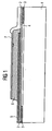
- Fig. 1 shows a piezoelectric resonant circuit produced by means of the method according to the invention.
- a carrier layer 2 which is preferably polysilicon and under which a cavity 4 in an auxiliary layer 3 z. B. is located in oxide.
- the cavity typically has the dimension of about 200 microns.
- the carrier layer 2 On the carrier layer 2 is the layer structure of the resonant circuit of a provided for the bottom electrode lower electrode layer 5, a piezoelectric layer 6 and provided for the cover electrode upper electrode layer 7.
- the electrode layers 5, 7 are preferably metal, and the piezoelectric layer 6 is z. AlN, ZnO or PZT ceramic (PbZrTi).
- This layer structure has a typical thickness of about 5 microns.
- other acoustically insulating substructures such as acoustic mirrors, may be used.
- the upper electrode layer 7 was produced with a locally adapted thickness profile. In the present example, this means that the upper electrode layer 7 formed in the region of the piezoelectric resonant circuit directly above the piezoelectric layer 6 significantly thinner than in the other areas. This was the in Fig. 1 shown thickness profile of the upper electrode layer 7 produced according to a method of the invention.
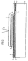
- FIGS. 2 to 4 show an embodiment of the method according to the invention using the example of in Fig. 1 shown, piezoelectric resonator.
- the starting point is the in Fig. 2 shown structure that corresponds to a piezoelectric resonant circuit without upper electrode layer 7.
- the structure shown acts as a kind of substrate for the subsequent deposition of the upper electrode layer 7.
- a relatively thick metal layer for example a tungsten layer
- a sputtering method instead of a sputtering method, a CVD method or an electrochemical method can also be used.
- the removal profile for the metal is determined. In the present example, this determination is made at the location of the resonant circuit by measuring the natural frequency of the resonant circuit. For this purpose, a needle contact 8 is guided on the metal layer and the Impendance of the resonant circuit measured as a function of the frequency of the electrical excitation ( Fig. 3 ). From the impedance curve thus obtained, the natural frequency can be determined.
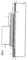
- the measured natural frequency is now compared with the desired natural frequency for the piezoelectric resonant circuit, whereby the part of the layer that has to be removed can be calculated. Since these are different thickness parts of the layer in the case of different oscillating circuits on the wafer 1 due to the thickness variations of the layer and / or due to different functions of the oscillating circuits, a specific removal profile results over the entire wafer, which is subsequently used to control the ion beam etching.
- an ion beam 9 is passed at least once over the layer, so that at the location of the ion beam, a local etching of the metal layer according to the Abtragsprofil takes place and a metal layer 7 is generated with a locally adapted to the desired natural frequency of the resonant circuit layer thickness profile ( Fig. 4 ).
- a locally controllable removal can be realized. If the wafer is scanned in tracks, then either the beam current or the scan speed can be controlled according to the locally required removal.
- the scanning takes place in any order from tracks in the x and y directions (alternatively, concentric rings or spirals are also possible) whose track pitch is significantly smaller than the half-width of the ion beam.
- the choice of the beam diameter is made according to the largest required Abtragsgradienten; Small beam diameters allow for steeper gradients, but result in globally lower volume removal per unit time.
- the control data for the translation table and the source control are obtained from an inverse convolution of the desired Abtragsprofils with the so-called "etching footprint" of the ion beam.
- an ion beam with a Gaussian current density distribution instead of an ion beam with a Gaussian current density distribution, an ion beam with a homogeneous current density distribution can also be used.
- the track pitch should be smaller than the extension of the ion beam.
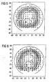
- Fig. 5 shows a typical Abtragsprofil a predominantly rotationally symmetric center-to-edge error in the thickness of a metal layer, as it can be calculated from an electrical frequency measurement at about 150 wafer positions, equivalent to 150 piezoelectric resonant circuits.
- Fig. 6 shows the corresponding measured removal profile of an ion beam etching with a gaussian Ar ion beam (half-value diameter between 5 and 50 mm), which was achieved with a speed control in the x-direction. The track pitch in the y direction was about 10% of the half-value diameter. The remaining error was in the range between 1 and 20 nm.
- the inventive method has the advantage that a frequency adjustment can be performed at wafer level and that the natural frequencies of piezoelectric resonant circuits over a large trim range of up to 20% and a frequency accuracy of 0.25% set can be.
- a layer has been produced with a layer thickness profile adapted locally to the desired natural frequency of the oscillating circuits.
- the adaptation of the layer thickness profile does not necessarily have to take place in view of the natural frequency of a resonant circuit.
- a plurality of resistors and / or capacitors with different impedance values but equal lateral Dimensions are generated.
- the method according to the invention is then used to produce a layer thickness profile adapted locally to the respective resistor or capacitor.
- a multiplicity of membranes with different mechanical parameters but the same lateral dimensions can be produced with the method according to the invention.
- the method according to the invention is then used to produce a layer thickness profile of the membrane material adapted to the respective membrane.
- FIGS. 7 to 8 show a further embodiment of the method according to the invention.
- a relatively thick layer 11 is produced on a substrate 10.
- the substrate 10 may be an insulating layer, such as an oxide layer
- the layer 11 may be a conductive layer, such as a metal layer.
- Such a choice of materials would be suitable, for example, for the generation of resistors with predetermined, different resistance values. If, on the other hand, capacitors with predetermined, different impedance values are to be produced, a conductive layer, for example a metal layer, and as layer 11 an insulating layer, for example an oxide layer, would be selected as substrate 10.
- the removal profile for the layer 11 is determined.
- the Abtragsprofil can be determined for example with a resistance measurement.
- interferometric measurements can also be used.
- the present example assumes that distributed over the wafer resistors with two different Resistance values are to be generated. Therefore, a lacquer layer is then applied and developed, so that a resist mask 12 is formed, which is open at the points at which the resistors 13 are to be generated with a first resistance value. Subsequently, an ion beam etching takes place, which performs an etching in accordance with the predetermined removal profile with an ion beam 9 at the open locations of the resist mask 12. All other areas of the layer 11 are protected by the resist mask 12 ( Fig. 7 ).
- the resist mask 12 is removed and another resist layer is applied and developed to form another resist mask 14 which is opened at the locations where the resistors 15 are to be formed with a second resistance.
- an ion beam etching is again carried out, which performs an etching in accordance with the predetermined removal profile at the open locations of the resist mask 14. All other areas of the layer 11 are protected by the resist mask 14 ( Fig. 8 ). After the removal of the resist mask 14, one thus obtains a layer 11 with a layer thickness profile locally adapted to the respective resistance.
Landscapes
- Chemical & Material Sciences (AREA)
- Engineering & Computer Science (AREA)
- Metallurgy (AREA)
- Organic Chemistry (AREA)
- Materials Engineering (AREA)
- Mechanical Engineering (AREA)
- Chemical Kinetics & Catalysis (AREA)
- Manufacturing & Machinery (AREA)
- Physics & Mathematics (AREA)
- Plasma & Fusion (AREA)
- Microelectronics & Electronic Packaging (AREA)
- General Chemical & Material Sciences (AREA)
- Analytical Chemistry (AREA)
- Drying Of Semiconductors (AREA)
- Piezo-Electric Or Mechanical Vibrators, Or Delay Or Filter Circuits (AREA)
- Powder Metallurgy (AREA)
Priority Applications (1)
| Application Number | Priority Date | Filing Date | Title |
|---|---|---|---|
| DE50114591T DE50114591D1 (de) | 2001-05-22 | 2001-05-22 | Verfahren zur Herstellung einer Schicht mit einem vorgegebenen Schichtdickenprofil |
Applications Claiming Priority (2)
| Application Number | Priority Date | Filing Date | Title |
|---|---|---|---|
| EP01962685A EP1390559B1 (de) | 2001-05-22 | 2001-05-22 | Verfahren zur herstellung einer schicht mit einem vordefinierten schichtdickenprofil |
| PCT/EP2001/005889 WO2002095085A1 (de) | 2001-05-22 | 2001-05-22 | Frequenzabgleich für bulk-acoustic-wave resonatoren durch lokales ionenstrahlätzen |
Related Parent Applications (1)
| Application Number | Title | Priority Date | Filing Date |
|---|---|---|---|
| EP01962685A Division EP1390559B1 (de) | 2001-05-22 | 2001-05-22 | Verfahren zur herstellung einer schicht mit einem vordefinierten schichtdickenprofil |
Publications (3)
| Publication Number | Publication Date |
|---|---|
| EP1816233A2 EP1816233A2 (de) | 2007-08-08 |
| EP1816233A3 EP1816233A3 (de) | 2007-08-22 |
| EP1816233B1 true EP1816233B1 (de) | 2008-12-17 |
Family
ID=8164429
Family Applications (2)
| Application Number | Title | Priority Date | Filing Date |
|---|---|---|---|
| EP07008531A Expired - Lifetime EP1816233B1 (de) | 2001-05-22 | 2001-05-22 | Verfahren zur Herstellung einer Schicht mit einem vorgegebenen Schichtdickenprofil |
| EP01962685A Expired - Lifetime EP1390559B1 (de) | 2001-05-22 | 2001-05-22 | Verfahren zur herstellung einer schicht mit einem vordefinierten schichtdickenprofil |
Family Applications After (1)
| Application Number | Title | Priority Date | Filing Date |
|---|---|---|---|
| EP01962685A Expired - Lifetime EP1390559B1 (de) | 2001-05-22 | 2001-05-22 | Verfahren zur herstellung einer schicht mit einem vordefinierten schichtdickenprofil |
Country Status (6)
| Country | Link |
|---|---|
| US (1) | US20040212459A1 (enExample) |
| EP (2) | EP1816233B1 (enExample) |
| JP (1) | JP2004527972A (enExample) |
| KR (1) | KR20040005977A (enExample) |
| DE (2) | DE50112976D1 (enExample) |
| WO (1) | WO2002095085A1 (enExample) |
Families Citing this family (6)
| Publication number | Priority date | Publication date | Assignee | Title |
|---|---|---|---|---|
| DE102004054895B4 (de) * | 2004-11-12 | 2007-04-19 | Infineon Technologies Ag | Dünnschicht-BAW-Filter sowie Verfahren zur Herstellung eines Dünnschicht-BAW-Filters |
| JP2008098528A (ja) * | 2006-10-13 | 2008-04-24 | Toshiba Corp | 半導体装置の製造方法 |
| US7535324B2 (en) * | 2007-06-15 | 2009-05-19 | Avago Technologies Wireless Ip, Pte. Ltd. | Piezoelectric resonator structure and method for manufacturing a coupled resonator device |
| FR2941878B1 (fr) * | 2009-02-10 | 2011-05-06 | Quertech Ingenierie | Procede de traitement par un faisceau d'ions d'une couche metallique deposee sur un substrat |
| US8479363B2 (en) * | 2010-05-11 | 2013-07-09 | Hao Zhang | Methods for wafer level trimming of acoustically coupled resonator filter |
| JP6719178B2 (ja) * | 2015-05-22 | 2020-07-08 | エスアイアイ・クリスタルテクノロジー株式会社 | 圧電振動片の製造方法及び圧電振動子の製造方法 |
Family Cites Families (20)
| Publication number | Priority date | Publication date | Assignee | Title |
|---|---|---|---|---|
| US2877338A (en) * | 1954-10-22 | 1959-03-10 | James Knights Company | Method of adjusting the operating frequency of sealed piezoelectric crystals |
| US3699334A (en) * | 1969-06-16 | 1972-10-17 | Kollsman Instr Corp | Apparatus using a beam of positive ions for controlled erosion of surfaces |
| FR2354617A1 (fr) * | 1976-06-08 | 1978-01-06 | Electro Resistance | Procede pour la fabrication de resistances electriques a partir de feuilles ou de films metalliques et resistances obtenues |
| JPS58106750A (ja) * | 1981-12-18 | 1983-06-25 | Toshiba Corp | フオ−カスイオンビ−ム加工方法 |
| JPS6042832A (ja) * | 1983-08-18 | 1985-03-07 | Matsushita Electric Ind Co Ltd | イオンビ−ム装置 |
| JPS61137327A (ja) * | 1984-12-10 | 1986-06-25 | Nec Corp | 層間絶縁膜のエツチング方法 |
| EP0203573B1 (en) * | 1985-05-28 | 1993-08-11 | Rikagaku Kenkyusho | Electron beam-excited ion beam source |
| JP2713923B2 (ja) * | 1987-10-07 | 1998-02-16 | 株式会社日立製作所 | 集束イオンビームを用いたデバイス加工方法 |
| JPH04196610A (ja) * | 1990-11-26 | 1992-07-16 | Seiko Epson Corp | 圧電振動子の周波数調整方法 |
| US5266529A (en) * | 1991-10-21 | 1993-11-30 | Trw Inc. | Focused ion beam for thin film resistor trim on aluminum nitride substrates |
| JPH0773834A (ja) * | 1993-08-31 | 1995-03-17 | Nippon Steel Corp | 透過電子顕微鏡用薄膜試料作製方法 |
| US5876860A (en) * | 1997-12-09 | 1999-03-02 | N.V. Interturbine | Thermal barrier coating ceramic structure |
| JP3473538B2 (ja) * | 1999-05-14 | 2003-12-08 | 株式会社村田製作所 | 圧電部品の周波数調整装置及び周波数調整方法 |
| US6529311B1 (en) * | 1999-10-28 | 2003-03-04 | The Trustees Of Boston University | MEMS-based spatial-light modulator with integrated electronics |
| US6307447B1 (en) * | 1999-11-01 | 2001-10-23 | Agere Systems Guardian Corp. | Tuning mechanical resonators for electrical filter |
| US6537606B2 (en) * | 2000-07-10 | 2003-03-25 | Epion Corporation | System and method for improving thin films by gas cluster ion beam processing |
| US6456173B1 (en) * | 2001-02-15 | 2002-09-24 | Nokia Mobile Phones Ltd. | Method and system for wafer-level tuning of bulk acoustic wave resonators and filters |
| US6456011B1 (en) * | 2001-02-23 | 2002-09-24 | Front Range Fakel, Inc. | Magnetic field for small closed-drift ion source |
| US6874211B2 (en) * | 2001-03-05 | 2005-04-05 | Agilent Technologies, Inc. | Method for producing thin film bulk acoustic resonators (FBARs) with different frequencies on the same substrate by subtracting method and apparatus embodying the method |
| US6441702B1 (en) * | 2001-04-27 | 2002-08-27 | Nokia Mobile Phones Ltd. | Method and system for wafer-level tuning of bulk acoustic wave resonators and filters |
-
2001
- 2001-05-22 DE DE50112976T patent/DE50112976D1/de not_active Expired - Lifetime
- 2001-05-22 KR KR10-2003-7015186A patent/KR20040005977A/ko not_active Ceased
- 2001-05-22 EP EP07008531A patent/EP1816233B1/de not_active Expired - Lifetime
- 2001-05-22 WO PCT/EP2001/005889 patent/WO2002095085A1/de not_active Ceased
- 2001-05-22 DE DE50114591T patent/DE50114591D1/de not_active Expired - Lifetime
- 2001-05-22 EP EP01962685A patent/EP1390559B1/de not_active Expired - Lifetime
- 2001-05-22 JP JP2002591547A patent/JP2004527972A/ja active Pending
- 2001-05-22 US US10/478,751 patent/US20040212459A1/en not_active Abandoned
Also Published As
| Publication number | Publication date |
|---|---|
| DE50114591D1 (de) | 2009-01-29 |
| EP1390559B1 (de) | 2007-09-05 |
| EP1816233A3 (de) | 2007-08-22 |
| DE50112976D1 (de) | 2007-10-18 |
| US20040212459A1 (en) | 2004-10-28 |
| JP2004527972A (ja) | 2004-09-09 |
| KR20040005977A (ko) | 2004-01-16 |
| WO2002095085A1 (de) | 2002-11-28 |
| WO2002095085A8 (de) | 2002-12-19 |
| EP1816233A2 (de) | 2007-08-08 |
| EP1390559A1 (de) | 2004-02-25 |
Similar Documents
| Publication | Publication Date | Title |
|---|---|---|
| EP1393440B1 (de) | Piezoelektrische resonatorvorrichtung mit verstimmungsschichtfolge | |
| DE10330136B4 (de) | Film Bulk Acoustic Resonator (FBAR) und Verfahren zu seiner Herstellung | |
| DE10207342B4 (de) | Verfahren zum Liefern unterschiedlicher Frequenzeinstellungen bei einem akustischen Dünnfilmvolumenresonator- (FBAR-) Filter und Vorrichtung, die das Verfahren beinhaltet | |
| DE10207341B4 (de) | Verfahren zum Erzeugen akustischer Dünnfilmvolumenresonatoren (FBARs) mit unterschiedlichen Frequenzen auf einem einzelnen Substrat und Vorrichtung, die das Verfahren beinhaltet | |
| DE10207330B4 (de) | Verfahren zum Herstellen akustischer Dünnfilmvolumenresonatoren (FBARs) mit unterschiedlichen Frequenzen auf dem gleichen Substrat durch ein Subtraktionsverfahren und Vorrichtung, die das Verfahren beinhaltet | |
| DE3340563C2 (de) | Schichtkondensator und Verfahren zur Herstellung desselben | |
| DE112017000522B4 (de) | Chip-Widerstand und Verfahren für die Herstellung desselben | |
| EP1464113B1 (de) | Verfahren zur herstellung einer topologieoptimierten elektrode für einen resonator in dünnfilmtechnologie | |
| DE3043289A1 (de) | Herstellungverfahren fuer eine halbleitereinrichtung | |
| EP1816233B1 (de) | Verfahren zur Herstellung einer Schicht mit einem vorgegebenen Schichtdickenprofil | |
| DE68919808T2 (de) | Herstellungsverfahren für akustische Oberflächenwellenanordnungen und auf diese Weise hergestellte akustische Oberflächenwellenanordnungen. | |
| EP1456947B1 (de) | Piezoelektrischer schwingkreis, verfahren zu dessen herstellung und filteranordnung | |
| DE102008016613B4 (de) | Verfahren zur Herstellung eines elektrischen Bauelements mit mindestens einer dielektrischen Schicht und ein elektrisches Bauelement mit mindestens einer dielektrischen Schicht | |
| DE102009019523B4 (de) | Verfahren zum Trimmen eines SAW Bauelements | |
| JP2004527972A5 (enExample) | ||
| DE102019130514B4 (de) | Trimmverfahren für einen SAW-Wafer, getrimmte Wafer und getrimmte SAW-Vorrichtungen | |
| DE69427208T2 (de) | Planar-Induktivität mit operativer Kalibrierung in einem RF-System | |
| DE10162540A1 (de) | Bauelement und Verfahren zu dessen Herstellung | |
| EP0660411A2 (de) | Integrierte Halbleiterschaltung mit Kondensatoren genau definierter Kapazität | |
| DE19940560C2 (de) | Verfahren zur Herstellung eines Halbleiterchips mit nach dem Siliziumprozess einstellbarer elektrischer Eigenschaft | |
| DE102022130335A1 (de) | Verbesserter nickel-chrom-aluminium-dünnfilmwiderstand | |
| DD278902A1 (de) | Verfahren zum frequenzabgleich vnn akustischen oberflaechenwellen-resonatoren | |
| DE102019121781A1 (de) | Verfahren zur Herstellung einer interdigitalen Elektrodenstruktur und elektrisches Bauelement | |
| DE4434090A1 (de) | Verfahren zur Ausbildung feiner Muster in Halbleitervorrichtungen | |
| DD147422A5 (de) | Verfahren und schaltungsanordnung zur reflexions-und daempfungsmessung an daempfungsgliedern |
Legal Events
| Date | Code | Title | Description |
|---|---|---|---|
| PUAI | Public reference made under article 153(3) epc to a published international application that has entered the european phase |
Free format text: ORIGINAL CODE: 0009012 |
|
| PUAL | Search report despatched |
Free format text: ORIGINAL CODE: 0009013 |
|
| 17P | Request for examination filed |
Effective date: 20070426 |
|
| AC | Divisional application: reference to earlier application |
Ref document number: 1390559 Country of ref document: EP Kind code of ref document: P |
|
| AK | Designated contracting states |
Kind code of ref document: A2 Designated state(s): DE FR GB IT NL |
|
| AK | Designated contracting states |
Kind code of ref document: A3 Designated state(s): DE FR GB IT NL |
|
| RIN1 | Information on inventor provided before grant (corrected) |
Inventor name: ELBRECHT, LUEDER Inventor name: MARKSTEINER, STEPHAN Inventor name: AIGNER, ROBERT Inventor name: NESSLER, WINFRIED Inventor name: TIMME, HANS-JOERG |
|
| 17Q | First examination report despatched |
Effective date: 20071119 |
|
| AKX | Designation fees paid |
Designated state(s): DE FR GB IT NL |
|
| GRAP | Despatch of communication of intention to grant a patent |
Free format text: ORIGINAL CODE: EPIDOSNIGR1 |
|
| GRAS | Grant fee paid |
Free format text: ORIGINAL CODE: EPIDOSNIGR3 |
|
| GRAS | Grant fee paid |
Free format text: ORIGINAL CODE: EPIDOSNIGR3 |
|
| GRAA | (expected) grant |
Free format text: ORIGINAL CODE: 0009210 |
|
| AC | Divisional application: reference to earlier application |
Ref document number: 1390559 Country of ref document: EP Kind code of ref document: P |
|
| AK | Designated contracting states |
Kind code of ref document: B1 Designated state(s): DE FR GB IT NL |
|
| REG | Reference to a national code |
Ref country code: GB Ref legal event code: FG4D Free format text: NOT ENGLISH |
|
| REF | Corresponds to: |
Ref document number: 50114591 Country of ref document: DE Date of ref document: 20090129 Kind code of ref document: P |
|
| RAP2 | Party data changed (patent owner data changed or rights of a patent transferred) |
Owner name: AVAGO TECHNOLOGIES WIRELESS IP (SINGAPORE) PTE. LT |
|
| NLT2 | Nl: modifications (of names), taken from the european patent patent bulletin |
Owner name: AVAGO TECHNOLOGIES WIRELESS IP Effective date: 20090318 |
|
| PG25 | Lapsed in a contracting state [announced via postgrant information from national office to epo] |
Ref country code: NL Free format text: LAPSE BECAUSE OF FAILURE TO SUBMIT A TRANSLATION OF THE DESCRIPTION OR TO PAY THE FEE WITHIN THE PRESCRIBED TIME-LIMIT Effective date: 20081217 |
|
| NLV1 | Nl: lapsed or annulled due to failure to fulfill the requirements of art. 29p and 29m of the patents act | ||
| PLBE | No opposition filed within time limit |
Free format text: ORIGINAL CODE: 0009261 |
|
| STAA | Information on the status of an ep patent application or granted ep patent |
Free format text: STATUS: NO OPPOSITION FILED WITHIN TIME LIMIT |
|
| 26N | No opposition filed |
Effective date: 20090918 |
|
| GBPC | Gb: european patent ceased through non-payment of renewal fee |
Effective date: 20090522 |
|
| REG | Reference to a national code |
Ref country code: FR Ref legal event code: ST Effective date: 20100129 |
|
| PG25 | Lapsed in a contracting state [announced via postgrant information from national office to epo] |
Ref country code: FR Free format text: LAPSE BECAUSE OF NON-PAYMENT OF DUE FEES Effective date: 20090602 |
|
| PG25 | Lapsed in a contracting state [announced via postgrant information from national office to epo] |
Ref country code: GB Free format text: LAPSE BECAUSE OF NON-PAYMENT OF DUE FEES Effective date: 20090522 |
|
| PG25 | Lapsed in a contracting state [announced via postgrant information from national office to epo] |
Ref country code: IT Free format text: LAPSE BECAUSE OF FAILURE TO SUBMIT A TRANSLATION OF THE DESCRIPTION OR TO PAY THE FEE WITHIN THE PRESCRIBED TIME-LIMIT Effective date: 20081217 |
|
| PGFP | Annual fee paid to national office [announced via postgrant information from national office to epo] |
Ref country code: DE Payment date: 20110518 Year of fee payment: 11 |
|
| REG | Reference to a national code |
Ref country code: DE Ref legal event code: R119 Ref document number: 50114591 Country of ref document: DE Effective date: 20121201 |
|
| PG25 | Lapsed in a contracting state [announced via postgrant information from national office to epo] |
Ref country code: DE Free format text: LAPSE BECAUSE OF NON-PAYMENT OF DUE FEES Effective date: 20121201 |