EP1814232B1 - Pipelined analog-to-digital converters - Google Patents
Pipelined analog-to-digital converters Download PDFInfo
- Publication number
- EP1814232B1 EP1814232B1 EP06024141.1A EP06024141A EP1814232B1 EP 1814232 B1 EP1814232 B1 EP 1814232B1 EP 06024141 A EP06024141 A EP 06024141A EP 1814232 B1 EP1814232 B1 EP 1814232B1
- Authority
- EP
- European Patent Office
- Prior art keywords
- voltage
- analog
- digital
- integrated circuit
- adc stage
- Prior art date
- Legal status (The legal status is an assumption and is not a legal conclusion. Google has not performed a legal analysis and makes no representation as to the accuracy of the status listed.)
- Ceased
Links
- 238000013500 data storage Methods 0.000 description 24
- 230000001413 cellular effect Effects 0.000 description 12
- 238000010586 diagram Methods 0.000 description 12
- 230000006870 function Effects 0.000 description 7
- 238000000034 method Methods 0.000 description 7
- 238000004364 calculation method Methods 0.000 description 6
- 230000003287 optical effect Effects 0.000 description 6
- 238000004891 communication Methods 0.000 description 2
- 230000003044 adaptive effect Effects 0.000 description 1
- 230000005540 biological transmission Effects 0.000 description 1
- 238000006243 chemical reaction Methods 0.000 description 1
- 230000001419 dependent effect Effects 0.000 description 1
- 238000012986 modification Methods 0.000 description 1
- 230000004048 modification Effects 0.000 description 1
- 238000013139 quantization Methods 0.000 description 1
- 238000005070 sampling Methods 0.000 description 1
Images


Classifications
-
- H—ELECTRICITY
- H03—ELECTRONIC CIRCUITRY
- H03M—CODING; DECODING; CODE CONVERSION IN GENERAL
- H03M1/00—Analogue/digital conversion; Digital/analogue conversion
- H03M1/12—Analogue/digital converters
- H03M1/14—Conversion in steps with each step involving the same or a different conversion means and delivering more than one bit
- H03M1/145—Conversion in steps with each step involving the same or a different conversion means and delivering more than one bit the steps being performed sequentially in series-connected stages
-
- H—ELECTRICITY
- H03—ELECTRONIC CIRCUITRY
- H03M—CODING; DECODING; CODE CONVERSION IN GENERAL
- H03M1/00—Analogue/digital conversion; Digital/analogue conversion
- H03M1/002—Provisions or arrangements for saving power, e.g. by allowing a sleep mode, using lower supply voltage for downstream stages, using multiple clock domains or by selectively turning on stages when needed
Definitions
- the present disclosure relates to pipelined analog-to-digital converters (ADCs).
- ADCs analog-to-digital converters
- ADCs Analog-to-digital converters
- the ADC may include a pipelined ADC that utilizes multiple stages. Each stage employs a sample and hold circuit that samples an analog Input voltage V in to the pipelined ADC or a residue voltage V res from a prior stage. In addition, each of the stages receives a reference voltage V ref .
- the ADC 10 includes a plurality of stages 12-1, 12-2, and 12-3 (collectively stages 12) that are cascaded in series. Although three stages 12-1, 12-2, and 12-3 are shown, the pipelined ADC 10 may include additional or fewer stages.
- Some of the A/D converter stages 12 include a sample and hold module 14 that samples and holds the analog input signal V in or the residue signal V res from a prior stage.
- a low resolution A/D subconverter module 16 quantizes the held analog signal to a resolution of B i bits where / corresponds to the current stage of the pipelined A/D converter 10.
- the number of bits per stage B, and/or the number of stages may be determined in part by the desired sampling rate and resolution.
- the output of the A/D subconverter module 16 is supplied to a low-resolution D/A subconverter module 18 that converts the resulting digital output signal back into an analog representation.
- the D/A subconverter module 18 may have a resolution that is equivalent to that of the corresponding A/D subconverter module 16 of the same stage.
- a difference module 20 subtracts the analog output from the D/A subconverter module 18 from the voltage input V in to generate a residue signal V res .
- the residue signal V res is equal to the difference between the held analog signal (V in or V res from the prior stage) and the reconstructed analog signal.
- An analog interstage difference module 22 may be used to amplify the residue signal.
- the amplified residue signal is output to the next stage 12-2 of the pipelined ADC 10.
- the first ADC stage 12-1 of the pipelined ADC 10 operates on a most current analog input sample while the second ADC stage 12-2 operates on the amplified residue of the prior input sample.
- the third stage 12-3 operates on the amplified residue output by the second ADC stage 12-2.
- US 5 394 148 discloses a ADC that includes a first stage and a second stage. The first generates a first reference voltage via a first resistor string. The second stage generates a second reference voltage via a second resistor string. This object is solved by the invention as claimed in the independent claim. Preferred embodiments of the invention are defined by the dependent claims.
- FIG. 1 is a functional block diagram of a pipelined analog to digital converter (ADC) according to the prior art
- FIG. 2 is a functional block diagram of an exemplary pipelined ADC according to the present invention.
- FIG. 3 is a functional block diagram of another exemplary pipelined ADC according to the present invention.
- FIG. 4 is a functional block diagram of an integrated circuit including a pipelined ADC according to the present invention.
- FIG. 5 is a functional block diagram of an integrated circuit including an analog voltage supply, a digital voltage supply, and a pipelined ADC according to the present invention
- FIG. 6A is a functional block diagram of a hard disk drive
- FIG. 6B is a functional block diagram of a digital versatile disk (DVD).
- DVD digital versatile disk
- FIG. 6C is a functional block diagram of a high definition television
- FIG. 6D is a functional block diagram of a vehicle control system
- FIG. 6E is a functional block diagram of a cellular phone
- FIG. 6F is a functional block diagram of a set top box.
- FIG. 6G is a functional block diagram of a media player.
- module, circuit and/or device refers to an Application Specific Integrated Circuit (ASIC), an electronic circuit, a processor (shared, dedicated, or group) and memory that execute one or more software or firmware programs, a combinational logic circuit, and/or other suitable components that provide the described functionality.
- ASIC Application Specific Integrated Circuit
- processor shared, dedicated, or group
- memory that execute one or more software or firmware programs, a combinational logic circuit, and/or other suitable components that provide the described functionality.
- phrase at least one of A, B, and C should be construed to mean a logical (A or B or C), using a non-exclusive logical or. It should be understood that steps within a method may be executed In different order without altering the principles of the present disclosure.
- a pipelined ADC 100 including multiple voltage references V ref_l is shown, where / corresponds to the current stage of the pipelined ADC 100.
- the pipelined ADC 100 includes stages 112-1, 112-2, and 112-3 (collectively stages 112), a sample and hold module 114, an ADC module 116, a digital to analog converter (DAC) module 118, a difference module 120 and an amplifier module 122. While three stages are shown, additional or fewer stages can be used.
- the quantization of bits by a subsequent stage of the pipelined ADC 100 does not require the same signal to noise levels (SNR) as the current stage and therefore a lower reference voltage can be used for at least one of the second and third stages.
- SNR signal to noise levels
- the power consumed by stages 112-1, 112-2, and 112-3 of the pipelined ADC 100 is related to the voltage reference of each stage. As a result, the pipelined ADC 100 tends to consume less power than a pipelined ADC having stages supplied with the same voltage reference as shown in FIG. 1 .
- V ref_l a pipelined ADC 110 including different voltage references, V ref_l is shown, where l corresponds to the current stage of the pipelined A/D converter 110. At least one of the voltage references V ref_l is derived from an analog supply voltage V analog_ref for analog circuits in the system containing the ADC 110 and at least one of the voltage references is derived from a digital supply voltage V digital_ref for digital circuit In the system containing the ADC 110.
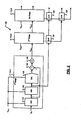
- an integrated circuit (IC) 200 is shown.
- One or more power supply 202 supplies unregulated voltage to voltage regulators 204 and 206.
- a first voltage regulator 204 provides analog supply voltages, V analog_ref_1 , V analog_ref_2 , ..., and V analog_ref_X , where X is an integer greater than zero.
- a second voltage regulator 206 provides digital supply voltages, V digital_ref_1 , V digital_ref_2 , ..., and V digital_ref_Y , where Y is an Integer greater than zero.
- the IC 200 may also include IC components 210 to perform additional circuit functions.
- the first voltage regulator 204 also supplies one or more analog circuits 216 In the IC 200.
- the second voltage regulator 206 also supplies one or more digital circuits 214.
- An integrated circuit (IC) 220 is shown.
- An analog voltage supply 224 generates analog supply voltages, V analog_ref_1 , V analog_ref_2 , ..., and V analog_ref_X , where X is an integer greater than zero.
- a digital voltage supply 226 generates digital supply voltages, V digital_ref_1 , V digital_ref_2 , ..., and V digital_ref_Y , where Y is an integer greater than zero.
- the IC 220 may also include IC components 210 to perform additional circuit functions.
- the analog voltage supply 224 also supplies one or more analog circuits 216 in the IC 200.
- the digital voltage supply 226 also supplies one or more digital circuits 214.
- the device can be implemented in one of more ADCs in a hard disk drive 400.
- the device may implement and/or be implemented in either or both signal processing and/or control circuits, which are generally identified in FIG. 6A at 402 and/or in a power supply 403.
- the signal processing and/or control circuit 402 and/or other circuits (not shown) in the HDD 400 may process data, perform coding and/or encryption, perform calculations, and/or format data that is output to and/or received from a magnetic storage medium 406.
- the HDD 400 may communicate with a host device (not shown) such as a computer, mobile computing devices such as personal digital assistants, cellular phones, media or MP3 players and the like, and/or other devices via one or more wired or wireless communication links 408.
- a host device such as a computer, mobile computing devices such as personal digital assistants, cellular phones, media or MP3 players and the like, and/or other devices via one or more wired or wireless communication links 408.
- the HDD 400 may be connected to memory 409 such as random access memory (RAM).
- RAM random access memory
- ROM read only memory
- the device can be implemented in one of more ADCs in a digital versatile disc (DVD) drive 410.
- the device may implement and/or be implemented In either or both signal processing and/or control circuits, which are generally identified In FIG. 6B at 412, mass data storage of the DVD drive 410 and/or a power supply 413.
- the signal processing and/or control circuit 412 and/or other circuits (not shown) In the DVD 410 may process data, perform coding and/or encryption, perform calculations, and/or format data that is read from and/or data written to an optical storage medium 416.
- the signal processing and/or control circuit 412 and/or other circuits (not shown) in the DVD 410 can also perform other functions such as encoding and/or decoding and/or any other signal processing functions associated with a DVD drive.
- the DVD drive 410 may communicate with an output device (not shown) such as a computer, television or other device via one or more wired or wireless communication links 417.
- the DVD 410 may communicate with mass data storage 418 that stores data in a nonvolatile manner.
- the mass data storage 418 may include a hard disk drive (HDD).
- the HDD may have the configuration shown in FIG. 6A .
- the HDD may be a mini HDD that includes one or more platters having a diameter that is smaller than approximately 1.8".
- the DVD 410 may be connected to memory 419 such as RAM, ROM, low latency nonvolatile memory such as flash memory and/or other suitable electronic data storage.
- the device can be implemented in one of more ADCs in a high definition television (HDTV) 420.
- the device may implement and/or be implemented In either or both signal processing and/or control circuits, which are generally identified in FIG. 6E at 422, a WLAN interface, mass data storage of the HDTV 420 and/or a power supply 423.
- the HDTV 420 receives HDTV input signals in either a wired or wireless format and generates HDTV output signals for a display 426.
- signal processing circuit and/or control circuit 422 and/or other circuits (not shown) of the HDTV 420 may process data, perform coding and/or encryption, perform calculations, format data and/or perform any other type of HDTV processing that may be required.
- the HDTV 420 may communicate with mass data storage 427 that stores data in a nonvolatile manner such as optical and/or magnetic storage devices. At least one HDD may have the configuration shown in FIG. 6A and/or at least one DVD may have the configuration shown in FIG. 6B .
- the HDD may be a mini HDD that includes one or more platters having a diameter that is smaller than approximately 1,8".
- the HDTV 420 may be connected to memory 428 such as RAM, ROM, low latency nonvolatile memory such as flash memory and/or other suitable electronic data storage.
- the HDTV 420 also may support connections with a WLAN via a WLAN network interface 429.
- the device may implement and/or be implemented in one of more ADCs in a control system of a vehicle 430, a WLAN interface, mass data storage of the vehicle control system and/or a power supply 433.
- the device implement a powertrain control system 432 that receives Inputs from one or more sensors such as temperature sensors, pressure sensors, rotational sensors, airflow sensors and/or any other suitable sensors and/or that generates one or more output control signals such as engine operating parameters, transmission operating parameters, and/or other control signals.
- the device may also be implemented in other control systems 440 of the vehicle 430.
- the control system 440 may likewise receive signals from input sensors 442 and/or output control signals to one or more output devices 444.
- the control system 440 may be part of an anti-lock braking system (ABS), a navigation system, a telematics system, a vehicle telematics system, a lane departure system, an adaptive cruise control system, a vehicle entertainment system such as a stereo, DVD, compact disc and the like. Still other implementations are contemplated.
- the powertrain control system 432 may communicate with mass data storage 446 that stores data in a nonvolatile manner.
- the mass data storage 446 may include optical and/or magnetic storage devices for example hard disk drives HDD and/or DVDs. At least one HDD may have the configuration shown in FIG. 6A and/or at least one DVD may have the configuration shown in FIG. 6B .
- the HDD may be a mini HDD that includes one or more platters having a diameter that is smaller than approximately 1.8".
- the powertrain control system 432 may be connected to memory 447 such as RAM, ROM, low latency nonvolatile memory such as flash memory and/or other suitable electronic data storage.
- the powertrain control system 432 also may support connections with a WLAN via a WLAN network Interface 448.
- the control system 440 may also include mass data storage, memory and/or a WLAN interface (all not shown).
- the device can be implemented in one of more ADCs In a cellular phone 450 that may include a cellular antenna 451.
- the device may implement and/or be implemented in either or both signal processing and/or control circuits, which are generally identified in FIG. 6E at 452, a WLAN interface, mass data storage of the cellular phone 450 and/or a power supply 453.
- the cellular phone 450 includes a microphone 456, an audio output 458 such as a speaker and/or audio output jack, a display 460 and/or an input device 462 such as a keypad, pointing device, voice actuation and/or other input device.
- the signal processing and/or control circuits 452 and/or other circuits (not shown) in the cellular phone 450 may process data, perform coding and/or encryption, perform calculations, format data and/or perform other cellular phone functions.
- the cellular phone 450 may communicate with mass data storage 464 that stores data in a nonvolatile manner such as optical and/or magnetic storage devices for example hard disk drives HDD and/or DVDs. At least one HDD may have the configuration shown in FIG. 6A and/or at least one DVD may have the configuration shown in FIG. 6B .
- the HDD may be a mini HDD that includes one or more platters having a diameter that Is smaller than approximately 1.8".
- the cellular phone 450 may be connected to memory 466 such as RAM, ROM, low latency nonvolatile memory such as flash memory and/or other suitable electronic data storage.
- the cellular phone 450 also may support connections with a WLAN via a WLAN network interface 468.
- the device can be implemented in one of more ADCs in a set top box 480.
- the device may implement and/or be Implemented in either or both signal processing and/or control circuits, which are generally identified in FIG. 6F at 484, a WLAN interface, mass data storage of the set top box 480 and/or a power supply 483.
- the set top box 480 receives signals from a source such as a broadband source and outputs standard and/or high definition audio/video signals suitable for a display 488 such as a television and/or monitor and/or other video and/or audio output devices.
- the signal processing and/or control circuits 484 and/or other circuits (not shown) of the set top box 480 may process data, perform coding and/or encryption, perform calculations, format data and/or perform any other set top box function.
- the set top box 480 may communicate with mass data storage 490 that stores data in a nonvolatile manner.
- the mass data storage 490 may include optical and/or magnetic storage devices for example hard disk drives HDD and/or DVDs. At least one HDD may have the configuration shown in FIG. 6A and/or at least one DVD may have the configuration shown in FIG. 6B .
- the HDD may be a mini HDD that includes one or more platters having a diameter that is smaller than approximately 1.8".
- the set top box 480 may be connected to memory 494 such as RAM, ROM, low latency nonvolatile memory such as flash memory and/or other suitable electronic data storage.
- the set top box 480 also may support connections with a WLAN via a WLAN network interface 496.
- the device can be Implemented In one of more ADCs in a media player 500.
- the device may implement and/or be implemented in either or both signal processing and/or control circuits, which are generally identified in FIG. 6G at 504, a WLAN interface, mass data storage of the media player 500 and/or a power supply 503.
- the media player 500 includes a display 507 and/or a user input 508 such as a keypad, touchpad and the like.
- the media player 500 may employ a graphical user Interface (GUI) that typically employs menus, drop down menus, icons and/or a point-and-click Interface via the display 507 and/or user input 508.
- GUI graphical user Interface
- the media player 500 further includes an audio output 509 such as a speaker and/or audio output Jack.
- the signal processing and/or control circuits 504 and/or other circuits (not shown) of the media player 500 may process data, perform coding and/or encryption, perform calculations, format data and/or perform any other media player function.
- the media player 500 may communicate with mass data storage 510 that stores data such as compressed audio and/or video content in a nonvolatile manner.
- the compressed audio files include files that are compliant with MP3 format or other suitable compressed audio and/or video formats.
- the mass data storage may include optical and/or magnetic storage devices for example hard disk drives HDD and/or DVDs. At least one HDD may have the configuration shown in FIG. 6A and/or at least one DVD may have the configuration shown in FIG. 6B .
- the HDD may be a mini HDD that includes one or more platters having a diameter that is smaller than approximately 1.8".
- the media player 500 may be connected to memory 514 such as RAM, ROM, low latency nonvolatile memory such as flash memory and/or other suitable electronic data storage.
- the media player 500 also may support connections with a WLAN via a WLAN network interface 516. Still other implementations in addition to those described above are contemplated.
Landscapes
- Engineering & Computer Science (AREA)
- Theoretical Computer Science (AREA)
- Analogue/Digital Conversion (AREA)
- Signal Processing For Digital Recording And Reproducing (AREA)
- Navigation (AREA)
Applications Claiming Priority (1)
| Application Number | Priority Date | Filing Date | Title |
|---|---|---|---|
| US11/333,935 US7541962B2 (en) | 2006-01-18 | 2006-01-18 | Pipelined analog-to-digital converters |
Publications (2)
| Publication Number | Publication Date |
|---|---|
| EP1814232A1 EP1814232A1 (en) | 2007-08-01 |
| EP1814232B1 true EP1814232B1 (en) | 2013-05-15 |
Family
ID=37685987
Family Applications (1)
| Application Number | Title | Priority Date | Filing Date |
|---|---|---|---|
| EP06024141.1A Ceased EP1814232B1 (en) | 2006-01-18 | 2006-11-21 | Pipelined analog-to-digital converters |
Country Status (6)
| Country | Link |
|---|---|
| US (2) | US7541962B2 (enExample) |
| EP (1) | EP1814232B1 (enExample) |
| JP (1) | JP4939201B2 (enExample) |
| CN (1) | CN101005283B (enExample) |
| SG (1) | SG134212A1 (enExample) |
| TW (1) | TWI420827B (enExample) |
Families Citing this family (8)
| Publication number | Priority date | Publication date | Assignee | Title |
|---|---|---|---|---|
| US7830287B1 (en) * | 2009-05-08 | 2010-11-09 | Himax Media Solutions, Inc. | Analog to digital converter having digital correction logic that utilizes a dither signal to correct a digital code |
| CN101777917B (zh) * | 2010-01-14 | 2013-04-03 | 上海迦美信芯通讯技术有限公司 | 一种流水线模数转换器及其电容失配的快速校准方法 |
| KR101381250B1 (ko) * | 2010-09-15 | 2014-04-04 | 한국전자통신연구원 | 아날로그 디지털 변환 장치 및 그것의 기준 전압 제어 방법 |
| CN103247321A (zh) * | 2012-02-01 | 2013-08-14 | 宸定股份有限公司 | 应用3.5英寸硬盘的外接式行动装置驱动系统 |
| US9143149B1 (en) * | 2014-04-01 | 2015-09-22 | Entropic Communications, LLC. | Method and apparatus for calibration of a time interleaved ADC |
| TWI643185B (zh) * | 2017-04-26 | 2018-12-01 | 瑞昱半導體股份有限公司 | 音訊處理裝置及方法 |
| US10965303B2 (en) * | 2019-08-23 | 2021-03-30 | Analog Devices International Unlimited Company | Data converter system with improved power supply accuracy and sequencing |
| US11258453B2 (en) * | 2020-03-09 | 2022-02-22 | SiliconIntervention Inc. | Analog to digital converter |
Family Cites Families (17)
| Publication number | Priority date | Publication date | Assignee | Title |
|---|---|---|---|---|
| NL7609608A (nl) * | 1976-08-30 | 1978-03-02 | Philips Nv | Analoog-digitaal omzetter. |
| US4611196A (en) * | 1985-04-08 | 1986-09-09 | Rca Corporation | Pipelined successive approximation analog-to-digital converter |
| JP3182444B2 (ja) | 1992-03-04 | 2001-07-03 | 株式会社日立製作所 | Ad変換器 |
| US5784016A (en) | 1995-05-02 | 1998-07-21 | Texas Instruments Incorporated | Self-calibration technique for pipe line A/D converters |
| US5682163A (en) | 1996-03-06 | 1997-10-28 | Industrial Technology Research Institute | Semi-pipelined analog-to-digital converter |
| US5771012A (en) * | 1996-09-11 | 1998-06-23 | Harris Corporation | Integrated circuit analog-to-digital converter and associated calibration method and apparatus |
| JPH10327072A (ja) | 1997-05-23 | 1998-12-08 | Mitsubishi Electric Corp | アナログ/ディジタルコンバータおよび電圧比較器 |
| US6606048B1 (en) | 2000-11-16 | 2003-08-12 | Marvell International, Ltd. | Method and apparatus for equalizing the digital performance of multiple ADC's |
| JP4061033B2 (ja) * | 2001-04-18 | 2008-03-12 | 株式会社ルネサステクノロジ | A/d変換器および半導体集積回路 |
| JP3942383B2 (ja) * | 2001-06-18 | 2007-07-11 | 三洋電機株式会社 | アナログ−デジタル変換回路 |
| US6839015B1 (en) | 2002-12-06 | 2005-01-04 | Marvell International Ltd. | Low power analog to digital converter |
| JP3843105B2 (ja) * | 2003-03-26 | 2006-11-08 | 三洋電機株式会社 | アナログ−デジタル変換回路および画像処理回路 |
| US6710735B1 (en) * | 2003-06-17 | 2004-03-23 | Realter Semiconductor Corp. | Dual supply voltage pipelined ADC |
| US6914550B2 (en) | 2003-10-09 | 2005-07-05 | Texas Instruments Incorporated | Differential pipelined analog to digital converter with successive approximation register subconverter stages using thermometer coding |
| US7183962B1 (en) * | 2004-05-17 | 2007-02-27 | Marvell International Ltd. | Low power asynchronous data converter |
| US7161521B2 (en) * | 2004-11-29 | 2007-01-09 | Texas Instruments Incorporated | Multi-stage analog to digital converter architecture |
| KR100688512B1 (ko) * | 2004-12-30 | 2007-03-02 | 삼성전자주식회사 | 2개의 기준 전압들을 사용하는 파이프라인 구조의아날로그-디지털 변환 장치 |
-
2006
- 2006-01-18 US US11/333,935 patent/US7541962B2/en not_active Expired - Fee Related
- 2006-11-21 EP EP06024141.1A patent/EP1814232B1/en not_active Ceased
- 2006-12-15 TW TW095147268A patent/TWI420827B/zh not_active IP Right Cessation
- 2006-12-18 SG SG200608609-4A patent/SG134212A1/en unknown
- 2006-12-18 JP JP2006340437A patent/JP4939201B2/ja not_active Expired - Fee Related
- 2006-12-18 CN CN200610168332.6A patent/CN101005283B/zh not_active Expired - Fee Related
-
2009
- 2009-06-01 US US12/475,947 patent/US7880660B2/en active Active
Non-Patent Citations (1)
| Title |
|---|
| MASON J S B: "Layout techniques for mixed-signal VLSI design", 19990916, 16 September 1999 (1999-09-16), pages 8/1 - 8/11, XP006502464 * |
Also Published As
| Publication number | Publication date |
|---|---|
| JP2007195159A (ja) | 2007-08-02 |
| US20090231174A1 (en) | 2009-09-17 |
| TWI420827B (zh) | 2013-12-21 |
| SG134212A1 (en) | 2007-08-29 |
| US7880660B2 (en) | 2011-02-01 |
| CN101005283A (zh) | 2007-07-25 |
| TW200729740A (en) | 2007-08-01 |
| JP4939201B2 (ja) | 2012-05-23 |
| US20070164891A1 (en) | 2007-07-19 |
| CN101005283B (zh) | 2013-03-27 |
| US7541962B2 (en) | 2009-06-02 |
| EP1814232A1 (en) | 2007-08-01 |
Similar Documents
| Publication | Publication Date | Title |
|---|---|---|
| US7880660B2 (en) | Pipelined analog-to-digital converters | |
| US7768438B1 (en) | Low power analog to digital converter | |
| US7439896B2 (en) | Capacitive digital to analog and analog to digital converters | |
| US8129969B1 (en) | Hysteretic inductive switching regulator with power supply compensation | |
| EP1814221B1 (en) | A variable power adaptice transmitter | |
| US7701377B1 (en) | Current steering DAC using thin oxide devices | |
| US20090024235A1 (en) | Method and apparatus for transmitting and processing audio in inter-ic sound format | |
| EP1814220A1 (en) | A variable power adaptive transmitter | |
| US7589649B1 (en) | Apparatus, method, and system for correction of baseline wander | |
| KR20230134026A (ko) | 아날로그-디지털 변환기, 아날로그-디지털 변환 방법, 및 전자 기기 | |
| US7586429B1 (en) | Scrambling system for high resolution ditigal-to-analog converter | |
| US7724596B1 (en) | Auto-zero current sensing amplifier | |
| US10863122B2 (en) | Clock feedthrough compensation in image sensor systems | |
| US9019139B2 (en) | Analog to digital converter with built-in data compression based on shot noise of image sensor | |
| US11139820B1 (en) | Efficient digital gain implementation in digital microphones | |
| WO2022139791A1 (en) | Reconfigurable analog-to-digital converter | |
| EP4391387A1 (en) | Digital-to-analog converter glitch reduction techniques | |
| HK1109514A (en) | Pipelined analog-to-digital converters | |
| US20190373196A1 (en) | High Speed, Low Power Image Sensor System | |
| US7852123B1 (en) | Reset-free comparator with built-in reference | |
| JP5276782B2 (ja) | 容量性デジタル/アナログおよびアナログ/デジタルコンバータ | |
| US7576667B1 (en) | Hierarchied calibration circuit | |
| US8031821B1 (en) | Digitally assisted power reduction technique for IQ pipeline ADCs used in wireless receivers |
Legal Events
| Date | Code | Title | Description |
|---|---|---|---|
| PUAI | Public reference made under article 153(3) epc to a published international application that has entered the european phase |
Free format text: ORIGINAL CODE: 0009012 |
|
| AK | Designated contracting states |
Kind code of ref document: A1 Designated state(s): AT BE BG CH CY CZ DE DK EE ES FI FR GB GR HU IE IS IT LI LT LU LV MC NL PL PT RO SE SI SK TR |
|
| AX | Request for extension of the european patent |
Extension state: AL BA HR MK YU |
|
| 17P | Request for examination filed |
Effective date: 20080124 |
|
| 17Q | First examination report despatched |
Effective date: 20080225 |
|
| AKX | Designation fees paid |
Designated state(s): DE FR GB |
|
| GRAP | Despatch of communication of intention to grant a patent |
Free format text: ORIGINAL CODE: EPIDOSNIGR1 |
|
| GRAS | Grant fee paid |
Free format text: ORIGINAL CODE: EPIDOSNIGR3 |
|
| GRAA | (expected) grant |
Free format text: ORIGINAL CODE: 0009210 |
|
| AK | Designated contracting states |
Kind code of ref document: B1 Designated state(s): DE FR GB |
|
| REG | Reference to a national code |
Ref country code: GB Ref legal event code: FG4D |
|
| REG | Reference to a national code |
Ref country code: DE Ref legal event code: R096 Ref document number: 602006036246 Country of ref document: DE Effective date: 20130711 |
|
| PLBE | No opposition filed within time limit |
Free format text: ORIGINAL CODE: 0009261 |
|
| STAA | Information on the status of an ep patent application or granted ep patent |
Free format text: STATUS: NO OPPOSITION FILED WITHIN TIME LIMIT |
|
| 26N | No opposition filed |
Effective date: 20140218 |
|
| REG | Reference to a national code |
Ref country code: DE Ref legal event code: R097 Ref document number: 602006036246 Country of ref document: DE Effective date: 20140218 |
|
| REG | Reference to a national code |
Ref country code: FR Ref legal event code: PLFP Year of fee payment: 10 |
|
| REG | Reference to a national code |
Ref country code: FR Ref legal event code: PLFP Year of fee payment: 11 |
|
| REG | Reference to a national code |
Ref country code: FR Ref legal event code: PLFP Year of fee payment: 12 |
|
| PGFP | Annual fee paid to national office [announced via postgrant information from national office to epo] |
Ref country code: FR Payment date: 20191126 Year of fee payment: 14 |
|
| REG | Reference to a national code |
Ref country code: DE Ref legal event code: R082 Ref document number: 602006036246 Country of ref document: DE Representative=s name: GRUENECKER PATENT- UND RECHTSANWAELTE PARTG MB, DE Ref country code: DE Ref legal event code: R081 Ref document number: 602006036246 Country of ref document: DE Owner name: MARVELL ASIA PTE, LTD., SG Free format text: FORMER OWNER: MARVELL WORLD TRADE LTD., ST. MICHAEL, BB |
|
| REG | Reference to a national code |
Ref country code: GB Ref legal event code: 732E Free format text: REGISTERED BETWEEN 20200709 AND 20200715 |
|
| PGFP | Annual fee paid to national office [announced via postgrant information from national office to epo] |
Ref country code: GB Payment date: 20201126 Year of fee payment: 15 |
|
| PGFP | Annual fee paid to national office [announced via postgrant information from national office to epo] |
Ref country code: DE Payment date: 20210128 Year of fee payment: 15 |
|
| PG25 | Lapsed in a contracting state [announced via postgrant information from national office to epo] |
Ref country code: FR Free format text: LAPSE BECAUSE OF NON-PAYMENT OF DUE FEES Effective date: 20201130 |
|
| REG | Reference to a national code |
Ref country code: DE Ref legal event code: R119 Ref document number: 602006036246 Country of ref document: DE |
|
| GBPC | Gb: european patent ceased through non-payment of renewal fee |
Effective date: 20211121 |
|
| PG25 | Lapsed in a contracting state [announced via postgrant information from national office to epo] |
Ref country code: GB Free format text: LAPSE BECAUSE OF NON-PAYMENT OF DUE FEES Effective date: 20211121 Ref country code: DE Free format text: LAPSE BECAUSE OF NON-PAYMENT OF DUE FEES Effective date: 20220601 |