EP1812949B1 - Impedance matching of a capacitively coupled rf plasma reactor suitable for large area substrates - Google Patents
Impedance matching of a capacitively coupled rf plasma reactor suitable for large area substrates Download PDFInfo
- Publication number
- EP1812949B1 EP1812949B1 EP05801054A EP05801054A EP1812949B1 EP 1812949 B1 EP1812949 B1 EP 1812949B1 EP 05801054 A EP05801054 A EP 05801054A EP 05801054 A EP05801054 A EP 05801054A EP 1812949 B1 EP1812949 B1 EP 1812949B1
- Authority
- EP
- European Patent Office
- Prior art keywords
- impedance
- plasma
- transformation circuit
- feeding element
- plasma reactor
- Prior art date
- Legal status (The legal status is an assumption and is not a legal conclusion. Google has not performed a legal analysis and makes no representation as to the accuracy of the status listed.)
- Not-in-force
Links
Images

Classifications
-
- H—ELECTRICITY
- H01—ELECTRIC ELEMENTS
- H01J—ELECTRIC DISCHARGE TUBES OR DISCHARGE LAMPS
- H01J37/00—Discharge tubes with provision for introducing objects or material to be exposed to the discharge, e.g. for the purpose of examination or processing thereof
- H01J37/32—Gas-filled discharge tubes
- H01J37/32009—Arrangements for generation of plasma specially adapted for examination or treatment of objects, e.g. plasma sources
- H01J37/32082—Radio frequency generated discharge
- H01J37/32091—Radio frequency generated discharge the radio frequency energy being capacitively coupled to the plasma
-
- H—ELECTRICITY
- H01—ELECTRIC ELEMENTS
- H01J—ELECTRIC DISCHARGE TUBES OR DISCHARGE LAMPS
- H01J37/00—Discharge tubes with provision for introducing objects or material to be exposed to the discharge, e.g. for the purpose of examination or processing thereof
- H01J37/32—Gas-filled discharge tubes
- H01J37/32009—Arrangements for generation of plasma specially adapted for examination or treatment of objects, e.g. plasma sources
- H01J37/32082—Radio frequency generated discharge
- H01J37/32174—Circuits specially adapted for controlling the RF discharge
- H01J37/32183—Matching circuits
-
- H—ELECTRICITY
- H05—ELECTRIC TECHNIQUES NOT OTHERWISE PROVIDED FOR
- H05H—PLASMA TECHNIQUE; PRODUCTION OF ACCELERATED ELECTRICALLY-CHARGED PARTICLES OR OF NEUTRONS; PRODUCTION OR ACCELERATION OF NEUTRAL MOLECULAR OR ATOMIC BEAMS
- H05H1/00—Generating plasma; Handling plasma
- H05H1/24—Generating plasma
- H05H1/46—Generating plasma using applied electromagnetic fields, e.g. high frequency or microwave energy
Definitions
- the present invention relates in general to RF capacitive coupled plasma reactors for processing a very large area display. More specifically, the present invention relates to improvements in the coupling efficiency of the RF power delivered to plasma typically at a frequency of 13.56MHz or less.
- the present invention is based on problems and requirements that have arisen in depositing semi-conductive layers on very large glass areas for the display and solar manufacturing industries.
- the resulting solution can be applied to other applications.
- the present invention will be described relating to plasma reactors for Plasma Enhanced Chemical Vapor Deposition (PECVD) systems for very large area display processing, the present invention can also be applied to other applications relating to plasma reactors. Further, the development of PECVD for very large area display processing is disclosed in U.S. Pat. No. 6,281,469 .
- GB 2 058 470 describes a RF sputtering apparatus with a power transfer network for coupling a source of RF energy to a physically large (>50 cm2) dimensioned electrode system.
- a string of at least three resonant networks is arranged between the RF source and the electrodes ansd these networks transform impedance and voltage values from one end of the string at the source to different values at the other end.
- US 2004/0035365 A1 describes a plasma processing apparatus including first and second electrodes opposing each other in a process chamber.
- An RF power supply is connected to the first or second electrode through a matching circuit automatically performing input impedance matching relative to the RF power.
- US 2003/0098127A1 refers to a plasma processing apparatus including a matching circuit for impedance matching between a RF generator and a plasma processing chamber and one or a plurality of impedance converting circuits provided between the matching circuit and the RF generator.
- US 3,471,396 addresses an apparatus for the RF sputtering of both dielectric and conductive materials in a plasma.
- the RF power supply is connected through an impedance matching circuit to an electrode associated with the the material to be sputtered, located in the chamber to produce the glow discharge.
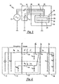
- FIGURE 1 shows a conventional capacitively-coupled, RF-plasma reactor system 10 for a PECVD system.
- the reactor system 10 includes an RF power supply 12, a matching network 14, a reactor chamber 16, and a vacuum chamber 18.
- the reactor chamber 16 includes two metallic plates 20, 22 arranged in parallel enclosed in a metallic-reactor casing 24.
- the first metallic plate 22 is electrically connected to the RF power supply 12 via a feeding element 26 and the matching network 14 and the first metallic plate 22 is, thus, a live electrode.
- the second metallic plate 20 is connected to ground and is, thus, a ground electrode. During the deposition process a substrate is placed on the second metallic plate 20 for processing.
- the feeding element 26 is shielded with a grounding shield 28 and can be any type of electrical feeding element known in the art, such as an RF stripline, RF ribbon, or a triplate stripline.
- a plasma-discharge region 30 is defined in between the two metallic plates 20, 22.
- the RF power supply 12 and matching network 14 are located outside the vacuum chamber 18 and the reactor chamber 16 and feeding element 26 are located inside the vacuum chamber 18.
- the RF power supply 12 and the matching network 14 are under atmospheric conditions and the reactor chamber 16 and RF feed line 28 are under vacuum conditions.
- a typical gas used for forming a plasma in the PECVD process is a silicon nitride SiN gas. Other gases commonly known in the art, however, may be used in this type of application such as organometallics, hydrides and halides.
- FIGURE 2 shows a simplified equivalent circuit of the conventional PECVD system during the deposition of SiN and will be used to illustrate the disadvantage of the conventional RF-plasma reactor system 10.
- the dotted line boxes represent a portion of the conventional RF-plasma reactor system 10 as indicated by the reference numbers.
- a disadvantage to this process in large area parallel plate reactors is that a very large parasitic-reactor capacitance C R , typically greater than 5000pF, forms between the live electrode 22 and the grounded reactor casing 24.
- the feeding element 26 must be capable of handling very large RF currents IF, typically greater than 300A.
- the large RF currents require a very wide stripline design, which leads to a second parasitic-feed-line capacitance C F between the live wire of the feeding element 26 and the grounding shield 28.
- the feed-line capacitance C F is typically greater than 3000pF.
- the reactor C R and feed-line C F capacitance transform a plasma impedance Z P to a feed-through impedance Re(Z F ) having a very small value, typically less than 0.05 ohms.
- the feed-through impedance Re(Z F ) is the impedance as seen at the entrance of the vacuum chamber 18 where the feeding element 26 enters the vacuum chamber 18.
- the feed-through impedance Re(Z F ) in turn creates a larger RF current IF, typically greater than 400A, which now must be accommodated by the matching network 14 and the feeding element 26.
- RF current IF typically greater than 400A
- most of the power delivered by the RF power supply is dissipated in the lossy elements R M , R F of the matching network 14 and the feeding element 26 respectively.
- the efficiency of the system is low, typically ⁇ s ⁇ 0.3. Therefore, very large and expensive RF power supplies are required in order to achieve the necessary plasma power density and deposition rate.
- the efficiency of the plasma power coupling efficiency decreases to values less than 20% at an RF frequency of 13.56MHz.
- the parasitic capacitance C R and C F could be reduced by increasing the gap between the live parts, i.e. the live electrode 22 and feeding element 26, and the grounded parts, i.e. the reactor casing 24 and the ground shield 28.
- the disadvantage to this solution is that the plasma between the gaps could ignite.
- Another solution is to water cool the reactor. This, however, is difficult in a vacuum system and water cooling does not significantly enhance the plasma coupling efficiency.
- Another solution is adding an impedance-transformation circuit to the RF-plasma reactor system 10. Power losses through the lossy elements R M , R F in the matching network 14 and the feeding element 26 respectively can be reduced by decreasing the RF current IF. Reducing the RF current IF while maintaining the plasma power can be accomplished with an impedance-transformation circuit, which increases the feed-through impedance Re(Z F ).
- an impedance-transformation circuit solely made of one inductor is impractical for several reasons. For example, the inductor needs to be a low-loss inductor, there is nothing to prevent the DC voltage from shorting to ground, and there is no tuning capability.
- a plasma reactor comprising, a vacuum chamber, a first metallic plate and a second metallic plate located inside the vacuum chamber, an RF power supply, a matching network, a plasma-discharge region containing plasma defined between the first and second metallic plates, a feeding element electrically connected to the first metallic plate, and an impedance-transformation circuit electrically connected to the first metallic plate.
- a plasma reactor comprising, a vacuum chamber, an RF power supply, a matching network, a first metallic plate and a second metallic plate located inside the vacuum chamber, a plasma-discharge region for containing plasma defined between the first and second metallic plates, a feeding element electrically connected to the first metallic plate, an impedance-transformation circuit electrically connected to the first metallic plate, comprising an isolation capacitor, later referred as blocking capacitor.
- a method of depositing semi-conductive layers in a vacuum comprising the steps of, providing a plasma reactor further including an RF power supply, a vacuum chamber, a reactor chamber, having a reactor impedance, located inside the vacuum chamber, a first and second metallic plate located inside the vacuum chamber; a plasma-discharge region for containing plasma defined between the first and second metallic plates, a feeding element electrically connected to the first metallic plate, and an impedance-transformation circuit electrically connected to the first metallic plate, placing a substrate on the second metallic plate, delivering RF power to the plasma, transforming the reactor impedance to an intermediate impedance with the impedance-transformation circuit, and transforming the intermediate impedance to a feed-through impedance with the feeding element, whereby the feed-through impedance is increased.
- the invention may take physical form in certain parts and arrangement of parts, a preferred embodiment of which will be described in detail in this specification and illustrated in the accompanying drawings that form a part of the specification.
- FIGURES 3 and 4 a more practical impedance-transformation circuit is shown in the schematic in FIGURE 3 and the electrical equivalent circuit in FIGURE 4 . All components described in FIGURES 1 and 2 above that are the same in FIGURES 3 and 4 will not be repeated.
- FIGURE 3 shows a capacitively-coupled, RF-plasma reactor system 40 (hereinafter “transformed RF-plasma reactor system”) for a PECVD system having an impendance-transformation circuit 42, shown in FIGURE 4 , in accordance with the present invention.
- the impedance-transformation circuit 42 includes a transformation circuit feeding element 44 with a grounding shield 46 and a tuneable-blocking capacitor C BT .
- the second feeding element 44 is represented in the equivalent circuit as having parasitic capacitance C T , a lossy element R T , and an low-loss inductor L T .
- the transformation circuit feeding element 44 is located inside the vacuum chamber 18 and is connected to ground via the tuneable-blocking capacitor C BT .
- the transformed RF-plasma reactor system 40 now includes the feeding element 26 and the transformation circuit feeding element 44 both of which are electrically connected to the first metallic plate 22.
- the tuneable-blocking capacitor C BT is located outside the vacuum chamber 18 and can be integrated into the matching network 14, resulting in amended matching network 14' ( Fig. 3 ).
- the tuneable-blocking capacitor C BT can increase the feed-through impedance Re(Z F ') thereby decreasing the total RF current IF' during the deposition process. Further, the tuneable-blocking capacitor C BT can balance the current between the two feeding elements 26, 44 without venting the system.
- the current I F ' flowing out of the matching network 14 and through the feeding element 26 is partially compensated by the current I T flowing through the transformation circuit element 44 and tuneable-blocking capacitor C BT .
- the optimal balance between IF'and I T can be adjusted through the timeable-blocking capacitor C BT and depends on the balance between the power losses of the lossy elements (R F '+R M ) of the feeding element 26 and matching network 14 and the lossy element R T of the transformation circuit feeding element 44.
- the power lost through the lossy elements R M , R F in the conventional RF-plasma reactor system 10 (no impedance-transformation circuit 42) are more than twice as much as the power lost through the lossy elements R M , R F ', R T in the transformed RF-plasma reactor system 40 with the impedance-transformation circuit 42.
- the power delivered to the plasma to maintain the same deposition rate as the conventional RF-plasma reactor system 10 (no impedance-transformation circuit 42) can be reduced.
- a smaller RF power supply can be used to achieve the same deposition rate.
- the same size RF power supply is used the deposition rate will increase thereby increasing throughput.
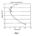
- FIGURE 5 shows a graph that illustrates how the impedance-transformation circuit 42 transforms the feed-through impedance Re(Z F ') to thereby decrease the power lost through the lossy elements.
- the plasma impedance Zp is transformed by a reactor capacitance C R and a reactor inductance L R to a reactor impedance Z R located at the end of the feeding element 26.
- the feeding element 26 then transforms the reactor impedance Z R to a feed-through impedance designated as Z F .
- the plasma impedance Z P is transformed to the reactor impedance Z R . just as in the conventional RF-plasma reactor system 10.
- the impedance-transformation circuit 42 transforms the reactor impedance Z R to an intermediate impedance Z R '.
- the feeding element 26 then transforms the intermediate impedance Z R ' to a feed-through impedance designated as Z F .
- the feed-through impedance Z F has both a higher resistive or real part and a higher inductive reactive or imaginary part than the feed-through impedance Z F .
- the real part of the feed-through impedance Re(Z F ) is approximately 0.1 to 0.2 ohms whereas the real part of the feed-through impedance Re(Z F ) is approximately 0.0 to 0.1 ohms.
- the imaginary part of the feed-through impedance Im(Z F ) is approximately 1 to 5 ohms whereas the imaginary part of the feed-through impedance Im(Z F ) is approximately -3 to 1 ohms.
- the impedance-transformation circuit 42 is not intended to compensate for reactive impedance or cancel out phase shifts.
- the more inductive the feed-through impedance Z F however, the less inductance is required in the matching network. As a result, the quality of the matching network can be enhanced even more because the RF power losses are mainly associated with lumped elements such as inductors made from copper.
Landscapes
- Physics & Mathematics (AREA)
- Engineering & Computer Science (AREA)
- Plasma & Fusion (AREA)
- Chemical & Material Sciences (AREA)
- Analytical Chemistry (AREA)
- Electromagnetism (AREA)
- Spectroscopy & Molecular Physics (AREA)
- Chemical Vapour Deposition (AREA)
- Plasma Technology (AREA)
- Multi-Conductor Connections (AREA)
Applications Claiming Priority (2)
| Application Number | Priority Date | Filing Date | Title |
|---|---|---|---|
| US62778404P | 2004-11-12 | 2004-11-12 | |
| PCT/CH2005/000669 WO2006050632A2 (en) | 2004-11-12 | 2005-11-11 | Impedance matching of a capacitively coupled rf plasma reactor suitable for large area substrates |
Publications (2)
| Publication Number | Publication Date |
|---|---|
| EP1812949A2 EP1812949A2 (en) | 2007-08-01 |
| EP1812949B1 true EP1812949B1 (en) | 2010-07-07 |
Family
ID=36218432
Family Applications (1)
| Application Number | Title | Priority Date | Filing Date |
|---|---|---|---|
| EP05801054A Not-in-force EP1812949B1 (en) | 2004-11-12 | 2005-11-11 | Impedance matching of a capacitively coupled rf plasma reactor suitable for large area substrates |
Country Status (10)
Families Citing this family (21)
| Publication number | Priority date | Publication date | Assignee | Title |
|---|---|---|---|---|
| KR100915613B1 (ko) * | 2007-06-26 | 2009-09-07 | 삼성전자주식회사 | 펄스 플라즈마 매칭시스템 및 그 방법 |
| KR100979186B1 (ko) | 2007-10-22 | 2010-08-31 | 다이나믹솔라디자인 주식회사 | 용량 결합 플라즈마 반응기 |
| TWI440405B (zh) * | 2007-10-22 | 2014-06-01 | New Power Plasma Co Ltd | 電容式耦合電漿反應器 |
| US20100018648A1 (en) * | 2008-07-23 | 2010-01-28 | Applied Marterials, Inc. | Workpiece support for a plasma reactor with controlled apportionment of rf power to a process kit ring |
| US8734664B2 (en) | 2008-07-23 | 2014-05-27 | Applied Materials, Inc. | Method of differential counter electrode tuning in an RF plasma reactor |
| US8578879B2 (en) * | 2009-07-29 | 2013-11-12 | Applied Materials, Inc. | Apparatus for VHF impedance match tuning |
| SG10201405040PA (en) * | 2009-08-31 | 2014-10-30 | Lam Res Corp | A local plasma confinement and pressure control arrangement and methods thereof |
| CN102487572B (zh) * | 2010-12-02 | 2015-06-24 | 理想能源设备(上海)有限公司 | 等离子加工装置 |
| TWI455172B (zh) * | 2010-12-30 | 2014-10-01 | Semes Co Ltd | 基板處理設備、電漿阻抗匹配裝置及可變電容器 |
| SI23611A (sl) | 2011-01-20 | 2012-07-31 | Institut@@quot@JoĹľef@Stefan@quot | Metoda in naprava za vzbujanje visokofrekvenčne plinske plazme |
| CN102686004B (zh) * | 2011-03-17 | 2015-05-13 | 中微半导体设备(上海)有限公司 | 用于等离子体发生器的可控制谐波的射频系统 |
| US8932429B2 (en) * | 2012-02-23 | 2015-01-13 | Lam Research Corporation | Electronic knob for tuning radial etch non-uniformity at VHF frequencies |
| CN102695353B (zh) * | 2012-05-31 | 2015-08-12 | 浙江工商大学 | 利用高电压产生气体等离子放电基本单元及反应器 |
| KR20150048812A (ko) | 2012-08-27 | 2015-05-07 | 에어로바이론먼트, 인크. | 휴대용 전기차 전원 공급장치 |
| CN103794895B (zh) * | 2012-10-30 | 2016-02-24 | 新奥光伏能源有限公司 | 一种射频电源接入器 |
| CN103388134B (zh) * | 2013-07-22 | 2016-05-18 | 北京工业大学 | 容性耦合等离子体增强化学气相沉积制备厚度均匀薄膜的方法 |
| CN103454489B (zh) * | 2013-09-12 | 2016-09-21 | 清华大学 | 匹配网络的损耗功率标定方法及系统 |
| US20180175819A1 (en) * | 2016-12-16 | 2018-06-21 | Lam Research Corporation | Systems and methods for providing shunt cancellation of parasitic components in a plasma reactor |
| US10536130B2 (en) * | 2017-08-29 | 2020-01-14 | Mks Instruments, Inc. | Balancing RF circuit and control for a cross-coupled SIMO distribution network |
| CN113169025A (zh) | 2018-12-21 | 2021-07-23 | 瑞士艾发科技 | 用于真空等离子体处理至少一个衬底或用于制造衬底的真空处理设备和方法 |
| US11107661B2 (en) * | 2019-07-09 | 2021-08-31 | COMET Technologies USA, Inc. | Hybrid matching network topology |
Family Cites Families (13)
| Publication number | Priority date | Publication date | Assignee | Title |
|---|---|---|---|---|
| US3143594A (en) * | 1960-07-13 | 1964-08-04 | Samuel E Derby | Demountable multiple stage ultra-high vacuum system |
| US3471396A (en) * | 1967-04-10 | 1969-10-07 | Ibm | R.f. cathodic sputtering apparatus having an electrically conductive housing |
| DE2939167A1 (de) * | 1979-08-21 | 1981-04-02 | Coulter Systems Corp., Bedford, Mass. | Vorrichtung und verfahren zur leistungszufuehrung an eine von dem entladungsplasma einer zerstaeubungsvorrichtung gebildeten last |
| JPH0354825A (ja) * | 1989-07-21 | 1991-03-08 | Tokyo Electron Ltd | プラズマ処理装置 |
| JPH0685542A (ja) * | 1992-09-03 | 1994-03-25 | Hitachi Metals Ltd | 周波数可変マイクロ波発振器 |
| US5981899A (en) * | 1997-01-17 | 1999-11-09 | Balzers Aktiengesellschaft | Capacitively coupled RF-plasma reactor |
| JP2961103B1 (ja) * | 1998-04-28 | 1999-10-12 | 三菱重工業株式会社 | プラズマ化学蒸着装置 |
| US6395095B1 (en) * | 1999-06-15 | 2002-05-28 | Tokyo Electron Limited | Process apparatus and method for improved plasma processing of a substrate |
| JP2002316040A (ja) * | 2001-04-24 | 2002-10-29 | Matsushita Electric Ind Co Ltd | プラズマ処理方法及び装置 |
| US6706138B2 (en) * | 2001-08-16 | 2004-03-16 | Applied Materials Inc. | Adjustable dual frequency voltage dividing plasma reactor |
| JP4216054B2 (ja) * | 2001-11-27 | 2009-01-28 | アルプス電気株式会社 | プラズマ処理装置及びその運転方法 |
| TW200300650A (en) * | 2001-11-27 | 2003-06-01 | Alps Electric Co Ltd | Plasma processing apparatus |
| JP4370789B2 (ja) * | 2002-07-12 | 2009-11-25 | 東京エレクトロン株式会社 | プラズマ処理装置及び可変インピーダンス手段の校正方法 |
-
2005
- 2005-11-11 DE DE602005022221T patent/DE602005022221D1/de active Active
- 2005-11-11 EP EP05801054A patent/EP1812949B1/en not_active Not-in-force
- 2005-11-11 CN CN2005800386843A patent/CN101057310B/zh not_active Expired - Fee Related
- 2005-11-11 AT AT05801054T patent/ATE473513T1/de not_active IP Right Cessation
- 2005-11-11 JP JP2007540474A patent/JP5086092B2/ja not_active Expired - Fee Related
- 2005-11-11 WO PCT/CH2005/000669 patent/WO2006050632A2/en active Application Filing
- 2005-11-11 KR KR1020077007856A patent/KR101107393B1/ko not_active Expired - Fee Related
- 2005-11-11 US US11/719,115 patent/US20070252529A1/en not_active Abandoned
- 2005-11-11 AU AU2005304253A patent/AU2005304253B8/en not_active Ceased
- 2005-11-14 TW TW094139874A patent/TW200625396A/zh unknown
Also Published As
| Publication number | Publication date |
|---|---|
| CN101057310B (zh) | 2010-11-03 |
| US20070252529A1 (en) | 2007-11-01 |
| KR101107393B1 (ko) | 2012-01-19 |
| WO2006050632A2 (en) | 2006-05-18 |
| EP1812949A2 (en) | 2007-08-01 |
| ATE473513T1 (de) | 2010-07-15 |
| JP5086092B2 (ja) | 2012-11-28 |
| AU2005304253B8 (en) | 2011-01-20 |
| AU2005304253A1 (en) | 2006-05-18 |
| DE602005022221D1 (de) | 2010-08-19 |
| KR20070099526A (ko) | 2007-10-09 |
| TW200625396A (en) | 2006-07-16 |
| AU2005304253B2 (en) | 2010-12-23 |
| CN101057310A (zh) | 2007-10-17 |
| WO2006050632A3 (en) | 2006-07-27 |
| JP2008520091A (ja) | 2008-06-12 |
Similar Documents
| Publication | Publication Date | Title |
|---|---|---|
| EP1812949B1 (en) | Impedance matching of a capacitively coupled rf plasma reactor suitable for large area substrates | |
| US4284490A (en) | R.F. Sputtering apparatus including multi-network power supply | |
| EP1269511B1 (en) | Plasma reactor with overhead rf electrode tuned to the plasma | |
| US6703080B2 (en) | Method and apparatus for VHF plasma processing with load mismatch reliability and stability | |
| US7102292B2 (en) | Method and device for removing harmonics in semiconductor plasma processing systems | |
| EP1225794B1 (en) | Matching device and plasma processing apparatus | |
| US7480571B2 (en) | Apparatus and methods for improving the stability of RF power delivery to a plasma load | |
| USRE39064E1 (en) | Electronic device manufacturing apparatus and method for manufacturing electronic device | |
| US8628640B2 (en) | Plasma processing unit and high-frequency electric power supplying unit | |
| US20130112666A1 (en) | Plasma processing apparatus | |
| EP0810816A1 (en) | Balanced source for plasma system | |
| JP2006502556A (ja) | 半導体ワークピースを処理するためのプラズマリアクタ | |
| WO2008118342A1 (en) | Rf shielded, series inductor, high rf power impedance matching interconnector for co2 slab laser | |
| US20050106873A1 (en) | Plasma chamber having multiple RF source frequencies | |
| US6838832B1 (en) | Apparatus and methods for improving the stability of RF power delivery to a plasma load | |
| JP4727377B2 (ja) | 真空処理装置、真空処理装置における高周波電力供給方法 | |
| KR100807908B1 (ko) | 부하 부정합 신뢰성 및 안정성을 갖는 vhf 플라즈마처리 방법 및 장치 |
Legal Events
| Date | Code | Title | Description |
|---|---|---|---|
| PUAI | Public reference made under article 153(3) epc to a published international application that has entered the european phase |
Free format text: ORIGINAL CODE: 0009012 |
|
| 17P | Request for examination filed |
Effective date: 20070612 |
|
| AK | Designated contracting states |
Kind code of ref document: A2 Designated state(s): AT BE BG CH CY CZ DE DK EE ES FI FR GB GR HU IE IS IT LI LT LU LV MC NL PL PT RO SE SI SK TR |
|
| 17Q | First examination report despatched |
Effective date: 20070907 |
|
| DAX | Request for extension of the european patent (deleted) | ||
| RAP1 | Party data changed (applicant data changed or rights of an application transferred) |
Owner name: OERLIKON TRADING AG, TRUEBBACH |
|
| GRAP | Despatch of communication of intention to grant a patent |
Free format text: ORIGINAL CODE: EPIDOSNIGR1 |
|
| GRAS | Grant fee paid |
Free format text: ORIGINAL CODE: EPIDOSNIGR3 |
|
| GRAA | (expected) grant |
Free format text: ORIGINAL CODE: 0009210 |
|
| AK | Designated contracting states |
Kind code of ref document: B1 Designated state(s): AT BE BG CH CY CZ DE DK EE ES FI FR GB GR HU IE IS IT LI LT LU LV MC NL PL PT RO SE SI SK TR |
|
| REG | Reference to a national code |
Ref country code: GB Ref legal event code: FG4D |
|
| REG | Reference to a national code |
Ref country code: CH Ref legal event code: EP |
|
| REG | Reference to a national code |
Ref country code: IE Ref legal event code: FG4D |
|
| REF | Corresponds to: |
Ref document number: 602005022221 Country of ref document: DE Date of ref document: 20100819 Kind code of ref document: P |
|
| REG | Reference to a national code |
Ref country code: NL Ref legal event code: VDEP Effective date: 20100707 |
|
| PG25 | Lapsed in a contracting state [announced via postgrant information from national office to epo] |
Ref country code: SI Free format text: LAPSE BECAUSE OF FAILURE TO SUBMIT A TRANSLATION OF THE DESCRIPTION OR TO PAY THE FEE WITHIN THE PRESCRIBED TIME-LIMIT Effective date: 20100707 |
|
| LTIE | Lt: invalidation of european patent or patent extension |
Effective date: 20100707 |
|
| PG25 | Lapsed in a contracting state [announced via postgrant information from national office to epo] |
Ref country code: NL Free format text: LAPSE BECAUSE OF FAILURE TO SUBMIT A TRANSLATION OF THE DESCRIPTION OR TO PAY THE FEE WITHIN THE PRESCRIBED TIME-LIMIT Effective date: 20100707 Ref country code: LT Free format text: LAPSE BECAUSE OF FAILURE TO SUBMIT A TRANSLATION OF THE DESCRIPTION OR TO PAY THE FEE WITHIN THE PRESCRIBED TIME-LIMIT Effective date: 20100707 Ref country code: FI Free format text: LAPSE BECAUSE OF FAILURE TO SUBMIT A TRANSLATION OF THE DESCRIPTION OR TO PAY THE FEE WITHIN THE PRESCRIBED TIME-LIMIT Effective date: 20100707 Ref country code: AT Free format text: LAPSE BECAUSE OF FAILURE TO SUBMIT A TRANSLATION OF THE DESCRIPTION OR TO PAY THE FEE WITHIN THE PRESCRIBED TIME-LIMIT Effective date: 20100707 |
|
| PG25 | Lapsed in a contracting state [announced via postgrant information from national office to epo] |
Ref country code: CY Free format text: LAPSE BECAUSE OF FAILURE TO SUBMIT A TRANSLATION OF THE DESCRIPTION OR TO PAY THE FEE WITHIN THE PRESCRIBED TIME-LIMIT Effective date: 20100707 Ref country code: PL Free format text: LAPSE BECAUSE OF FAILURE TO SUBMIT A TRANSLATION OF THE DESCRIPTION OR TO PAY THE FEE WITHIN THE PRESCRIBED TIME-LIMIT Effective date: 20100707 Ref country code: IS Free format text: LAPSE BECAUSE OF FAILURE TO SUBMIT A TRANSLATION OF THE DESCRIPTION OR TO PAY THE FEE WITHIN THE PRESCRIBED TIME-LIMIT Effective date: 20101107 Ref country code: BG Free format text: LAPSE BECAUSE OF FAILURE TO SUBMIT A TRANSLATION OF THE DESCRIPTION OR TO PAY THE FEE WITHIN THE PRESCRIBED TIME-LIMIT Effective date: 20101007 Ref country code: PT Free format text: LAPSE BECAUSE OF FAILURE TO SUBMIT A TRANSLATION OF THE DESCRIPTION OR TO PAY THE FEE WITHIN THE PRESCRIBED TIME-LIMIT Effective date: 20101108 |
|
| PG25 | Lapsed in a contracting state [announced via postgrant information from national office to epo] |
Ref country code: BE Free format text: LAPSE BECAUSE OF FAILURE TO SUBMIT A TRANSLATION OF THE DESCRIPTION OR TO PAY THE FEE WITHIN THE PRESCRIBED TIME-LIMIT Effective date: 20100707 Ref country code: LV Free format text: LAPSE BECAUSE OF FAILURE TO SUBMIT A TRANSLATION OF THE DESCRIPTION OR TO PAY THE FEE WITHIN THE PRESCRIBED TIME-LIMIT Effective date: 20100707 Ref country code: SE Free format text: LAPSE BECAUSE OF FAILURE TO SUBMIT A TRANSLATION OF THE DESCRIPTION OR TO PAY THE FEE WITHIN THE PRESCRIBED TIME-LIMIT Effective date: 20100707 Ref country code: GR Free format text: LAPSE BECAUSE OF FAILURE TO SUBMIT A TRANSLATION OF THE DESCRIPTION OR TO PAY THE FEE WITHIN THE PRESCRIBED TIME-LIMIT Effective date: 20101008 |
|
| PG25 | Lapsed in a contracting state [announced via postgrant information from national office to epo] |
Ref country code: DK Free format text: LAPSE BECAUSE OF FAILURE TO SUBMIT A TRANSLATION OF THE DESCRIPTION OR TO PAY THE FEE WITHIN THE PRESCRIBED TIME-LIMIT Effective date: 20100707 |
|
| PLBE | No opposition filed within time limit |
Free format text: ORIGINAL CODE: 0009261 |
|
| STAA | Information on the status of an ep patent application or granted ep patent |
Free format text: STATUS: NO OPPOSITION FILED WITHIN TIME LIMIT |
|
| PG25 | Lapsed in a contracting state [announced via postgrant information from national office to epo] |
Ref country code: IT Free format text: LAPSE BECAUSE OF FAILURE TO SUBMIT A TRANSLATION OF THE DESCRIPTION OR TO PAY THE FEE WITHIN THE PRESCRIBED TIME-LIMIT Effective date: 20100707 Ref country code: RO Free format text: LAPSE BECAUSE OF FAILURE TO SUBMIT A TRANSLATION OF THE DESCRIPTION OR TO PAY THE FEE WITHIN THE PRESCRIBED TIME-LIMIT Effective date: 20100707 Ref country code: EE Free format text: LAPSE BECAUSE OF FAILURE TO SUBMIT A TRANSLATION OF THE DESCRIPTION OR TO PAY THE FEE WITHIN THE PRESCRIBED TIME-LIMIT Effective date: 20100707 Ref country code: SK Free format text: LAPSE BECAUSE OF FAILURE TO SUBMIT A TRANSLATION OF THE DESCRIPTION OR TO PAY THE FEE WITHIN THE PRESCRIBED TIME-LIMIT Effective date: 20100707 Ref country code: CZ Free format text: LAPSE BECAUSE OF FAILURE TO SUBMIT A TRANSLATION OF THE DESCRIPTION OR TO PAY THE FEE WITHIN THE PRESCRIBED TIME-LIMIT Effective date: 20100707 |
|
| 26N | No opposition filed |
Effective date: 20110408 |
|
| PG25 | Lapsed in a contracting state [announced via postgrant information from national office to epo] |
Ref country code: ES Free format text: LAPSE BECAUSE OF FAILURE TO SUBMIT A TRANSLATION OF THE DESCRIPTION OR TO PAY THE FEE WITHIN THE PRESCRIBED TIME-LIMIT Effective date: 20101018 Ref country code: MC Free format text: LAPSE BECAUSE OF NON-PAYMENT OF DUE FEES Effective date: 20101130 |
|
| REG | Reference to a national code |
Ref country code: CH Ref legal event code: PL |
|
| REG | Reference to a national code |
Ref country code: DE Ref legal event code: R097 Ref document number: 602005022221 Country of ref document: DE Effective date: 20110408 |
|
| GBPC | Gb: european patent ceased through non-payment of renewal fee |
Effective date: 20101111 |
|
| PG25 | Lapsed in a contracting state [announced via postgrant information from national office to epo] |
Ref country code: CH Free format text: LAPSE BECAUSE OF NON-PAYMENT OF DUE FEES Effective date: 20101130 Ref country code: LI Free format text: LAPSE BECAUSE OF NON-PAYMENT OF DUE FEES Effective date: 20101130 |
|
| REG | Reference to a national code |
Ref country code: FR Ref legal event code: ST Effective date: 20110801 |
|
| PG25 | Lapsed in a contracting state [announced via postgrant information from national office to epo] |
Ref country code: FR Free format text: LAPSE BECAUSE OF NON-PAYMENT OF DUE FEES Effective date: 20101130 Ref country code: IE Free format text: LAPSE BECAUSE OF NON-PAYMENT OF DUE FEES Effective date: 20101111 |
|
| PG25 | Lapsed in a contracting state [announced via postgrant information from national office to epo] |
Ref country code: GB Free format text: LAPSE BECAUSE OF NON-PAYMENT OF DUE FEES Effective date: 20101111 |
|
| REG | Reference to a national code |
Ref country code: DE Ref legal event code: R081 Ref document number: 602005022221 Country of ref document: DE Owner name: TEL SOLAR AG, CH Free format text: FORMER OWNER: OERLIKON TRADING AG, TRUEBBACH, TRUEBBACH, CH Effective date: 20120123 |
|
| PG25 | Lapsed in a contracting state [announced via postgrant information from national office to epo] |
Ref country code: HU Free format text: LAPSE BECAUSE OF FAILURE TO SUBMIT A TRANSLATION OF THE DESCRIPTION OR TO PAY THE FEE WITHIN THE PRESCRIBED TIME-LIMIT Effective date: 20110108 Ref country code: LU Free format text: LAPSE BECAUSE OF NON-PAYMENT OF DUE FEES Effective date: 20101111 |
|
| PG25 | Lapsed in a contracting state [announced via postgrant information from national office to epo] |
Ref country code: TR Free format text: LAPSE BECAUSE OF FAILURE TO SUBMIT A TRANSLATION OF THE DESCRIPTION OR TO PAY THE FEE WITHIN THE PRESCRIBED TIME-LIMIT Effective date: 20100707 |
|
| REG | Reference to a national code |
Ref country code: DE Ref legal event code: R082 Ref document number: 602005022221 Country of ref document: DE Representative=s name: MICHALSKI HUETTERMANN & PARTNER PATENTANWAELTE, DE |
|
| REG | Reference to a national code |
Ref country code: DE Ref legal event code: R082 Ref document number: 602005022221 Country of ref document: DE Representative=s name: MICHALSKI HUETTERMANN & PARTNER PATENTANWAELTE, DE Effective date: 20130731 Ref country code: DE Ref legal event code: R081 Ref document number: 602005022221 Country of ref document: DE Owner name: TEL SOLAR AG, CH Free format text: FORMER OWNER: OERLIKON SOLAR AG, TRUEBBACH, TRUEBBACH, CH Effective date: 20130731 |
|
| PGFP | Annual fee paid to national office [announced via postgrant information from national office to epo] |
Ref country code: DE Payment date: 20141105 Year of fee payment: 10 |
|
| REG | Reference to a national code |
Ref country code: DE Ref legal event code: R119 Ref document number: 602005022221 Country of ref document: DE |
|
| PG25 | Lapsed in a contracting state [announced via postgrant information from national office to epo] |
Ref country code: DE Free format text: LAPSE BECAUSE OF NON-PAYMENT OF DUE FEES Effective date: 20160601 |