EP1811566A2 - Three-dimensional Multi-Chips and tri-axial sensors and methods of manufacuring the same - Google Patents
Three-dimensional Multi-Chips and tri-axial sensors and methods of manufacuring the same Download PDFInfo
- Publication number
- EP1811566A2 EP1811566A2 EP07100559A EP07100559A EP1811566A2 EP 1811566 A2 EP1811566 A2 EP 1811566A2 EP 07100559 A EP07100559 A EP 07100559A EP 07100559 A EP07100559 A EP 07100559A EP 1811566 A2 EP1811566 A2 EP 1811566A2
- Authority
- EP
- European Patent Office
- Prior art keywords
- axis sensor
- sensor die
- recited
- leadframe
- die
- Prior art date
- Legal status (The legal status is an assumption and is not a legal conclusion. Google has not performed a legal analysis and makes no representation as to the accuracy of the status listed.)
- Granted
Links
Images


Classifications
-
- G—PHYSICS
- G01—MEASURING; TESTING
- G01P—MEASURING LINEAR OR ANGULAR SPEED, ACCELERATION, DECELERATION, OR SHOCK; INDICATING PRESENCE, ABSENCE, OR DIRECTION, OF MOVEMENT
- G01P15/00—Measuring acceleration; Measuring deceleration; Measuring shock, i.e. sudden change of acceleration
- G01P15/18—Measuring acceleration; Measuring deceleration; Measuring shock, i.e. sudden change of acceleration in two or more dimensions
-
- B—PERFORMING OPERATIONS; TRANSPORTING
- B81—MICROSTRUCTURAL TECHNOLOGY
- B81B—MICROSTRUCTURAL DEVICES OR SYSTEMS, e.g. MICROMECHANICAL DEVICES
- B81B7/00—Microstructural systems ; Auxiliary parts of microstructural devices or systems
- B81B7/0032—Packages or encapsulation
- B81B7/0074—3D packaging, i.e. encapsulation containing one or several MEMS devices arranged in planes non-parallel to the mounting board
-
- G—PHYSICS
- G01—MEASURING; TESTING
- G01D—MEASURING NOT SPECIALLY ADAPTED FOR A SPECIFIC VARIABLE; ARRANGEMENTS FOR MEASURING TWO OR MORE VARIABLES NOT COVERED IN A SINGLE OTHER SUBCLASS; TARIFF METERING APPARATUS; MEASURING OR TESTING NOT OTHERWISE PROVIDED FOR
- G01D11/00—Component parts of measuring arrangements not specially adapted for a specific variable
- G01D11/24—Housings ; Casings for instruments
- G01D11/245—Housings for sensors
-
- G—PHYSICS
- G01—MEASURING; TESTING
- G01P—MEASURING LINEAR OR ANGULAR SPEED, ACCELERATION, DECELERATION, OR SHOCK; INDICATING PRESENCE, ABSENCE, OR DIRECTION, OF MOVEMENT
- G01P1/00—Details of instruments
- G01P1/02—Housings
- G01P1/023—Housings for acceleration measuring devices
-
- H—ELECTRICITY
- H10—SEMICONDUCTOR DEVICES; ELECTRIC SOLID-STATE DEVICES NOT OTHERWISE PROVIDED FOR
- H10W—GENERIC PACKAGES, INTERCONNECTIONS, CONNECTORS OR OTHER CONSTRUCTIONAL DETAILS OF DEVICES COVERED BY CLASS H10
- H10W90/00—Package configurations
- H10W90/701—Package configurations characterised by the relative positions of pads or connectors relative to package parts
- H10W90/751—Package configurations characterised by the relative positions of pads or connectors relative to package parts of bond wires
- H10W90/753—Package configurations characterised by the relative positions of pads or connectors relative to package parts of bond wires between laterally-adjacent chips
-
- H—ELECTRICITY
- H10—SEMICONDUCTOR DEVICES; ELECTRIC SOLID-STATE DEVICES NOT OTHERWISE PROVIDED FOR
- H10W—GENERIC PACKAGES, INTERCONNECTIONS, CONNECTORS OR OTHER CONSTRUCTIONAL DETAILS OF DEVICES COVERED BY CLASS H10
- H10W90/00—Package configurations
- H10W90/701—Package configurations characterised by the relative positions of pads or connectors relative to package parts
- H10W90/751—Package configurations characterised by the relative positions of pads or connectors relative to package parts of bond wires
- H10W90/756—Package configurations characterised by the relative positions of pads or connectors relative to package parts of bond wires between a chip and a stacked lead frame, conducting package substrate or heat sink
Definitions
- dies The goal of the manufacture, or packaging, of integrated circuits and other electronic devices, collectively referred to herein as "dies", is to protect the die during fabrication and during use without affecting its ability to perform as it was designed to perform.
- dies are packaged using a variety of materials that can include plastics, ceramics, metals, and the like.
- plastic packaging With plastic packaging, a die is attached to a leadframe and both are covered with an insulative material or the like. With ceramic and metal packaging, the die is placed in a hermetically sealed environment. The exorbitant cost of metal and, to a lesser extent, ceramic packaging with respect to plastic packaging makes plastic packaging the method of choice for all but a few, unique applications.
- the die or plurality of dies is first attached to a substrate, e.g., a leadframe or another die or chip, and operationally connected to a number of interconnections, e.g., interconnection pads, interconnection bumps or the like.
- a substrate e.g., a leadframe or another die or chip
- interconnections e.g., interconnection pads, interconnection bumps or the like.
- Means of operationally connecting the die or plurality of dies to the substrate can include soldering, wire bonding, flip-chip bonding, tape-automated bonding, and the like.
- Flip-chip bonding also involves attaching a substrate having a plurality of interconnection leads, pads or the like and a die having a plurality of preformed bumps, solder balls or the like. Typically, when mounting the die, the die is inverted, or "flipped" so that the leads are between the die and the substrate. Once the preformed bumps or solder balls of the die are aligned with the interconnection leads of the substrate, the preformed solder bumps are re-heated, e.g., by solder reflow, above the melting point of the solder to effect the assembly, or surface mounting, of the die and the substrate. Ultrasonic and adhesive bonding can also be used.
- TAB Tape-automated bonding
- a TAB assembly comprising a metal foil on which a lead pattern is etched, between a substrate and a die.
- the lead pattern can be intricate and/or include a multiplicity of input/output interconnections.
- the TAB assembly can further include, e.g., adhesives, polymeric material, and interconnection bumps.
- 3D packaging has followed trends and developments of two-dimensional (“2D”) packaging. More specifically, the 3D approach has been to increase density by merely layering or stacking 2D packages and, in some applications, to stack elements or dies on edge.
- the elements associated with this latter application include each of the dies, the interconnections between dies, attachments between dies, and the leads.
- 3D packaging offers advantages in package density, system power, and electrical performance, the disadvantages include poor yields, thermal dissipation shortcomings, and cross-talk. Therefore, it is desirable to provide novel packaging for three-dimensional devices, e.g., sensors and the like, and to provide methods of manufacturing the same.
- devices for providing tri-axial measurements in an x-direction, a y-direction, and a z-direction and methods of their manufacture.
- the devices comprise a leadframe, one or more X- and Y-axis sensor dies, an integrated circuit, and a Z-axis sensor.
- the leadframe, X- and Y-axis sensor dies, integrated circuit, and the Z-axis sensor die are encapsulated in a plastic material to provide a final molding.
- the leadframe includes a preformed vertical or substantially vertical paddle to which the Z-axis sensor die is in physical and/or operational communication.
- the leadframe includes a sub-paddle and a plurality of leadframe legs and, further, the Z-axis sensor die is attached to the sub-paddle and the plurality of leadframe legs so that the sensing direction of the Z-axis sensor die is orthogonal or substantially orthogonal to the sensing directions of the X- and Y-axis sensor dies.
- the sensing direction of the Z-axis sensor die with respect to the leadframe legs is in or substantially in the same plane as the legs; however, the leadframe legs can be reconfigured, e.g., bent or rotated, so that the re-configured portions of the leadframe legs and the Z-axis sensor die are orthogonal or substantially orthogonal to the sensing directions of the X- and Y-axis sensor dies.
- the Z-axis sensor die, a portion of the leadframe, and a portion of the input/output pads are encapsulated to provide a pre-molding that is then encapsulated in the final molding.
- the X- and Y-axis sensor dies, a portion of the leadframe, the integrated circuit, and a portion of the input/output pads are encapsulated to provide a pre-molding that is then encapsulated in the final molding.
- Methods of manufacturing these devices comprise providing a leadframe, a plurality of input/output leads, and a plurality of Z-axis sensor leads; attaching one or more X- and Y-axis sensor dies and one or more integrated circuits to the leadframe and the leads; attaching a Z-axis sensor die to the leadframe and the Z-axis sensor leads so that the sensing direction is orthogonal or substantially orthogonal to sensing directions of the X- and Y-axis sensor dies; and encapsulating the leadframe, the input/output leads, the Z-axis sensor leads, the X- and Y-axis sensor dies, the integrated circuits, and the Z-axis sensor die in a final molding.
- the step of attaching the Z-axis sensor includes, further, attaching the Z-axis sensor die to the input/output leads and to the Z-axis sensor leads so that its sensing direction is in the same or substantially the same plane as the sensing directions of the X- and Y-axis sensor dies.
- the Z-axis sensor die, a portion of the input/output leads, and a portion of the Z-axis sensor lead are pre-encapsulated and the pre-encapsulated Z-axis sensor die can be re-configured so that the sensing direction is orthogonal or substantially orthogonal to the sensing directions of the X- and Y-axis sensor dies.
- the devices for providing tri-axial measurements comprise a base substrate having an inner cavity, one or more X- and Y-axis sensor dies, and Z daughter board bonding with a Z-axis sensor die.
- a slotted portion is provided in each side wall of a pair of opposing side walls in the inner cavity for mounting the Z-axis sensor die vertically.
- the slotted portion includes a plurality of input/output pads and a plurality of interconnection pads that are structured and arranged in the bottom portion of the inner cavity.
- the methods of manufacturing the devices comprise providing a base substrate having a cavity portion; attaching one or more X- and Y-axis sensor dies to the base; and attaching a Z-axis sensor die to the base substrate so that the sensing direction is orthogonal or substantially orthogonal to sensing directions of the X- and Y-axis sensor dies.
- the step of attaching the Z-axis sensor die includes bonding the Z-axis sensor to the daughter board; providing a slotted portion in opposing side walls of the cavity; and installing the Z-axis daughter board, with the sensor die attached, into the slotted portion so that the sensing direction of the Z-axis sensor die is orthogonal or substantially orthogonal to the sensing directions of the X- and Y-axis sensor dies.
- the devices for providing tri-axial measurements comprise a base substrate having an inner cavity, one or more X- and Y-axis sensor dies, and a Z-axis sensor die.
- a plurality of input/output pads and a plurality of interconnection pads that are structured and arranged in the side wall of the sub-cavity are provided.
- the methods of manufacturing the devices comprise providing a base substrate having a cavity portion; attaching one or more X- and Y-axis sensor dies to the base substrate; and attaching a Z-axis sensor die to a side wall, e.g., by soldering, so that the sensing direction is orthogonal or substantially orthogonal to sensing directions of the X- and Y-axis sensor dies.
- the devices for providing tri-axial measurements comprise a flexible carrier, one or more X- and Y-axis sensor dies, one or more integrated circuits, a Z-axis sensor die, and a more rigid, L-type substrate.
- the Z-axis sensor die is disposed on a distal end portion of the flexible carrier and the distal end portion is bent or rotated about 90 degrees with respect to the horizontal, so that the distal end portion is oriented orthogonal or substantially orthogonal to the flexible carrier.
- the device further comprises a final molding that encapsulates the flexible carrier, the X- and Y-axis sensor dies, the one or more integrated circuits, the z-axis sensor, and the rigid substrate.
- the method of manufacturing this device comprises structuring and arranging a Z-axis sensor die, X- and Y-axis sensor dies, and integrated circuits to a flexible carrier; reconfiguring that portion of the flexible carrier having the Z-axis sensor die so that it is vertical or substantially vertical with respect to the flexible carrier and, further, so that the sensing direction of the Z-axis sensor die is orthogonal or substantially orthogonal to sensing directions of the X- and Y-axis sensor dies; structuring and arranging the flexible carrier to a more rigid, L-type substrate; and encapsulating the substrate, the flexible carrier, the X- and Y-axis sensor dies, the integrated circuits, and the Z-axis sensor die in a molding.
- the devices for providing tri-axial measurements comprise a base substrate, one or more X- and Y-axis sensor dies; one or more integrated circuits; a cube carrier; and one or more Z-axis sensor dies.
- the method of its manufacture comprises attaching the a cube carrier to the base substrate; attaching the X- and Y-axis sensor dies to the base substrate; attaching the integrated circuits to the base substrate; attaching the Z-axis sensor dies to one or more of the vertical faces of the cube carrier; and encapsulating the base substrate, the cube carrier, the X- and Y-axis dies, the integrated circuits, and the Z-axis sensor dies in a molding.
- 3D multi-chips Disclosed are three-dimensional (3D) multi-chips and methods of their manufacture, or "packaging". In describing the various embodiments of the devices, methods of their manufacture will be described concurrently. Furthermore, although the 3D multi-chips will be described in terms of a 3D multi-chip for use as a tri-axial sensor, the invention is not to be construed as being limited thereto.
- a first embodiment of the present invention in two stages of manufacture. Shown is a substrate, a carrier or a leadframe 10 having a preformed vertical portion, or paddle 12.
- the vertical paddle 12 shown is orthogonal or substantially orthogonal to the leadframe 10, the invention is not to be construed as being limited to a perfectly vertical paddle 12 that forms a right angle with the leadframe 10. Indeed, the invention can also be practiced with the paddle 12 forming an acute angle, and obtuse angle, and/or an angle that deviates slightly from perfectly vertical with the leadframe 10.
- a plurality of input/output (I/O) interconnections, or pads 16 is structured and arranged in the same or substantially the same plane and along the axis of the leadframe 10 in a manner well known to those of ordinary skill in the art.
- preformed leads to the Z-axis sensor die 14 and 18 are structured and arranged in proximity of and on either side of the vertical paddle 12.
- some portion of the preformed leads 14 and 18 also is in or substantially in the same plane as the leadframe 10 and the I/O pads 16.
- the invention is not to be construed as being limited to just four preformed leads 14 and 18. Indeed, the invention can also be practiced with fewer or more leadframe legs.
- the Z-axis sensor die 13 is fixedly and operatively attached, e.g., by soldering, by adhesives, by wire-bonding, by flip-chip bonding, and the like, to the vertical paddle 12 of the leadframe 10.
- Bonding wires, or leads, 11 provide operational communication between the Z-axis sensor die 13 and the preformed leads 14 and 18.
- the leads 11, the vertical paddle 12, the Z-axis sensor die 13, and some portion of the preformed leads 14 and 18 are encapsulated in a pre-molding 15 in any manner that is known to those of ordinary skill in the art.
- the encapsulating material for the pre-molding can include as examples and without limitation, plastics, polymers, polyamides, epoxies, and the like.
- ASIC application-specific integrated circuit
- Leads or wires 11 provide operational communication between the X- and Y-axis sensor die(s) 17 and the ASIC 19, between the X- and Y-axis sensor die(s) 17 and the I/O pads 16, between the ASIC 19 and the preformed leads 14 and 18, and between the ASIC 19 and the I/O pads 16.
- the leadframe 10, the ASIC 19, the I/O pads 16, the X- and Y-axis sensor die(s) 17, and the pre-molding 15 can be encapsulated in a final molding 1 in any manner that is known to those of ordinary skill in the art.
- the encapsulating material for the pre-molding can include as examples and without limitation, plastics, polymers, polyamides, epoxies, and the like.
- the final molding 1 can then be trimmed and formed as necessary. Electroplating and other processes can also be performed on the exposed portions of the I/O pads 16 and the preformed leads 14 and 18.
- a second embodiment of the present invention in two stages of manufacture. Shown is a substrate, carrier or leadframe 20 comprising a plurality of leadframe legs 22 that interconnect a main leadframe island 28a to a leadframe sub-island 28b. Although two leadframe legs 22 are shown interconnecting the main leadframe island 28a to the leadframe sub-island 28b, the invention is not to be construed as being limited to just two leadframe legs 22. Indeed, the invention can also be practiced with one or more leadframe legs 22.
- a plurality of I/O interconnections or pads 26 is structured and arranged in the same or substantially the same plane and along the x- or y-axis of the main leadframe island 28a in a manner well known to those of ordinary skill in the art.
- the Z-axis sensor die leads 24 are structured and arranged in the same or substantially the same plane of the leadframe legs 22.
- the invention is not to be construed as being limited to just two Z-axis sensor die leads 24. Indeed, the invention can also be practiced with fewer or more Z-axis sensor die leads 24.
- the Z-axis sensor die 23 is fixedly and operationally attached, e.g., by soldering, by adhesives, by wire-bonding, by flip-chip bonding, and the like, to the leadframe sub-portion 28b of the leadframe 20.
- Figs. 2A and 2B show the Z-axis sensor 23 disposed on the top, or upper side, of the leadframe sub-island 28b, the Z-axis sensor 23, alternatively, could be disposed on the bottom, or under side, of the leadframe sub-island 28b.
- the Z-axis sensor die 23 is attached to the leadframe sub-island 28b so that the initial sensing direction Z is in the same direction as the x- or y-axis of the leadframe legs 22 and the Z-axis sensor die leads 24 as shown by the arrow in FIG. 2A.
- Bonding wires, or leads, 21 provide operational communication between the Z-axis sensor die 23, the Z-axis sensor die leads 24, and each of the leadframe legs 22.
- the leads 21, the Z-axis sensor die 23, some portion of the Z-axis sensor die leads 24, and some portion of the leadframe legs 22 are encapsulated in a pre-molding 25 in any manner that is known to those of ordinary skill in the art.
- the encapsulating material for the pre-molding can include as examples and without limitation, plastics, polymers, polyamides, epoxies, and the like.
- the sensing direction Z of the Z-axis sensor die 23 can be made orthogonal or substantially orthogonal to the plane of the leadframe 20, preferably, by re-configuring the pre-molding 25. More specifically, the sensing direction Z of the Z-axis sensor die 23 can be made orthogonal or substantially orthogonal to the plane of the leadframe 20 by rotating or bending the pre-molding 25 approximately 90 degrees from the horizontal so that the pre-molding 25 itself is orthogonal or substantially orthogonal to the plane of the leadframe 20.
- one or more X- and Y-axis sensor dies 27 and an ASIC 29 can be fixedly and operationally attached, e.g., by soldering, by adhesives, by wire-bonding, by flip-chip bonding, and the like, to the leadframe 20.
- Leads 21 provide operational communication between the X- and Y-axis sensor die(s) 27 and the ASIC 29, between the X- and Y-axis sensor die(s) 27 and the I/O pads 26, between the ASIC 29 and the encapsulated Z-axis sensor die 23, and between the X- and Y-axis sensor die(s) 27 and the encapsulated Z-axis sensor die 23.
- the leadframe 20, the ASIC 29, the I/O pads 26, the X- and Y-axis sensor die(s) 27, and the pre-molding 25 can be encapsulated in a final molding 2 in any manner that is known to those of ordinary skill in the art.
- the encapsulating material for the pre-molding can include as examples and without limitation, plastics, polymers, polyamides, epoxies, and the like.
- the final molding 2 can then be trimmed and formed as necessary. Electroplating and other processes can also be performed on the exposed portions of the I/O pads 26, some portion of the Z-axis sensor die leads 24, and some portion of the leadframe legs 22.
- a third embodiment of the present invention in two stages of manufacture. Shown is a substrate, a carrier or a leadframe 30 comprising a main leadframe island 38 and a plurality of leadframe legs 32 connected thereto. Although only two leadframe legs 32 are shown connected to the main leadframe island 38, that the invention is not to be construed as being limited to just two leadframe legs 32. Indeed, the invention can also be practiced with one or more leadframe legs 32.
- a plurality of I/O interconnections or pads 36 is structured and arranged in the same or substantially the same plane and about the x- or y-axis of the main leadframe island 38 in a manner well known to those of ordinary skill in the art.
- the Z-axis sensor leads 34 are also structured and arranged in the same or substantially the same plane of the leadframe legs 32.
- the invention is not to be construed as being limited to just two Z-axis sensor die leads 34. Indeed, the invention can also be practiced with fewer or more Z-axis sensor die leads 34.
- the Z-axis sensor 33 can be a pre-packaged independent component or a pre-packaged silicon chip.
- the pre-packaged Z-axis sensor 33 comprises a plurality of I/O pads 35, e.g., external pins, leadless leads, bumping pads, and the like.
- the plurality of I/O pads 35 is structured and arranged on one or more sides of the Z-axis sensor 33.
- the location of I/O pads 35 on the Z-axis sensor 33 should align with the leadframe legs 32 and the Z-axis sensor leads 34, e.g., four to four as shown in Fig. 3A.
- the Z-axis sensor 33 is fixedly and operationally attached, e.g., by soldering, by adhesives, by flip-chip bonding, by solder reflow, and the like, to the leadframe legs 32 and to the Z-axis sensor preformed leads 34. Because the Z-axis sensor 33 comes with its own I/O pads 35, bonding wires are not necessary to connect the Z-axis sensor 33 to the other components.
- solder joints 41 are shown in Figs. 3A and 3B. If the I/O pads 35 are structured and arranged on two sides of the Z-axis sensor 33 as shown in Fig. 3A, the solder joint 41 covers the exposed portion of the I/O pad 35.
- each of the leadframe legs 32 and each of the Z-axis sensor leads 34 are arranged to be in registration with a discrete I/O pad 35.
- the Z-axis sensor 33 is fixedly and operationally attached to the leadframe legs 32 and to the Z-axis sensor leads 34 so that the sensing direction Z is orthogonal or substantially orthogonal to the plane of the leadframe 30.
- one or more X- and Y-axis sensor dies 37 and an ASIC 39 can be fixedly and operationally attached, e.g., by soldering, by adhesives, by wire-bonding, by flip-chip bonding, and the like, to the leadframe 30.
- Leads 31 provide operational communication between the X- and Y-axis sensor die(s) 37 and the ASIC 39, between the X- and Y-axis sensor die(s) 37 and the I/O pads 36, between the ASIC 39 and the Z-axis sensor 33, and between the X- and Y-axis sensor die(s) 37 and the Z-axis sensor 33.
- the leads 31, the ASIC 39, the leadframe 30, the I/O pads 36, the X- and Y-axis sensor die(s) 37, and the Z-axis sensor 33 can be encapsulated in a final molding 3 in any manner that is known to those of ordinary skill in the art.
- the encapsulating material for the final molding can include as examples and without limitation, plastics, polymers, polyamides, epoxies, and the like.
- the final molding 3 can then be trimmed and formed as necessary. Electroplating and other processes can also be performed on the exposed portions of the I/O pads 36, the leadframe legs 32, and the Z-axis sensor leads 34.
- the manufacturing sequence can be modified slightly as depicted in Figs. 4A and 4B.
- the one or more X- and Y-axis sensor dies 47 and an ASIC 49 can be fixedly and operationally attached, e.g., by soldering, by adhesives, by wire-bonding, by flip-chip bonding, and the like, to the leadframe 40.
- leads 31 provide operational communication between the X- and Y-axis sensor die(s) 47 and the ASIC 49, between the X- and Y-axis sensor die(s) 47 and the I/O pads 46, between the ASIC 49, a first lead leg 42a, and a first Z-axis sensor lead 44a, and between the X- and Y-axis sensor die(s) 47, a second lead leg 42b, and a second Z-axis sensor lead 44b.
- the lead legs 42a and 42b and Z-axis sensor leads 44a and 44b have been arrayed to be in registration with a plurality of I/O pads 45 on the Z-axis sensor 43, the ASIC 49, the leadframe 40, the I/O pads 46, the X- and Y-axis sensor die(s) 47, and portions of the lead legs 42a and 42b and the Z-axis sensor leads 44a and 44b can be encapsulated in a pre-molding 48 in any manner that is known to those of ordinary skill in the art.
- the encapsulating material for the pre-molding can include as examples and without limitation, plastics, polymers, polyamides, epoxies, and the like.
- the Z-axis sensor 43 can be a pre-packaged independent component or a pre-packaged silicon chip.
- the Z-axis sensor 43 comprises a plurality of I/O pads 45, e.g., external pins, leadless leads, bumping pads, and the like. More preferably, the plurality of I/O pads 45 is structured and arranged on one or more sides of the Z-axis sensor 43. The location of I/O pads 45 on the Z-axis sensor 43 should align with leadframe legs 42a and 42b and Z-axis sensor leads 44a and 44b, e.g., four to four as shown in Fig. 4A.
- the Z-axis sensor 43 is fixedly attached, e.g., by soldering, by adhesives, by flip-chip bonding, and the like, to the leadframe legs 42a and 42b and the Z-axis sensor leads 44a and 44b.
- solder joints 41 are shown in Fig. 4B. If the plurality of I/O pads 45 are structured and arranged on two sides of the Z-axis sensor 43 as shown in Fig. 4A, the solder joint 41 covers the exposed portion of the I/O pad 45.
- the Z-axis sensor 43 is fixedly and operationally attached to the leadframe legs 42a and 42b and to the Z-axis sensor leads 44a and 44b so that the sensing direction Z is orthogonal or substantially orthogonal to the plane of the leadframe 40. Because the pre-packaged Z-axis sensor 43 comes with its own I/O pads 45, bonding wires are not necessary to connect the Z-axis sensor 43 to the leadframe legs 42a and 42b or to the Z-axis sensor leads 44a and 44b.
- the pre-molding 48, the exposed portions of the leadframe legs 42a and 42b, the Z-axis sensor leads 44a and 44b, and the Z-axis sensor 43 can be encapsulated in a final molding 4 in any manner that is known to those of ordinary skill in the art.
- the encapsulating material for the final molding can include as examples and without limitation, plastics, polymers, polyamides, epoxies, and the like.
- the final molding 4 can then be trimmed and formed as necessary. Electroplating and other processes can also be performed on the exposed portions of the I/O pads 46.
- a fifth embodiment of the present invention in two stages of manufacture. Shown is a preformed base substrate, or package, 58, e.g., a ceramic package, pre-molding plastic cavity package or a package of some other rigid material, e.g., metal, alloy, and the like.
- the base substrate 58 has been hollowed out and/or pre-molded to include a cavity 91.
- the base substrate 58 has been preformed or machined to include a plurality of external I/O interconnections or pads 95, which have been disposed on two or more of the exterior side walls 94a and 94b.
- the cavity 91 includes a pair of opposing side walls 92a and 92b, each side wall 92a and 92b having a shelf portion 93 that houses a plurality of internal interconnection pads 55a, and that, further, includes a slotted portion 54.
- the slotted portions 54 on each of the pair of opposing side walls 92a and 92b are in registration with each other.
- a plurality of internal interconnection pads 55b is provided at the cavity bottom 96 between the opposing slotted portions 54.
- one or more X- and Y-axis sensor dies 57 is fixedly and operationally attached, e.g., by soldering, by adhesives, by wire-bonding, by flip-chip bonding, and the like, to the cavity bottom 96 between the shelf portions 93 and the plurality of interconnection pads 55a. Bonding wires, or leads, 51a provide operational communication between the X- and Y-axis sensor die(s) 57 and the interconnection pads 55a.
- the integrated circuit (not shown) can be integrally designed with the X- and Y-axis sensor dies 57 or stacked above or below the X- and Y-axis sensor dies 57 or disposed on the same plane as the X- and Y-axis sensor dies 57.
- a Z-axis sensor die 53 is fixedly and operationally attached, e.g., by soldering, by adhesives, by wire-bonding, by flip-chip bonding, and the like, to a Z-axis substrate carrier 52 to provide a Z-axis sensor unit 50 having a sensing capability in sensing direction Z.
- the Z-axis substrate carrier 52 includes a plurality of bonding pads 51b, e.g., external pins, leadless leads, bumping pads, and the like, that is structured and arranged on the face to which the Z-axis sensor die 53 is fixedly attached.
- a plurality of I/O bonding pads 56a is structured and arranged on the face of the Z-axis sensor die 53 that is opposite the sensing direction Z, i.e., in the negative Z - direction.
- a plurality of leads 51a provides operational communication between the Z-axis sensor die 53 and the plurality of bonding pads 51b.
- the Z-axis sensor unit 50 can be attached, e.g., by soldering, by adhesives, by solder reflow, and the like, to the base substrate 58 via the slotted portions 54.
- Each I/O pads 56a on the Z-axis sensor unit 50 is structured and arranged to be in registration with a discrete interconnection pads 55b disposed on the base substrate 58 between the slotted portions 54.
- the Z-axis sensor unit 50 is attached to the base substrate 58 so that the initial sensing direction Z is orthogonal or substantially orthogonal to the plane of the bottom portion 96 of the package 58. Because the Z-axis sensor unit 50 comes with its own I/O pads 56a, bonding wires are not necessary to connect the Z-axis sensor unit 50 to the interconnection pads 55b.
- the Z-axis sensor unit 50 is operationally positioned in a sub-cavity area 59 of the package 58 so that the Z-axis substrate carrier 52 is disposed between the Z-axis sensor unit 50 and the X- and Y-axis sensor die(s) 57.
- the sub-cavity area 59 provides space for moving parts associated with the Z-axis sensor unit 50.
- the Z-axis sensor unit 50 can be attached to the base substrate 58 prior to attaching the X- and Y-axis sensor die(s) 57 without violating the scope and spirit of this disclosure.
- a sixth embodiment of the present invention in two stages of manufacture. Shown is a preformed base substrate, or package, 68, e.g., a ceramic package or a package of some other rigid material. During manufacture, the base substrate 68 is hollowed out and/or is preformed to include a cavity 91. Moreover, a plurality of external I/O interconnections or pads 95 has been disposed on two or more of the exterior side walls 94a and 94b.
- the cavity 91 includes a pair of opposing side walls 92a and 92b, each side wall 92a and 92b having a shelf portion 93, which houses a plurality of internal I/O interconnections or pads 55a, and a side wall shelf 97.
- the side wall shelf 97 is discontinuous and, moreover, the discontinuous side wall shelf 97 includes a plurality of interconnection pads 65b that are structured and arranged on either side of a Z-sensor substrate cavity 69.
- the sub-cavity area 69 provides space for moving parts associated with the Z-axis sensor.
- one or more X- and Y-axis sensor dies 67 is fixedly and operationally attached, e.g., by soldering, by adhesives, by wire-bonding, by flip-chip bonding, and the like, to the cavity bottom 96 between the shelf portions 93 and the plurality of interconnection pads 65a.
- Leads 61a provide operational communication between the X- and Y-axis sensor die(s) 67 and the interconnection pads 65a.
- the integrated circuit (not shown) can be integrally designed with the X- and Y-axis sensor dies 67 or stacked above or below the X- and Y-axis sensor dies 67 or disposed on the same plane as the X- and Y-axis sensor dies 67.
- a bumping Z-axis sensor die or a pre-packaged Z-axis sensor unit 63 includes a plurality of bonding pads 61, e.g., external pins, leadless leads, bumping pads, and the like, that is structured and arranged on the long face of the Z-axis sensor unit 63.
- the bonding pads 61 on the Z-axis sensor 63 are structured and arranged to be in registration with each of the interconnection pads 65b disposed on the base substrate 68.
- the Z-axis sensor unit 63 is operationally positioned along the Z-axis sensor die side wall 62 and fixedly attached, e.g., by soldering, by adhesives, by flip-chip bonding, and the like, to the interconnection pads 65b. Because the Z-axis sensor unit 63 has its own bonding pads 61, bonding wires are not necessary to connect the Z-axis sensor unit 63 to the interconnection pads 65b. Furthermore, the Z-axis sensor unit 63 is attached to the base substrate 68 so that the sensing direction Z is orthogonal or substantially orthogonal to the plane of the bottom portion 96 of the package 68.
- the seventh embodiment comprises a flexible carrier 72 to which the Z-axis sensor die 73, one or more X- and Y-axis sensor dies 77, and the ASIC 79 are fixedly and operationally attached.
- the flexible carrier 72 is made of a pliable material, e.g., a printed circuit board (PCB), so that it can be re-configured to provide a vertical of substantially vertical portion 74 at one end.
- the flexible carrier 72 can be fixedly attached to a base substrate 70 that also includes a preformed, vertical of substantially vertical portion 71 at one end, e.g., an L-type substrate.
- the Z-axis sensor die 73, the X- and Y-axis sensor die(s) 77, and the ASIC 79 are bonded, e.g., wire-bonded, flip-chip bonded, and the like, or otherwise fixedly attached to the flexible carrier 72.
- each of the Z-axis sensor die 73, the X- and Y-axis sensor die(s) 77, and the ASIC 79 is bonded to the flexible carrier 72 while the upper surface of the flexible carrier 72 is planar or substantially planar.
- the Z-axis sensor die 73 is bonded near a distal end of the flexible carrier 72 and the sensing direction Z of the Z-axis sensor die 72 lies in the plane of the flexible carrier 72.
- the portion of the flexible carrier 72 nearest the distal end to which the Z-axis sensor die 73 is bonded is re-configured, e.g., bent and rotated about 90 degrees from the horizontal, to provide a vertical of substantially vertical portion 74.
- the bent portion 74 of the flexible carrier 72 is bent and rotated so that the sensing direction Z of the Z-axis sensor die 72 is now orthogonal or substantially orthogonal to the plane of the flexible carrier 72.
- the invention is not to be construed as being limited to just one side bonding. Indeed, the invention can also be practiced with double side bonding for the flexible carrier 72.
- the flexible carrier 72 can then be fixedly attached, e.g., by wire bonding, by bump bonding, by adhesive, by soldering, and the like, to the L-type substrate 70.
- the vertical portion 74 of the flexible carrier 72 can be adhesively attached to the vertical support of L-type substrate 70.
- I/O pads (not shown) on the flexible carrier 72 can be connected to pads (not shown) in horizontal plane of the L-type substrate 70.
- the flexible carrier 72 is attached so that the vertical of substantially vertical portion 74 of the flexible carrier 72 and the Z-axis sensor die 73 attached thereto are supported by the vertical of substantially vertical portion 71 of the L-type substrate 70.
- the I/O connections and leads can be structured and arranged on the bottom of the L-type substrate 70.
- the L-type substrate 70 is a leadframe, the I/O connections and leads (not shown) can be structured and arranged by trimming and forming.
- the entire device can be encapsulated in a resin molding 75.
- the eighth embodiment comprises a multi-layered carrier 82 (herein after a "cube carrier''), made of, e.g., ceramic or PCB materials, that is fixedly and operationally attached to a base substrate 80.
- the cube carrier 82 provides a rigid, multi-layer structure, e.g., PCB, ceramic, pre-molded leadframe, and the like, having a plurality of I/O interconnections or pads 86 on up to six (6) faces of the cube 82.
- At least one Z-axis sensor die 83a and 83b can be fixedly attached, e.g., by soldering, by wire-bonding, by adhesive, by flip-chip bonding, and the like, to the cube carrier 82.
- the cube carrier 82 in turn, can be fixedly attached to the base substrate 80, e.g., through know surface-mounting technology (SMT) reflow soldering, flip-chip bonding, and the like.
- SMT know surface-mounting technology
- the one or more X- and Y-axis sensor dies 87 and ASIC 89 can be fixedly and operationally attached, e.g., by soldering, by wire-bonding, by adhesive, by flip-chip bonding, and the like, to each other and to the base substrate 80.
- the leads 81 from I/O pads 84 that are structured and arranged on the X- and Y-axis sensor die(s) 87 can be fixedly and operationally attached, e.g., by soldering, by wire-bonding, by flip-chip bonding, by adhesive, and the like, to corresponding I/O pads 85 that are structured and arranged on the substrate 80.
- the one or more X- and Y-axis sensor dies 87 and ASIC 89 are operationally interconnected, e.g., by soldering, by wire-bonding, by flip-chip bonding, by adhesive, and the like, through a plurality of interconnections (not shown) that are structured and arranged on each of the X- and Y-axis sensor die(s) 87 and ASIC 89 and the ASIC 89 and the base substrate 80 are operationally connected, e.g., by soldering, by wire-bonding, by flip-chip bonding, by adhesive, and the like, through a plurality of interconnections (not shown) that are structured and arranged on each of the ASIC 89 and the base substrate 80.
- the device above the base substrate 80 can be encapsulated to provide a molding 8.
- underfilling beneath the Z-axis sensor die, the X- and Y-axis sensor die(s), and ASIC to encapsulate the bonding areas may be required.
- wire-bonding pre-encapsulation of the Z-axis sensor die, the X- and Y-axis sensor die(s) may also be required.
Landscapes
- Physics & Mathematics (AREA)
- General Physics & Mathematics (AREA)
- Engineering & Computer Science (AREA)
- Microelectronics & Electronic Packaging (AREA)
- Computer Hardware Design (AREA)
- Lead Frames For Integrated Circuits (AREA)
- Structures Or Materials For Encapsulating Or Coating Semiconductor Devices Or Solid State Devices (AREA)
- Gyroscopes (AREA)
Abstract

Description
- The goal of the manufacture, or packaging, of integrated circuits and other electronic devices, collectively referred to herein as "dies", is to protect the die during fabrication and during use without affecting its ability to perform as it was designed to perform. Typically, dies are packaged using a variety of materials that can include plastics, ceramics, metals, and the like.
- With plastic packaging, a die is attached to a leadframe and both are covered with an insulative material or the like. With ceramic and metal packaging, the die is placed in a hermetically sealed environment. The exorbitant cost of metal and, to a lesser extent, ceramic packaging with respect to plastic packaging makes plastic packaging the method of choice for all but a few, unique applications.
- Typically, during manufacture, the die or plurality of dies is first attached to a substrate, e.g., a leadframe or another die or chip, and operationally connected to a number of interconnections, e.g., interconnection pads, interconnection bumps or the like. Means of operationally connecting the die or plurality of dies to the substrate can include soldering, wire bonding, flip-chip bonding, tape-automated bonding, and the like.
- Traditional soldering and wire-bonding provide a metallurgical bond between a bonding wire, or lead, on the die and an interconnection pad that has been pre-printed or preformed on the surface of the substrate.
- Flip-chip bonding also involves attaching a substrate having a plurality of interconnection leads, pads or the like and a die having a plurality of preformed bumps, solder balls or the like. Typically, when mounting the die, the die is inverted, or "flipped" so that the leads are between the die and the substrate. Once the preformed bumps or solder balls of the die are aligned with the interconnection leads of the substrate, the preformed solder bumps are re-heated, e.g., by solder reflow, above the melting point of the solder to effect the assembly, or surface mounting, of the die and the substrate. Ultrasonic and adhesive bonding can also be used.
- Tape-automated bonding (TAB) involves interposing a TAB assembly, comprising a metal foil on which a lead pattern is etched, between a substrate and a die. Typically, the lead pattern can be intricate and/or include a multiplicity of input/output interconnections. The TAB assembly can further include, e.g., adhesives, polymeric material, and interconnection bumps. Once the TAB assembly has been interposed and the die and substrate have been properly aligned, the TAB assembly is bonded to the die and the substrate, e.g., by ultrasonic bonding.
- To date, three-dimensional ("3D") packaging has followed trends and developments of two-dimensional ("2D") packaging. More specifically, the 3D approach has been to increase density by merely layering or stacking 2D packages and, in some applications, to stack elements or dies on edge. The elements associated with this latter application include each of the dies, the interconnections between dies, attachments between dies, and the leads.
- Although 3D packaging offers advantages in package density, system power, and electrical performance, the disadvantages include poor yields, thermal dissipation shortcomings, and cross-talk. Therefore, it is desirable to provide novel packaging for three-dimensional devices, e.g., sensors and the like, and to provide methods of manufacturing the same.
- In accordance with the present invention, devices are disclosed for providing tri-axial measurements in an x-direction, a y-direction, and a z-direction and methods of their manufacture. The devices comprise a leadframe, one or more X- and Y-axis sensor dies, an integrated circuit, and a Z-axis sensor. In one embodiment, the leadframe, X- and Y-axis sensor dies, integrated circuit, and the Z-axis sensor die are encapsulated in a plastic material to provide a final molding.
- In still another aspect of this embodiment, the leadframe includes a preformed vertical or substantially vertical paddle to which the Z-axis sensor die is in physical and/or operational communication.
- In one aspect of this embodiment, the leadframe includes a sub-paddle and a plurality of leadframe legs and, further, the Z-axis sensor die is attached to the sub-paddle and the plurality of leadframe legs so that the sensing direction of the Z-axis sensor die is orthogonal or substantially orthogonal to the sensing directions of the X- and Y-axis sensor dies.
- In still another aspect of this embodiment, initially, the sensing direction of the Z-axis sensor die with respect to the leadframe legs is in or substantially in the same plane as the legs; however, the leadframe legs can be reconfigured, e.g., bent or rotated, so that the re-configured portions of the leadframe legs and the Z-axis sensor die are orthogonal or substantially orthogonal to the sensing directions of the X- and Y-axis sensor dies.
- In yet another aspect of this embodiment, the Z-axis sensor die, a portion of the leadframe, and a portion of the input/output pads are encapsulated to provide a pre-molding that is then encapsulated in the final molding. Alternatively, the X- and Y-axis sensor dies, a portion of the leadframe, the integrated circuit, and a portion of the input/output pads are encapsulated to provide a pre-molding that is then encapsulated in the final molding.
- Methods of manufacturing these devices comprise providing a leadframe, a plurality of input/output leads, and a plurality of Z-axis sensor leads; attaching one or more X- and Y-axis sensor dies and one or more integrated circuits to the leadframe and the leads; attaching a Z-axis sensor die to the leadframe and the Z-axis sensor leads so that the sensing direction is orthogonal or substantially orthogonal to sensing directions of the X- and Y-axis sensor dies; and encapsulating the leadframe, the input/output leads, the Z-axis sensor leads, the X- and Y-axis sensor dies, the integrated circuits, and the Z-axis sensor die in a final molding.
- In one aspect of the embodied method, the step of attaching the Z-axis sensor includes, further, attaching the Z-axis sensor die to the input/output leads and to the Z-axis sensor leads so that its sensing direction is in the same or substantially the same plane as the sensing directions of the X- and Y-axis sensor dies. For example, the Z-axis sensor die, a portion of the input/output leads, and a portion of the Z-axis sensor lead are pre-encapsulated and the pre-encapsulated Z-axis sensor die can be re-configured so that the sensing direction is orthogonal or substantially orthogonal to the sensing directions of the X- and Y-axis sensor dies.
- In another embodiment, the devices for providing tri-axial measurements comprise a base substrate having an inner cavity, one or more X- and Y-axis sensor dies, and Z daughter board bonding with a Z-axis sensor die. In one aspect of this embodiment, a slotted portion is provided in each side wall of a pair of opposing side walls in the inner cavity for mounting the Z-axis sensor die vertically. In another aspect of this embodiment, the slotted portion includes a plurality of input/output pads and a plurality of interconnection pads that are structured and arranged in the bottom portion of the inner cavity.
- The methods of manufacturing the devices comprise providing a base substrate having a cavity portion; attaching one or more X- and Y-axis sensor dies to the base; and attaching a Z-axis sensor die to the base substrate so that the sensing direction is orthogonal or substantially orthogonal to sensing directions of the X- and Y-axis sensor dies. In one aspect of the embodied method, the step of attaching the Z-axis sensor die includes bonding the Z-axis sensor to the daughter board; providing a slotted portion in opposing side walls of the cavity; and installing the Z-axis daughter board, with the sensor die attached, into the slotted portion so that the sensing direction of the Z-axis sensor die is orthogonal or substantially orthogonal to the sensing directions of the X- and Y-axis sensor dies.
- In another embodiment, the devices for providing tri-axial measurements comprise a base substrate having an inner cavity, one or more X- and Y-axis sensor dies, and a Z-axis sensor die. In one aspect of this embodiment, a plurality of input/output pads and a plurality of interconnection pads that are structured and arranged in the side wall of the sub-cavity are provided.
- The methods of manufacturing the devices comprise providing a base substrate having a cavity portion; attaching one or more X- and Y-axis sensor dies to the base substrate; and attaching a Z-axis sensor die to a side wall, e.g., by soldering, so that the sensing direction is orthogonal or substantially orthogonal to sensing directions of the X- and Y-axis sensor dies.
- In yet another embodiment, the devices for providing tri-axial measurements comprise a flexible carrier, one or more X- and Y-axis sensor dies, one or more integrated circuits, a Z-axis sensor die, and a more rigid, L-type substrate. In one aspect of this embodiment, the Z-axis sensor die is disposed on a distal end portion of the flexible carrier and the distal end portion is bent or rotated about 90 degrees with respect to the horizontal, so that the distal end portion is oriented orthogonal or substantially orthogonal to the flexible carrier. In another aspect of this embodiment, the device further comprises a final molding that encapsulates the flexible carrier, the X- and Y-axis sensor dies, the one or more integrated circuits, the z-axis sensor, and the rigid substrate.
- The method of manufacturing this device comprises structuring and arranging a Z-axis sensor die, X- and Y-axis sensor dies, and integrated circuits to a flexible carrier; reconfiguring that portion of the flexible carrier having the Z-axis sensor die so that it is vertical or substantially vertical with respect to the flexible carrier and, further, so that the sensing direction of the Z-axis sensor die is orthogonal or substantially orthogonal to sensing directions of the X- and Y-axis sensor dies; structuring and arranging the flexible carrier to a more rigid, L-type substrate; and encapsulating the substrate, the flexible carrier, the X- and Y-axis sensor dies, the integrated circuits, and the Z-axis sensor die in a molding.
- In yet another embodiment, the devices for providing tri-axial measurements comprise a base substrate, one or more X- and Y-axis sensor dies; one or more integrated circuits; a cube carrier; and one or more Z-axis sensor dies. The method of its manufacture comprises attaching the a cube carrier to the base substrate; attaching the X- and Y-axis sensor dies to the base substrate; attaching the integrated circuits to the base substrate; attaching the Z-axis sensor dies to one or more of the vertical faces of the cube carrier; and encapsulating the base substrate, the cube carrier, the X- and Y-axis dies, the integrated circuits, and the Z-axis sensor dies in a molding.
- The invention will be more fully understood by referring to the Detailed Description of the Invention in conjunction with the Drawings, of which:
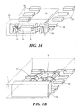
- Figs. 1A and 1B provide an illustrative example of a three-dimensional multi-chip and/or tri-axial sensor in two stages of manufacture in accordance with a first embodiment of the present invention;
- Figs. 2A and 2B provide an illustrative example of a three-dimensional multi-chip and/or tri-axial sensor in two stages of manufacture in accordance with a second embodiment of the present invention;
- Figs. 3A and 3B provide an illustrative example of a three-dimensional multi-chip and/or tri-axial sensor in two stages of manufacture in accordance with a third embodiment of the present invention;
- Figs. 4A and 4B provide an illustrative example of a three-dimensional multi-chip and/or tri-axial sensor in two stages of manufacture in accordance with a fourth embodiment of the present invention;
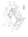
- Figs. 5A and 5B provide an illustrative example of a three-dimensional multi-chip and/or tri-axial sensor in two stages of manufacture in accordance with a fifth embodiment of the present invention;
- Figs. 6A and 6B provide an illustrative example of a three-dimensional multi-chip and/or tri-axial sensor in two stages of manufacture in accordance with a sixth embodiment of the present invention;
- Fig. 7 provides an illustrative example of a three-dimensional multi-chip and/or tri-axial sensor in two stages of manufacture in accordance with a seventh embodiment of the present invention; and
- Fig. 8 provides an illustrative example of a three-dimensional multi-chip and/or tri-axial sensor in two stages of manufacture in accordance with an eighth embodiment of the present invention.
- Disclosed are three-dimensional (3D) multi-chips and methods of their manufacture, or "packaging". In describing the various embodiments of the devices, methods of their manufacture will be described concurrently. Furthermore, although the 3D multi-chips will be described in terms of a 3D multi-chip for use as a tri-axial sensor, the invention is not to be construed as being limited thereto.
- Referring to Figs. 1A and 1B there is shown a first embodiment of the present invention in two stages of manufacture. Shown is a substrate, a carrier or a
leadframe 10 having a preformed vertical portion, orpaddle 12. Although thevertical paddle 12 shown is orthogonal or substantially orthogonal to theleadframe 10, the invention is not to be construed as being limited to a perfectlyvertical paddle 12 that forms a right angle with theleadframe 10. Indeed, the invention can also be practiced with thepaddle 12 forming an acute angle, and obtuse angle, and/or an angle that deviates slightly from perfectly vertical with theleadframe 10. - A plurality of input/output (I/O) interconnections, or
pads 16 is structured and arranged in the same or substantially the same plane and along the axis of theleadframe 10 in a manner well known to those of ordinary skill in the art. In one aspect of the present embodiment, preformed leads to the Z-axis sensor die 14 and 18 are structured and arranged in proximity of and on either side of thevertical paddle 12. In another aspect of the present embodiment, some portion of the preformed leads 14 and 18 also is in or substantially in the same plane as theleadframe 10 and the I/O pads 16. The invention is not to be construed as being limited to just four preformed leads 14 and 18. Indeed, the invention can also be practiced with fewer or more leadframe legs. - In one aspect of the first embodiment, the Z-axis sensor die 13 is fixedly and operatively attached, e.g., by soldering, by adhesives, by wire-bonding, by flip-chip bonding, and the like, to the
vertical paddle 12 of theleadframe 10. Bonding wires, or leads, 11 provide operational communication between the Z-axis sensor die 13 and the preformed leads 14 and 18. The leads 11, thevertical paddle 12, the Z-axis sensor die 13, and some portion of the preformed leads 14 and 18 are encapsulated in a pre-molding 15 in any manner that is known to those of ordinary skill in the art. The encapsulating material for the pre-molding can include as examples and without limitation, plastics, polymers, polyamides, epoxies, and the like. - Once the
vertical paddle 12 and the Z-axis sensor die 13 are encapsulated in the pre-molding 15, one or more X- and Y-axis sensor dies 17 and anintegrated circuit 19, e.g., typically, an application-specific integrated circuit (ASIC), can be fixedly and operationally attached, e.g., by soldering, by adhesives, by flip-chip bonding, by wire-bonding, and the like, to theleadframe 10. Leads orwires 11 provide operational communication between the X- and Y-axis sensor die(s) 17 and theASIC 19, between the X- and Y-axis sensor die(s) 17 and the I/O pads 16, between theASIC 19 and the preformed leads 14 and 18, and between theASIC 19 and the I/O pads 16. Once all of theleads 11 have been properly connected, theleadframe 10, theASIC 19, the I/O pads 16, the X- and Y-axis sensor die(s) 17, and the pre-molding 15 can be encapsulated in afinal molding 1 in any manner that is known to those of ordinary skill in the art. The encapsulating material for the pre-molding can include as examples and without limitation, plastics, polymers, polyamides, epoxies, and the like. - The
final molding 1 can then be trimmed and formed as necessary. Electroplating and other processes can also be performed on the exposed portions of the I/O pads 16 and the preformed leads 14 and 18. - Referring to Figs. 2A and 2B, there is shown a second embodiment of the present invention in two stages of manufacture. Shown is a substrate, carrier or
leadframe 20 comprising a plurality ofleadframe legs 22 that interconnect amain leadframe island 28a to aleadframe sub-island 28b. Although twoleadframe legs 22 are shown interconnecting themain leadframe island 28a to theleadframe sub-island 28b, the invention is not to be construed as being limited to just twoleadframe legs 22. Indeed, the invention can also be practiced with one ormore leadframe legs 22. - A plurality of I/O interconnections or
pads 26 is structured and arranged in the same or substantially the same plane and along the x- or y-axis of themain leadframe island 28a in a manner well known to those of ordinary skill in the art. The Z-axis sensor die leads 24 are structured and arranged in the same or substantially the same plane of theleadframe legs 22. The invention is not to be construed as being limited to just two Z-axis sensor die leads 24. Indeed, the invention can also be practiced with fewer or more Z-axis sensor die leads 24. - In one aspect of the second embodiment, the Z-axis sensor die 23 is fixedly and operationally attached, e.g., by soldering, by adhesives, by wire-bonding, by flip-chip bonding, and the like, to the
leadframe sub-portion 28b of theleadframe 20. Although Figs. 2A and 2B show the Z-axis sensor 23 disposed on the top, or upper side, of theleadframe sub-island 28b, the Z-axis sensor 23, alternatively, could be disposed on the bottom, or under side, of theleadframe sub-island 28b. In one aspect of this embodiment, the Z-axis sensor die 23 is attached to theleadframe sub-island 28b so that the initial sensing direction Z is in the same direction as the x- or y-axis of theleadframe legs 22 and the Z-axis sensor die leads 24 as shown by the arrow in FIG. 2A. Bonding wires, or leads, 21 provide operational communication between the Z-axis sensor die 23, the Z-axis sensor die leads 24, and each of theleadframe legs 22. - In another aspect of the second embodiment, the
leads 21, the Z-axis sensor die 23, some portion of the Z-axis sensor die leads 24, and some portion of theleadframe legs 22 are encapsulated in a pre-molding 25 in any manner that is known to those of ordinary skill in the art. The encapsulating material for the pre-molding can include as examples and without limitation, plastics, polymers, polyamides, epoxies, and the like. - Once the Z-axis sensor die 23 is encapsulated, the sensing direction Z of the Z-axis sensor die 23 can be made orthogonal or substantially orthogonal to the plane of the
leadframe 20, preferably, by re-configuring the pre-molding 25. More specifically, the sensing direction Z of the Z-axis sensor die 23 can be made orthogonal or substantially orthogonal to the plane of theleadframe 20 by rotating or bending the pre-molding 25 approximately 90 degrees from the horizontal so that the pre-molding 25 itself is orthogonal or substantially orthogonal to the plane of theleadframe 20. - After the pre-molding 25 has been re-configured, one or more X- and Y-axis sensor dies 27 and an
ASIC 29 can be fixedly and operationally attached, e.g., by soldering, by adhesives, by wire-bonding, by flip-chip bonding, and the like, to theleadframe 20. Leads 21 provide operational communication between the X- and Y-axis sensor die(s) 27 and theASIC 29, between the X- and Y-axis sensor die(s) 27 and the I/O pads 26, between theASIC 29 and the encapsulated Z-axis sensor die 23, and between the X- and Y-axis sensor die(s) 27 and the encapsulated Z-axis sensor die 23. Once all of theleads 21 have been connected, theleadframe 20, theASIC 29, the I/O pads 26, the X- and Y-axis sensor die(s) 27, and the pre-molding 25 can be encapsulated in afinal molding 2 in any manner that is known to those of ordinary skill in the art. - The encapsulating material for the pre-molding can include as examples and without limitation, plastics, polymers, polyamides, epoxies, and the like. The
final molding 2 can then be trimmed and formed as necessary. Electroplating and other processes can also be performed on the exposed portions of the I/O pads 26, some portion of the Z-axis sensor die leads 24, and some portion of theleadframe legs 22. - Referring to Figs. 3A and 3B, there is shown a third embodiment of the present invention in two stages of manufacture. Shown is a substrate, a carrier or a
leadframe 30 comprising amain leadframe island 38 and a plurality ofleadframe legs 32 connected thereto. Although only twoleadframe legs 32 are shown connected to themain leadframe island 38, that the invention is not to be construed as being limited to just twoleadframe legs 32. Indeed, the invention can also be practiced with one ormore leadframe legs 32. - A plurality of I/O interconnections or
pads 36 is structured and arranged in the same or substantially the same plane and about the x- or y-axis of themain leadframe island 38 in a manner well known to those of ordinary skill in the art. The Z-axis sensor leads 34 are also structured and arranged in the same or substantially the same plane of theleadframe legs 32. The invention is not to be construed as being limited to just two Z-axis sensor die leads 34. Indeed, the invention can also be practiced with fewer or more Z-axis sensor die leads 34. - In one aspect of the third embodiment, the Z-
axis sensor 33 can be a pre-packaged independent component or a pre-packaged silicon chip. The pre-packaged Z-axis sensor 33 comprises a plurality of I/O pads 35, e.g., external pins, leadless leads, bumping pads, and the like. The plurality of I/O pads 35 is structured and arranged on one or more sides of the Z-axis sensor 33. The location of I/O pads 35 on the Z-axis sensor 33 should align with theleadframe legs 32 and the Z-axis sensor leads 34, e.g., four to four as shown in Fig. 3A. - In another aspect of the present embodiment, the Z-
axis sensor 33 is fixedly and operationally attached, e.g., by soldering, by adhesives, by flip-chip bonding, by solder reflow, and the like, to theleadframe legs 32 and to the Z-axis sensor preformed leads 34. Because the Z-axis sensor 33 comes with its own I/O pads 35, bonding wires are not necessary to connect the Z-axis sensor 33 to the other components. - For illustrative purposes only, solder joints 41 are shown in Figs. 3A and 3B. If the I/
O pads 35 are structured and arranged on two sides of the Z-axis sensor 33 as shown in Fig. 3A, the solder joint 41 covers the exposed portion of the I/O pad 35. - In another aspect of the third embodiment, prior to attaching the Z-
axis sensor 33, each of theleadframe legs 32 and each of the Z-axis sensor leads 34 are arranged to be in registration with a discrete I/O pad 35. As shown in Fig. 3A, the Z-axis sensor 33 is fixedly and operationally attached to theleadframe legs 32 and to the Z-axis sensor leads 34 so that the sensing direction Z is orthogonal or substantially orthogonal to the plane of theleadframe 30. - After the pre-packaged Z-
axis sensor 33 has been attached to theleadframe legs 32 and to the Z-axis sensor leads 34, one or more X- and Y-axis sensor dies 37 and anASIC 39 can be fixedly and operationally attached, e.g., by soldering, by adhesives, by wire-bonding, by flip-chip bonding, and the like, to theleadframe 30. Leads 31 provide operational communication between the X- and Y-axis sensor die(s) 37 and theASIC 39, between the X- and Y-axis sensor die(s) 37 and the I/O pads 36, between theASIC 39 and the Z-axis sensor 33, and between the X- and Y-axis sensor die(s) 37 and the Z-axis sensor 33. - Once all of the
leads 31 have been connected, theleads 31, theASIC 39, theleadframe 30, the I/O pads 36, the X- and Y-axis sensor die(s) 37, and the Z-axis sensor 33 can be encapsulated in afinal molding 3 in any manner that is known to those of ordinary skill in the art. The encapsulating material for the final molding can include as examples and without limitation, plastics, polymers, polyamides, epoxies, and the like. Thefinal molding 3 can then be trimmed and formed as necessary. Electroplating and other processes can also be performed on the exposed portions of the I/O pads 36, theleadframe legs 32, and the Z-axis sensor leads 34. - Alternatively, in a fourth embodiment, the manufacturing sequence can be modified slightly as depicted in Figs. 4A and 4B. More particularly, the one or more X- and Y-axis sensor dies 47 and an
ASIC 49 can be fixedly and operationally attached, e.g., by soldering, by adhesives, by wire-bonding, by flip-chip bonding, and the like, to theleadframe 40. Furthermore, leads 31 provide operational communication between the X- and Y-axis sensor die(s) 47 and theASIC 49, between the X- and Y-axis sensor die(s) 47 and the I/O pads 46, between theASIC 49, a firstlead leg 42a, and a first Z-axis sensor lead 44a, and between the X- and Y-axis sensor die(s) 47, a secondlead leg 42b, and a second Z-axis sensor lead 44b. - Once all of the
leads 31 have been connected and thelead legs O pads 45 on the Z-axis sensor 43, theASIC 49, theleadframe 40, the I/O pads 46, the X- and Y-axis sensor die(s) 47, and portions of thelead legs - As with the third embodiment, the Z-
axis sensor 43 can be a pre-packaged independent component or a pre-packaged silicon chip. The Z-axis sensor 43 comprises a plurality of I/O pads 45, e.g., external pins, leadless leads, bumping pads, and the like. More preferably, the plurality of I/O pads 45 is structured and arranged on one or more sides of the Z-axis sensor 43. The location of I/O pads 45 on the Z-axis sensor 43 should align withleadframe legs - The Z-
axis sensor 43 is fixedly attached, e.g., by soldering, by adhesives, by flip-chip bonding, and the like, to theleadframe legs O pads 45 are structured and arranged on two sides of the Z-axis sensor 43 as shown in Fig. 4A, the solder joint 41 covers the exposed portion of the I/O pad 45. - In one aspect of the fourth embodiment, the Z-
axis sensor 43 is fixedly and operationally attached to theleadframe legs leadframe 40. Because the pre-packaged Z-axis sensor 43 comes with its own I/O pads 45, bonding wires are not necessary to connect the Z-axis sensor 43 to theleadframe legs - Once the Z-
axis sensor 43 is fixedly attached, the pre-molding 48, the exposed portions of theleadframe legs axis sensor 43 can be encapsulated in afinal molding 4 in any manner that is known to those of ordinary skill in the art. The encapsulating material for the final molding can include as examples and without limitation, plastics, polymers, polyamides, epoxies, and the like. Thefinal molding 4 can then be trimmed and formed as necessary. Electroplating and other processes can also be performed on the exposed portions of the I/O pads 46. - Whereas embodiments one through four disclose a flat or substantially flat leadframe and one or two stages of encapsulation, the fifth and sixth embodiments disclose installing a Z-axis sensor in a cavity in a preformed package. Referring to Figs. 5A and 5B, there is shown a fifth embodiment of the present invention in two stages of manufacture. Shown is a preformed base substrate, or package, 58, e.g., a ceramic package, pre-molding plastic cavity package or a package of some other rigid material, e.g., metal, alloy, and the like. During manufacture, the
base substrate 58 has been hollowed out and/or pre-molded to include acavity 91. Moreover, during manufacture, thebase substrate 58 has been preformed or machined to include a plurality of external I/O interconnections orpads 95, which have been disposed on two or more of theexterior side walls - The
cavity 91 includes a pair of opposingside walls side wall shelf portion 93 that houses a plurality ofinternal interconnection pads 55a, and that, further, includes a slottedportion 54. The slottedportions 54 on each of the pair of opposingside walls internal interconnection pads 55b is provided at the cavity bottom 96 between the opposing slottedportions 54. - In one aspect of the fifth embodiment, one or more X- and Y-axis sensor dies 57 is fixedly and operationally attached, e.g., by soldering, by adhesives, by wire-bonding, by flip-chip bonding, and the like, to the cavity bottom 96 between the
shelf portions 93 and the plurality ofinterconnection pads 55a. Bonding wires, or leads, 51a provide operational communication between the X- and Y-axis sensor die(s) 57 and theinterconnection pads 55a. - Those skilled in the art can appreciate that the integrated circuit (not shown) can be integrally designed with the X- and Y-axis sensor dies 57 or stacked above or below the X- and Y-axis sensor dies 57 or disposed on the same plane as the X- and Y-axis sensor dies 57.
- In another aspect of the fifth embodiment, a Z-axis sensor die 53 is fixedly and operationally attached, e.g., by soldering, by adhesives, by wire-bonding, by flip-chip bonding, and the like, to a Z-
axis substrate carrier 52 to provide a Z-axis sensor unit 50 having a sensing capability in sensing direction Z. The Z-axis substrate carrier 52 includes a plurality ofbonding pads 51b, e.g., external pins, leadless leads, bumping pads, and the like, that is structured and arranged on the face to which the Z-axis sensor die 53 is fixedly attached. Moreover, a plurality of I/O bonding pads 56a is structured and arranged on the face of the Z-axis sensor die 53 that is opposite the sensing direction Z, i.e., in the negative Z - direction. A plurality ofleads 51a provides operational communication between the Z-axis sensor die 53 and the plurality ofbonding pads 51b. - In still another aspect of the fifth embodiment, the Z-
axis sensor unit 50 can be attached, e.g., by soldering, by adhesives, by solder reflow, and the like, to thebase substrate 58 via the slottedportions 54. Each I/O pads 56a on the Z-axis sensor unit 50 is structured and arranged to be in registration with adiscrete interconnection pads 55b disposed on thebase substrate 58 between the slottedportions 54. The Z-axis sensor unit 50 is attached to thebase substrate 58 so that the initial sensing direction Z is orthogonal or substantially orthogonal to the plane of thebottom portion 96 of thepackage 58. Because the Z-axis sensor unit 50 comes with its own I/O pads 56a, bonding wires are not necessary to connect the Z-axis sensor unit 50 to theinterconnection pads 55b. - After installation, the Z-
axis sensor unit 50 is operationally positioned in asub-cavity area 59 of thepackage 58 so that the Z-axis substrate carrier 52 is disposed between the Z-axis sensor unit 50 and the X- and Y-axis sensor die(s) 57. Thesub-cavity area 59 provides space for moving parts associated with the Z-axis sensor unit 50. - Although the above description of the fifth embodiment described attaching the X- and Y-axis sensor die(s) 57 to package 58 before attaching the Z-
axis sensor unit 50, those skilled in the art will appreciate that, alternatively, the Z-axis sensor unit 50 can be attached to thebase substrate 58 prior to attaching the X- and Y-axis sensor die(s) 57 without violating the scope and spirit of this disclosure. - In a slight modification of the fifth embodiment, referring to Figs. 6A and 6B, there is shown a sixth embodiment of the present invention in two stages of manufacture. Shown is a preformed base substrate, or package, 68, e.g., a ceramic package or a package of some other rigid material. During manufacture, the
base substrate 68 is hollowed out and/or is preformed to include acavity 91. Moreover, a plurality of external I/O interconnections orpads 95 has been disposed on two or more of theexterior side walls - In the sixth embodiment, the
cavity 91 includes a pair of opposingside walls side wall shelf portion 93, which houses a plurality of internal I/O interconnections orpads 55a, and aside wall shelf 97. Theside wall shelf 97 is discontinuous and, moreover, the discontinuousside wall shelf 97 includes a plurality ofinterconnection pads 65b that are structured and arranged on either side of a Z-sensor substrate cavity 69. Thesub-cavity area 69 provides space for moving parts associated with the Z-axis sensor. - In one aspect of the sixth embodiment, one or more X- and Y-axis sensor dies 67 is fixedly and operationally attached, e.g., by soldering, by adhesives, by wire-bonding, by flip-chip bonding, and the like, to the cavity bottom 96 between the
shelf portions 93 and the plurality ofinterconnection pads 65a.Leads 61a provide operational communication between the X- and Y-axis sensor die(s) 67 and theinterconnection pads 65a. - Here again, those skilled in the art can appreciate that the integrated circuit (not shown) can be integrally designed with the X- and Y-axis sensor dies 67 or stacked above or below the X- and Y-axis sensor dies 67 or disposed on the same plane as the X- and Y-axis sensor dies 67.
- In another aspect of the sixth embodiment, a bumping Z-axis sensor die or a pre-packaged Z-
axis sensor unit 63 includes a plurality of bonding pads 61, e.g., external pins, leadless leads, bumping pads, and the like, that is structured and arranged on the long face of the Z-axis sensor unit 63. The bonding pads 61 on the Z-axis sensor 63 are structured and arranged to be in registration with each of theinterconnection pads 65b disposed on thebase substrate 68. - The Z-
axis sensor unit 63 is operationally positioned along the Z-axis sensor dieside wall 62 and fixedly attached, e.g., by soldering, by adhesives, by flip-chip bonding, and the like, to theinterconnection pads 65b. Because the Z-axis sensor unit 63 has its own bonding pads 61, bonding wires are not necessary to connect the Z-axis sensor unit 63 to theinterconnection pads 65b. Furthermore, the Z-axis sensor unit 63 is attached to thebase substrate 68 so that the sensing direction Z is orthogonal or substantially orthogonal to the plane of thebottom portion 96 of thepackage 68. - Although the description of the sixth embodiment described attaching each of the one or more X- and Y-axis sensor dies 67 before attaching the Z-
axis sensor unit 63, those skilled in the art will appreciate that, alternatively, the Z-axis sensor unit 63 can be attached to thebase substrate 68 prior to attaching the X- and Y-axis sensor die(s) 67 without violating the scope and spirit of this disclosure. - Referring to Fig. 7, there is shown a seventh embodiment of the present invention. The seventh embodiment comprises a
flexible carrier 72 to which the Z-axis sensor die 73, one or more X- and Y-axis sensor dies 77, and theASIC 79 are fixedly and operationally attached. Theflexible carrier 72 is made of a pliable material, e.g., a printed circuit board (PCB), so that it can be re-configured to provide a vertical of substantiallyvertical portion 74 at one end. Moreover, theflexible carrier 72 can be fixedly attached to abase substrate 70 that also includes a preformed, vertical of substantiallyvertical portion 71 at one end, e.g., an L-type substrate. - According to the seventh embodiment, first the Z-axis sensor die 73, the X- and Y-axis sensor die(s) 77, and the
ASIC 79 are bonded, e.g., wire-bonded, flip-chip bonded, and the like, or otherwise fixedly attached to theflexible carrier 72. For ease of manufacture, each of the Z-axis sensor die 73, the X- and Y-axis sensor die(s) 77, and theASIC 79 is bonded to theflexible carrier 72 while the upper surface of theflexible carrier 72 is planar or substantially planar. Furthermore, the Z-axis sensor die 73 is bonded near a distal end of theflexible carrier 72 and the sensing direction Z of the Z-axis sensor die 72 lies in the plane of theflexible carrier 72. - In one aspect of the seventh embodiment, the portion of the
flexible carrier 72 nearest the distal end to which the Z-axis sensor die 73 is bonded is re-configured, e.g., bent and rotated about 90 degrees from the horizontal, to provide a vertical of substantiallyvertical portion 74. For example, thebent portion 74 of theflexible carrier 72 is bent and rotated so that the sensing direction Z of the Z-axis sensor die 72 is now orthogonal or substantially orthogonal to the plane of theflexible carrier 72. - The invention is not to be construed as being limited to just one side bonding. Indeed, the invention can also be practiced with double side bonding for the
flexible carrier 72. - The
flexible carrier 72 can then be fixedly attached, e.g., by wire bonding, by bump bonding, by adhesive, by soldering, and the like, to the L-type substrate 70. For example, thevertical portion 74 of theflexible carrier 72 can be adhesively attached to the vertical support of L-type substrate 70. Further, after aligning the distal end of theflexible carrier 72 with the top end of L-type substrate 70, I/O pads (not shown) on theflexible carrier 72 can be connected to pads (not shown) in horizontal plane of the L-type substrate 70. - In one aspect of the seventh embodiment, the
flexible carrier 72 is attached so that the vertical of substantiallyvertical portion 74 of theflexible carrier 72 and the Z-axis sensor die 73 attached thereto are supported by the vertical of substantiallyvertical portion 71 of the L-type substrate 70. The I/O connections and leads (not shown) can be structured and arranged on the bottom of the L-type substrate 70. Alternatively, if the L-type substrate 70 is a leadframe, the I/O connections and leads (not shown) can be structured and arranged by trimming and forming. - Once the
flexible carrier 72 and the L-type substrate 70 are physically and operationally connected, the entire device can be encapsulated in aresin molding 75. - Referring to Fig. 8, there is shown an eighth embodiment of the present invention. The eighth embodiment comprises a multi-layered carrier 82 (herein after a "cube carrier''), made of, e.g., ceramic or PCB materials, that is fixedly and operationally attached to a
base substrate 80. Thecube carrier 82 provides a rigid, multi-layer structure, e.g., PCB, ceramic, pre-molded leadframe, and the like, having a plurality of I/O interconnections orpads 86 on up to six (6) faces of thecube 82. - In one aspect of the eighth embodiment, at least one Z-axis sensor die 83a and 83b can be fixedly attached, e.g., by soldering, by wire-bonding, by adhesive, by flip-chip bonding, and the like, to the
cube carrier 82. Thecube carrier 82, in turn, can be fixedly attached to thebase substrate 80, e.g., through know surface-mounting technology (SMT) reflow soldering, flip-chip bonding, and the like. - The one or more X- and Y-axis sensor dies 87 and
ASIC 89 can be fixedly and operationally attached, e.g., by soldering, by wire-bonding, by adhesive, by flip-chip bonding, and the like, to each other and to thebase substrate 80. The leads 81 from I/O pads 84 that are structured and arranged on the X- and Y-axis sensor die(s) 87 can be fixedly and operationally attached, e.g., by soldering, by wire-bonding, by flip-chip bonding, by adhesive, and the like, to corresponding I/O pads 85 that are structured and arranged on thesubstrate 80. For example, the one or more X- and Y-axis sensor dies 87 andASIC 89 are operationally interconnected, e.g., by soldering, by wire-bonding, by flip-chip bonding, by adhesive, and the like, through a plurality of interconnections (not shown) that are structured and arranged on each of the X- and Y-axis sensor die(s) 87 andASIC 89 and theASIC 89 and thebase substrate 80 are operationally connected, e.g., by soldering, by wire-bonding, by flip-chip bonding, by adhesive, and the like, through a plurality of interconnections (not shown) that are structured and arranged on each of theASIC 89 and thebase substrate 80. - In another aspect of the eighth embodiment, once all of the components have been fixedly attached to the
base substrate 80, the device above thebase substrate 80 can be encapsulated to provide amolding 8. - For all embodiments, when flip-chip bonding is used, underfilling beneath the Z-axis sensor die, the X- and Y-axis sensor die(s), and ASIC to encapsulate the bonding areas may be required. Likewise, when wire-bonding is used, pre-encapsulation of the Z-axis sensor die, the X- and Y-axis sensor die(s) may also be required.
- While the invention is described through the above-described exemplary embodiments, it will be understood by those of ordinary skill in the art that modifications to, and variations of, the illustrated embodiments may be made without departing from the inventive concepts disclosed herein. Accordingly, the invention should not be viewed as limited, except by the scope and spirit of the appended claims.
Claims (50)
- A device for providing tri-axial measurements in an x-direction, a y-direction, and a z-direction, the device comprising:a leadframe having a paddle portion;at least one X- and Y-axis sensor die that is structured and arranged to be in one or more of physical communication and operational communication with the paddle portion of the leadframe and one or more of a plurality of input/output pads;an integrated circuit that is structured and arranged to be in one or more of physical communication and operational communication with the paddle portion of the leadframe and one or more of the plurality of input/output pads; anda Z-axis sensor die that is structured and arranged to be in one or more of physical communication and operational communication with the leadframe, the at least one X- and Y-axis sensor die, the integrated circuit, and one or more of the plurality of input/output pads,wherein the leadframe, the at least one X- and Y-axis sensor die, the plurality of input/output pads, the integrated circuit, and the Z-axis sensor die are encapsulated to provide a final molding.
- The device as recited in claim 1, wherein the leadframe includes a plurality of leadframe legs and each of the sensor dies has a sensing direction, and the Z-axis sensor die is structured and arranged to be in communication with one or more of the plurality of leadframe legs so that the sensing direction of said Z-axis sensor die is orthogonal or substantially orthogonal to sensing directions of the at least one X- and Y-axis sensor die.
- The device as recited in claim 2, wherein the sensing direction of the Z-axis sensor die is initially structured and arranged to be in the same plane or substantially in the same plane as the one or more of the plurality of leadframe legs and wherein selected ones of the leadframe legs are rotatable so that the plane of said one or more of a plurality of leadframe legs is orthogonal or substantially orthogonal to the sensing directions of the at least one X- and Y-axis sensor die.
- The device as recited in claim 1, wherein the leadframe includes a preformed vertical or substantially vertical paddle to which the Z-axis sensor die is in one or more of physical communication and operational communication.
- The device as recited as claim 4, wherein the device further comprises a plurality of preformed leads to which the Z-axis sensor die is in operational communication.
- The device as recited in claim 1, wherein the Z-axis sensor die, some portion of the leadframe, and some portion of the plurality of input/output pads are encapsulated to provide a pre-molding that is further encapsulated in the final molding.
- The device as recited in claim 1, wherein the at least one X- and Y-axis sensor die, some portion of the leadframe, the integrated circuit, and some portion of the I/O pads are encapsulated to provide a pre-molding that is further encapsulated in the final molding.
- The device as recited in claim 1, wherein the integrated circuit is an application-specific integrated circuit.
- The device as recited in claim 1, wherein the device is a tri-axial sensor.
- A method of manufacturing a device for providing tri-axial measurements in an x-direction, a y-direction, and a z-direction, the method comprising:providing a leadframe, a plurality of input/output leads, and a plurality of z-axis sensor leads;attaching at least one X- and Y-axis sensor die and at least one integrated circuit to be in physical and/or operational communication with the leadframe, the plurality of input/output leads, and the plurality of z-axis sensor leads;attaching a z-axis sensor die, having a sensing direction, to the leadframe and the plurality of z-axis sensor leads so that the sensing direction is substantially orthogonal to sensing directions of the at least one X- and Y-axis sensor die; andencapsulating the leadframe, the plurality of input/output leads, the plurality of Z-axis sensor leads, the at least one X- and Y-axis sensor die, the at least one integrated circuit, and the Z-axis sensor die in a final molding.
- The method as recited in claim 10, wherein the step of providing a leadframe comprises providing a leadframe that is structured and arranged with a vertical or substantially vertical portion.
- The method as recited in claim 11, wherein the Z-axis sensor die is attached to the substantially vertical portion of the leadframe.
- The method as recited in claim 12, wherein the Z-axis sensor die is attached to the substantially vertical portion by soldering, wire-bonding, flip-chip bonding or adhesively.
- The method as recited in claim 10, wherein the step of providing a leadframe comprises providing a leadframe having a paddle portion and a plurality of leadframe legs.
- The method as recited in claim 14, wherein the Z-axis sensor die is attached to the plurality of leadframe legs and the plurality of Z-axis sensor leads.
- The method as recited in claim 15, wherein the Z-axis sensor die is attached to the substantially vertical portion by soldering, wire-bonding, flip-chip bonding or adhesively.
- The method as recited in claim 10, wherein the step of attaching at least one X- and Y-axis sensor die and at least one integrated circuit includes attaching said at least one X- and Y-axis sensor die and said at least one integrated circuit to the leadframe, the plurality of input/output leads, and the plurality of Z-axis sensor leads by one or more of soldering, wire-bonding, flip-chip bonding and adhesively.
- The method as recited in claim 10, wherein the method further comprises pre-encapsulating the Z-axis sensor die, some portion of the plurality of input/output leads, and some portion of the plurality of Z-axis sensor leads or pre-encapsulating the leadframe, some portion of said plurality of input/output leads, some portion of said plurality of Z-axis sensor leads, the at least one X- and Y-axis sensor die, and the at least one integrated circuit in a pre-molding prior to the encapsulating step.
- The method as recited in claim 10, wherein the step of attaching the Z-axis sensor die includes:initially attaching the Z-axis sensor die to at least two of the plurality of input/output leads and to at least two of the plurality of Z-axis sensor leads so that the sensing direction is in the same or substantially the same plane as the sensing directions of the at least one X- and Y-axis sensor die;pre-encapsulating the Z-axis sensor die, some portion of the plurality of input/output leads, and some portion of the plurality of Z-axis sensor lead; andre-positioning the pre-encapsulated Z-axis sensor die so that the sensing direction is orthogonal or substantially orthogonal to the sensing directions of the at least one X- and Y-axis sensor die.
- The method as recited in claim 19, wherein the pre-encapsulated Z-axis sensor die is re-positioned by bending said pre-encapsulated Z-axis sensor die, plurality of input/output leads, and plurality of Z-axis sensor leads approximately 90 degrees from horizontal.
- A device for providing tri-axial measurements in an x-direction, a y-direction, and a z-direction, the device comprising:a base substrate having an inner cavity defined by a plurality of inner side walls, and a bottom portion;at least one X- and Y-axis sensor die that is structured and arranged within the inner cavity between the plurality of inner side walls and in operational communication with at least one of a plurality of input/output pads; anda Z-axis sensor die that is structured and arranged to be in at least one of physical communication and operational communication with the substrate, the at least one X- and Y-axis sensor die, and the at least one of the plurality of input/output pads.
- The device as recited in claim 21, wherein each side wall of a pair of opposing side walls of the inner cavity includes a slotted portion for mounting the z-axis sensor die vertically.
- The device as recited in claim 22, wherein the slotted portion includes one or more of a plurality of input/output pads and a plurality of interconnection pads that are structured and arranged in the bottom portion of the inner cavity.
- The device as recited in claim 21, wherein the device further comprises an integrated circuit that is structured and arranged within the inner cavity between the plurality of inner side walls and in operational communication with at least one of the plurality of input/output pads that is disposed about said plurality of inner side walls.
- The device as recited in claim 21, wherein the base substrate includes an outer periphery on which a plurality of input/output connections is structured and arranged.
- The device as recited in claim 25, wherein the device further comprises a sub-cavity for the Z-axis sensor.
- The device as recited in claim 21, wherein the Z-axis sensor is first structured and arranged on a substrate carrier having a plurality of input/output pads and interconnections.
- The device as recited in claim 21, wherein the at least one integrated circuit is an application-specific integrated circuit.
- The device as recited in claim 21, wherein the device is a tri-axial sensor.
- A method of manufacturing a device for providing tri-axial measurements in an x-direction, a y-direction, and a z-direction, the method comprising:providing a base substrate having a cavity portion and a plurality of input/output interconnections structured and arranged on at least three side walls of the cavity portion;attaching at least one X- and Y-axis sensor die to the base substrate and operationally connecting the at least one X- and Y-axis sensor die to some of the plurality of input/output interconnections; andattaching a Z-axis sensor die, having a sensing direction, to the base substrate and some of the plurality of input/output interconnections so that the sensing direction is substantially orthogonal to sensing directions of the at least one X- and Y-axis sensor die.
- The method as recited in claim 30, wherein the step of attaching the at least one X- and Y-axis sensor die to some of the plurality of input/output interconnections includes by at least one of soldering, wire-bonding, flip-chip bonding, and adhesively.
- The method as recited in claim 30, wherein the method further comprises providing at least one integrated circuit.
- The method as recited in claim 30, wherein the step of attaching the Z-axis sensor die includes:providing a slotted portion in opposing side walls of the cavity; andinstalling the Z-axis sensor die into the slotted portion so that the sensing direction of said Z-axis sensor die is orthogonal or substantially orthogonal to the sensing directions of the at least one X- and Y-axis sensor die.
- The method as recited in claim 33, wherein the step of installing the Z-axis sensor die into the slotted portion includes installing said Z-axis sensor die into said slotted portion so that the input/output pads and bonding pads that are structured and arranged on said Z-axis sensor die are in registration with corresponding interconnection pads that are structured and arranged in the slotted portion of the base substrate.
- The method as recited in claim 34, wherein input/output pads, bonding pads, and interconnection pads are attached to one another using a reflow soldering process.
- The method as recited in claim 30, wherein the method further comprises providing a sub-cavity for the Z-axis sensor die.
- The method as recited in claim 30, wherein the step of attaching the Z-axis sensor die includes first attaching a Z-axis sensor to a substrate having a plurality of input/output interconnections and bonding pads structured and arranged thereon that are in registration with corresponding interconnections structured and arranged in the slotted portion of the base substrate.
- A device for providing tri-axial measurements in an x-direction, a y-direction, and a z-direction, the device comprising:a flexible carrier;at least one X- and Y-axis sensor die that is in at least one of physical communication and operational communication with the flexible carrier;at least one integrated circuit that is in at least one of physical communication and operational communication with the flexible carrier;a Z-axis sensor die that is in at least one of physical communication and operational communication with a distal end portion of the flexible carrier, wherein the distal end portion is rotated so that said distal end portion is oriented substantially orthogonal to a proximal end of said flexible carrier; anda rigid substrate, having a longer, planar portion and a shorter, orthogonal portion that is orthogonal or substantially orthogonal to the longer, planar portion, that is in physical and/or operational communication with the flexible carrier.
- The device as recited in claim 38, wherein the device further comprises a molding that encapsulates the flexible carrier, the at least one X- and Y-axis sensor die, the at least one integrated circuit, the Z-axis sensor, and the rigid substrate.
- A method of manufacturing a device for providing tri-axial measurements in an x-direction, a y-direction, and a z-direction, the method comprising:structuring and arranging a Z-axis sensor die, at least one X- and Y-axis sensor die, and at least one integrated circuit to a flexible carrier;reconfiguring that portion of the flexible carrier on which the Z-axis sensor die is structured and arranged so that said portion of the flexible carrier is substantially vertical with respect to the flexible carrier and a sensing direction of the Z-axis sensor die is substantially orthogonal to sensing directions of the at least one X- and Y-axis sensor die;structuring and arranging the flexible carrier to a rigid substrate having a base portion and a preformed vertical or substantially vertical portion; andencapsulating the substrate, the flexible carrier, the at least one X- and Y-axis sensor die, the at least one integrated circuit, and the Z-axis sensor die in a molding.
- The method as recited in claim 40, wherein the Z-axis sensor die, the at least one X- and Y-axis sensor die, and the at least one integrated circuit are attached to the flexible carrier by flip-chip bonding or wire-bonding.
- The method as recited in claim 40, wherein the flexible carrier is attached to the substrate carrier by bump-bonding or wire-bonding.
- A device for providing tri-axial measurements in an x-direction, a y-direction, and a z-direction, the device comprising:a base substrate;at least one X- and Y-axis sensor that is in physical and/or operational communication with the base substrate;at least one integrated circuit that is in physical and/or operational communication with the base substrate;a cube carrier that is in at least one of physical communication and operational communication with the base substrate; andat least one Z-axis sensor die that is in at least one of physical communication and operational communication with the cube carrier so that each of the one or more Z-axis sensor dies is oriented substantially orthogonal to said base substrate.
- The device as recited in claim 43, the device further comprising a molding that encapsulates the base substrate, the at least one X- and Y-axis sensor die, the at least one integrated circuit, and the at least one Z-axis sensor die.
- The device as recited in claims 43, wherein the at least one integrated circuit is an application-specific integrated circuit.
- A method of manufacturing a device for providing tri-axial measurements in an x-direction, a y-direction, and a z-direction, the method comprising:attaching a cube carrier, having a plurality of input/output pads on a plurality of faces, to a substrate;attaching at least one X- and γ-axis sensor die to the substrate;attaching at least one integrated circuit to the substrate;attaching at least one Z-axis sensor die to at least one of the plurality of faces of said cube carrier; andencapsulating the substrate, the cube carrier, the at least one X- and Y-axis die, the at least one integrated circuits, and the at least one Z-axis sensor die in a molding.
- The method as recited in claim 46, wherein the at least one Z-axis sensor die is attached to at least one substantially vertical faces of the cube carrier by soldering, wire-bonding, flip-chip bonding or adhesively.
- The method as recited in claim 46, wherein the at least one X- and Y-axis sensor die and the at least one integrated circuit are attached to the substrate or to each other by one or more of soldering, wire-bonding, flip-chip bonding, and adhesively.
- The method as recited in claim 46, wherein the cube carrier is attached to the substrate by SMT reflow soldering.
- The method as recited in claim 46, wherein two Z-axis sensor dies are attached to two substantially vertical faces of the cube carrier that are orthogonal to each other.
Applications Claiming Priority (1)
| Application Number | Priority Date | Filing Date | Title |
|---|---|---|---|
| US11/336,336 US7536909B2 (en) | 2006-01-20 | 2006-01-20 | Three-dimensional multi-chips and tri-axial sensors and methods of manufacturing the same |
Publications (3)
| Publication Number | Publication Date |
|---|---|
| EP1811566A2 true EP1811566A2 (en) | 2007-07-25 |
| EP1811566A3 EP1811566A3 (en) | 2007-11-21 |
| EP1811566B1 EP1811566B1 (en) | 2019-05-08 |
Family
ID=38016733
Family Applications (1)
| Application Number | Title | Priority Date | Filing Date |
|---|---|---|---|
| EP07100559.9A Active EP1811566B1 (en) | 2006-01-20 | 2007-01-15 | Three-dimensional Multi-Chips and tri-axial sensors and methods of manufacuring the same |
Country Status (3)
| Country | Link |
|---|---|
| US (1) | US7536909B2 (en) |
| EP (1) | EP1811566B1 (en) |
| JP (2) | JP5352052B2 (en) |
Cited By (9)
| Publication number | Priority date | Publication date | Assignee | Title |
|---|---|---|---|---|
| WO2009129066A2 (en) | 2008-04-14 | 2009-10-22 | Honeywell International Inc. | Method and system for forming an electronic assembly having inertial sensors mounted thereto |
| EP2034321A3 (en) * | 2007-09-05 | 2009-11-18 | Delphi Technologies, Inc. | Multiple-axis sensor package and method of assembly |
| WO2010037812A3 (en) * | 2008-10-02 | 2010-11-25 | Continental Teves Ag & Co. Ohg | Sensor element and support element for manufacturing a sensor |
| CN102479728A (en) * | 2010-11-23 | 2012-05-30 | 罗伯特·博世有限公司 | Method for manufacturing semiconductor chips, mounting method and semiconductor chip for vertical mounting onto circuit substrates |
| DE102011001422A1 (en) * | 2011-03-21 | 2012-09-27 | Fraunhofer-Gesellschaft zur Förderung der angewandten Forschung e.V. | Sensor module has three sensors electrically connected with electric wires that are provided at mounting substrate and sensors are mounted at mounting substrate |
| US8820160B2 (en) | 2008-10-02 | 2014-09-02 | Continental Teves Ag Co. Ohg | Method for producing a speed sensor element |
| DE102015208315A1 (en) * | 2015-05-05 | 2016-11-10 | Continental Teves Ag & Co. Ohg | Method for producing a component and component |
| CN107378161A (en) * | 2016-04-29 | 2017-11-24 | 法国大陆汽车公司 | Nickel intensity lug in acceierometer sensor is contacted to the method that boxing connects with bronze connecting pin and brass |
| WO2021162550A1 (en) * | 2020-02-13 | 2021-08-19 | Sencio B.V. | Magnetic sensor assembly |
Families Citing this family (56)
| Publication number | Priority date | Publication date | Assignee | Title |
|---|---|---|---|---|
| US8357566B2 (en) * | 2006-08-25 | 2013-01-22 | Micron Technology, Inc. | Pre-encapsulated lead frames for microelectronic device packages, and associated methods |
| US20090060738A1 (en) * | 2007-08-31 | 2009-03-05 | Delta Electronics, Inc. | Fan and manufacturing method thereof |
| JP2009109472A (en) * | 2007-10-10 | 2009-05-21 | Epson Toyocom Corp | Electronic device, electronic module, and manufacturing method thereof |
| US7994773B2 (en) | 2008-07-11 | 2011-08-09 | Data Security, Inc. | Apparatus and method for in-field magnetic measurements |
| US8928602B1 (en) | 2009-03-03 | 2015-01-06 | MCube Inc. | Methods and apparatus for object tracking on a hand-held device |
| US8797279B2 (en) | 2010-05-25 | 2014-08-05 | MCube Inc. | Analog touchscreen methods and apparatus |
| JP5278166B2 (en) | 2009-05-28 | 2013-09-04 | セイコーエプソン株式会社 | Electronic device manufacturing method and electronic device |
| US8421082B1 (en) | 2010-01-19 | 2013-04-16 | Mcube, Inc. | Integrated CMOS and MEMS with air dielectric method and system |
| US8710597B1 (en) | 2010-04-21 | 2014-04-29 | MCube Inc. | Method and structure for adding mass with stress isolation to MEMS structures |
| US8476129B1 (en) | 2010-05-24 | 2013-07-02 | MCube Inc. | Method and structure of sensors and MEMS devices using vertical mounting with interconnections |
| US8823007B2 (en) | 2009-10-28 | 2014-09-02 | MCube Inc. | Integrated system on chip using multiple MEMS and CMOS devices |
| US8553389B1 (en) | 2010-08-19 | 2013-10-08 | MCube Inc. | Anchor design and method for MEMS transducer apparatuses |
| US8477473B1 (en) | 2010-08-19 | 2013-07-02 | MCube Inc. | Transducer structure and method for MEMS devices |
| US20110068457A1 (en) * | 2009-09-21 | 2011-03-24 | Xiaotian Zhang | Semiconductor package with adhesive material pre-printed on the lead frame and chip, and its manufacturing method |
| US9709509B1 (en) | 2009-11-13 | 2017-07-18 | MCube Inc. | System configured for integrated communication, MEMS, Processor, and applications using a foundry compatible semiconductor process |
| US8794065B1 (en) * | 2010-02-27 | 2014-08-05 | MCube Inc. | Integrated inertial sensing apparatus using MEMS and quartz configured on crystallographic planes |
| US8936959B1 (en) | 2010-02-27 | 2015-01-20 | MCube Inc. | Integrated rf MEMS, control systems and methods |
| US8525514B2 (en) * | 2010-03-19 | 2013-09-03 | Memsic, Inc. | Magnetometer |
| US8367522B1 (en) | 2010-04-08 | 2013-02-05 | MCube Inc. | Method and structure of integrated micro electro-mechanical systems and electronic devices using edge bond pads |
| US8928696B1 (en) | 2010-05-25 | 2015-01-06 | MCube Inc. | Methods and apparatus for operating hysteresis on a hand held device |
| US8652961B1 (en) | 2010-06-18 | 2014-02-18 | MCube Inc. | Methods and structure for adapting MEMS structures to form electrical interconnections for integrated circuits |
| US8869616B1 (en) | 2010-06-18 | 2014-10-28 | MCube Inc. | Method and structure of an inertial sensor using tilt conversion |
| US8993362B1 (en) | 2010-07-23 | 2015-03-31 | MCube Inc. | Oxide retainer method for MEMS devices |
| CN102121829B (en) | 2010-08-09 | 2013-06-12 | 汪滔 | Miniature inertia measurement system |
| US8723986B1 (en) | 2010-11-04 | 2014-05-13 | MCube Inc. | Methods and apparatus for initiating image capture on a hand-held device |
| US8387854B2 (en) * | 2011-02-25 | 2013-03-05 | Memsic, Inc. | Method for mounting a three-axis MEMS device with precise orientation |
| US8316552B1 (en) | 2011-05-05 | 2012-11-27 | Honeywell International Inc. | Systems and methods for three-axis sensor chip packages |
| CN102214589B (en) * | 2011-05-31 | 2013-04-24 | 华亚平 | Electronic packing method of vertical chips |
| US8459112B2 (en) | 2011-06-09 | 2013-06-11 | Honeywell International Inc. | Systems and methods for three dimensional sensors |
| JP5845669B2 (en) | 2011-07-11 | 2016-01-20 | セイコーエプソン株式会社 | Sensor devices and electronics |
| US8969101B1 (en) | 2011-08-17 | 2015-03-03 | MCube Inc. | Three axis magnetic sensor device and method using flex cables |
| US20130068017A1 (en) * | 2011-09-20 | 2013-03-21 | Noel Perkins | Apparatus and method for analyzing the motion of a body |
| US9140717B2 (en) | 2011-09-20 | 2015-09-22 | The Regents Of The University Of Michigan | Apparatus and method for identifying and analyzing the free flight dynamics of a body |
| US9032794B2 (en) | 2012-08-09 | 2015-05-19 | The Regents Of The University Of Michigan | Pitcher training apparatus and method using a ball with an embedded inertial measurement unit |
| JP2014048090A (en) * | 2012-08-30 | 2014-03-17 | Seiko Epson Corp | Electronic module, electronic apparatus, and movable body |
| US8994154B2 (en) | 2012-10-01 | 2015-03-31 | Texas Instruments Incorporated | Proximity sensor having light blocking structure in leadframe |
| US20140130595A1 (en) * | 2012-11-12 | 2014-05-15 | Memsic, Inc. | Monolithic sensor package |
| CN104034918A (en) * | 2013-03-06 | 2014-09-10 | 原相科技股份有限公司 | Multi-axis acceleration sensing device and related making method |
| US9213889B2 (en) | 2013-03-28 | 2015-12-15 | The Regents Of The University Of Michigan | Athlete speed prediction method using data from attached inertial measurement unit |
| JP5553122B2 (en) * | 2013-04-04 | 2014-07-16 | セイコーエプソン株式会社 | Manufacturing method of electronic device |
| JP2015037103A (en) * | 2013-08-12 | 2015-02-23 | 新電元工業株式会社 | Semiconductor device and manufacturing method of the same |
| JP6255865B2 (en) * | 2013-10-04 | 2018-01-10 | セイコーエプソン株式会社 | Sensor unit, electronic device, and moving object |
| CN106030245B (en) | 2014-04-25 | 2019-11-15 | 深圳市大疆创新科技有限公司 | Inertial Sensing Device |
| EP3117459A4 (en) * | 2014-11-12 | 2017-05-24 | Intel Corporation | Integrated circuit packaging techniques and configurations for small form-factor or wearable devices |
| JP6610178B2 (en) * | 2015-11-09 | 2019-11-27 | Tdk株式会社 | Magnetic sensor |
| JP6179579B2 (en) * | 2015-11-25 | 2017-08-16 | セイコーエプソン株式会社 | Sensor devices and electronics |
| JP6363273B2 (en) * | 2017-07-11 | 2018-07-25 | ラピスセミコンダクタ株式会社 | Semiconductor device, measuring instrument, and manufacturing method of semiconductor device |
| JP6455567B2 (en) * | 2017-07-14 | 2019-01-23 | セイコーエプソン株式会社 | Sensor devices and electronics |
| EP3918272B1 (en) | 2018-12-16 | 2024-06-26 | Magnisity Ltd | Magnetic localization using a dc magnetometer |
| JP7302330B2 (en) * | 2019-06-26 | 2023-07-04 | Tdk株式会社 | Composite sensor module |
| JP7397595B2 (en) * | 2019-07-30 | 2023-12-13 | 京セラ株式会社 | Wiring base and electronic equipment |
| EP4027876A4 (en) | 2019-09-09 | 2022-10-05 | Magnisity Ltd | FLEXIBLE CATHETER MAGNETIC TRACKING SYSTEM AND METHOD OF USING DIGITAL MAGNETOMETERS |
| JP7147801B2 (en) * | 2020-03-13 | 2022-10-05 | 横河電機株式会社 | Magnetic flaw detection method, magnetic field measurement processing device, and magnetic flaw detection device |
| JP7343048B2 (en) * | 2020-05-12 | 2023-09-12 | 株式会社村田製作所 | Acceleration detection device |
| US12154837B2 (en) * | 2021-01-22 | 2024-11-26 | Sciperio, Inc | Seamless interconnect thresholds using dielectric fluid channels |
| DE102023211280A1 (en) * | 2023-11-14 | 2025-05-15 | Robert Bosch Gesellschaft mit beschränkter Haftung | Microelectromechanical device and method for producing a microelectromechanical device |
Citations (2)
| Publication number | Priority date | Publication date | Assignee | Title |
|---|---|---|---|---|
| JPH05291482A (en) | 1992-04-08 | 1993-11-05 | Mitsubishi Electric Corp | Hybrid integrated circuit device and fabrication thereof |
| WO2005085891A1 (en) | 2004-02-27 | 2005-09-15 | Honeywell International Inc. | Vertical die chip-on-board |
Family Cites Families (26)
| Publication number | Priority date | Publication date | Assignee | Title |
|---|---|---|---|---|
| US5012316A (en) | 1989-03-28 | 1991-04-30 | Cardiac Pacemakers, Inc. | Multiaxial transducer interconnection apparatus |
| JPH0397249A (en) * | 1989-09-11 | 1991-04-23 | Toshiba Corp | Manufacture of semiconductor device |
| JPH0523140U (en) * | 1991-02-22 | 1993-03-26 | 株式会社東海理化電機製作所 | Acceleration sensor |
| JPH1062444A (en) * | 1996-08-20 | 1998-03-06 | Hitachi Ltd | Acceleration sensor and control unit and vehicle occupant protection system |
| JPH10253652A (en) * | 1997-03-14 | 1998-09-25 | Denso Corp | Sensor device, method of manufacturing the same, and lead frame used for the manufacture |
| JPH1123613A (en) * | 1997-07-04 | 1999-01-29 | Tokai Rika Co Ltd | Sensor using diaphragm type sensor chip |
| JP3780086B2 (en) * | 1998-01-22 | 2006-05-31 | Necトーキン株式会社 | Attitude angle detector |
| US6304082B1 (en) | 1999-07-13 | 2001-10-16 | Honeywell International Inc. | Printed circuit boards multi-axis magnetometer |
| JP4701505B2 (en) * | 2001-01-29 | 2011-06-15 | パナソニック株式会社 | Inertial transducer |
| US6504366B2 (en) | 2001-03-29 | 2003-01-07 | Honeywell International Inc. | Magnetometer package |
| US7424347B2 (en) * | 2001-07-19 | 2008-09-09 | Kelsey-Hayes Company | Motion sensors integrated within an electro-hydraulic control unit |
| US7253079B2 (en) | 2002-05-09 | 2007-08-07 | The Charles Stark Draper Laboratory, Inc. | Coplanar mounting member for a MEM sensor |
| US6821817B1 (en) * | 2002-09-03 | 2004-11-23 | Asat Ltd. | Premolded cavity IC package |
| US7166911B2 (en) * | 2002-09-04 | 2007-01-23 | Analog Devices, Inc. | Packaged microchip with premolded-type package |
| JP2004153503A (en) * | 2002-10-30 | 2004-05-27 | Ngk Insulators Ltd | Mounting structure of camera module and angular velocity sensor parts on housing |
| JP2004191065A (en) * | 2002-12-06 | 2004-07-08 | Asahi Kasei Electronics Co Ltd | Magnetometric sensor and its manufacturing method |
| JP2004271481A (en) | 2003-03-12 | 2004-09-30 | Citizen Watch Co Ltd | 3-axis magnetic sensor |
| US7030469B2 (en) * | 2003-09-25 | 2006-04-18 | Freescale Semiconductor, Inc. | Method of forming a semiconductor package and structure thereof |
| US6927482B1 (en) * | 2003-10-01 | 2005-08-09 | General Electric Company | Surface mount package and method for forming multi-chip microsensor device |
| WO2005051630A1 (en) * | 2003-11-28 | 2005-06-09 | Hitachi, Ltd. | Molded member having insert member and method for manufacture thereof |
| JP2005209853A (en) * | 2004-01-22 | 2005-08-04 | Denso Corp | Coil device manufacturing method |
| JP2005321202A (en) * | 2004-05-06 | 2005-11-17 | Fuji Electric Holdings Co Ltd | Current sensor |
| US7196404B2 (en) * | 2004-05-20 | 2007-03-27 | Analog Devices, Inc. | Motion detector and method of producing the same |
| US7290448B2 (en) * | 2004-09-10 | 2007-11-06 | Yamaha Corporation | Physical quantity sensor, lead frame, and manufacturing method therefor |
| US7419853B2 (en) * | 2005-08-11 | 2008-09-02 | Hymite A/S | Method of fabrication for chip scale package for a micro component |
| JP2007113919A (en) * | 2005-10-18 | 2007-05-10 | Citizen Miyota Co Ltd | 3-axis semiconductor sensor |
-
2006
- 2006-01-20 US US11/336,336 patent/US7536909B2/en active Active
- 2006-12-26 JP JP2006349153A patent/JP5352052B2/en active Active
-
2007
- 2007-01-15 EP EP07100559.9A patent/EP1811566B1/en active Active
-
2010
- 2010-07-07 JP JP2010155076A patent/JP2010267983A/en active Pending
Patent Citations (2)
| Publication number | Priority date | Publication date | Assignee | Title |
|---|---|---|---|---|
| JPH05291482A (en) | 1992-04-08 | 1993-11-05 | Mitsubishi Electric Corp | Hybrid integrated circuit device and fabrication thereof |
| WO2005085891A1 (en) | 2004-02-27 | 2005-09-15 | Honeywell International Inc. | Vertical die chip-on-board |
Cited By (16)
| Publication number | Priority date | Publication date | Assignee | Title |
|---|---|---|---|---|
| EP2034321A3 (en) * | 2007-09-05 | 2009-11-18 | Delphi Technologies, Inc. | Multiple-axis sensor package and method of assembly |
| EP2269000A4 (en) * | 2008-04-14 | 2011-11-23 | Honeywell Int Inc | Method and system for forming an electronic assembly having inertial sensors mounted thereto |
| WO2009129066A2 (en) | 2008-04-14 | 2009-10-22 | Honeywell International Inc. | Method and system for forming an electronic assembly having inertial sensors mounted thereto |
| US9266267B2 (en) | 2008-10-02 | 2016-02-23 | Continental Teves Ag & Co. Ohg | Method of manufacturing a sensor |
| WO2010037812A3 (en) * | 2008-10-02 | 2010-11-25 | Continental Teves Ag & Co. Ohg | Sensor element and support element for manufacturing a sensor |
| EP2338034B1 (en) | 2008-10-02 | 2016-12-14 | Continental Teves AG & Co. oHG | Sensor element and support element for manufacturing a sensor |
| US8820160B2 (en) | 2008-10-02 | 2014-09-02 | Continental Teves Ag Co. Ohg | Method for producing a speed sensor element |
| US9061454B2 (en) | 2008-10-02 | 2015-06-23 | Continental Teves Ag & Co. Ohg | Sensor element and carrier element for manufacturing a sensor |
| CN102479728A (en) * | 2010-11-23 | 2012-05-30 | 罗伯特·博世有限公司 | Method for manufacturing semiconductor chips, mounting method and semiconductor chip for vertical mounting onto circuit substrates |
| DE102011001422A1 (en) * | 2011-03-21 | 2012-09-27 | Fraunhofer-Gesellschaft zur Förderung der angewandten Forschung e.V. | Sensor module has three sensors electrically connected with electric wires that are provided at mounting substrate and sensors are mounted at mounting substrate |
| DE102015208315A1 (en) * | 2015-05-05 | 2016-11-10 | Continental Teves Ag & Co. Ohg | Method for producing a component and component |
| CN107378161A (en) * | 2016-04-29 | 2017-11-24 | 法国大陆汽车公司 | Nickel intensity lug in acceierometer sensor is contacted to the method that boxing connects with bronze connecting pin and brass |
| US10744588B2 (en) | 2016-04-29 | 2020-08-18 | Continental Automotive France | Method of welding a nickel strength lug with a bronze connecting pin and a brass contact ring in an accelerometer sensor |
| WO2021162550A1 (en) * | 2020-02-13 | 2021-08-19 | Sencio B.V. | Magnetic sensor assembly |
| NL2024891B1 (en) * | 2020-02-13 | 2021-09-15 | Sencio B V | Magnetic sensor assembly |
| US11852696B2 (en) | 2020-02-13 | 2023-12-26 | Sencio B.V. | Magnetic sensor assembly |
Also Published As
| Publication number | Publication date |
|---|---|
| EP1811566B1 (en) | 2019-05-08 |
| JP2010267983A (en) | 2010-11-25 |
| US20070170228A1 (en) | 2007-07-26 |
| EP1811566A3 (en) | 2007-11-21 |
| JP5352052B2 (en) | 2013-11-27 |
| US7536909B2 (en) | 2009-05-26 |
| JP2007194623A (en) | 2007-08-02 |
Similar Documents
| Publication | Publication Date | Title |
|---|---|---|
| EP1811566B1 (en) | Three-dimensional Multi-Chips and tri-axial sensors and methods of manufacuring the same | |
| JP5346578B2 (en) | Semiconductor assembly and manufacturing method thereof | |
| KR101081140B1 (en) | Module having stacked chip scale semiconductor packages | |
| KR101076537B1 (en) | Multiple chip package module having inverted package stacked over die | |
| US6316837B1 (en) | Area array type semiconductor package and fabrication method | |
| CN106471619B (en) | Electronic building brick including the bearing structure made of printed circuit board | |
| US20070187836A1 (en) | Package on package design a combination of laminate and tape substrate, with back-to-back die combination | |
| US20080157298A1 (en) | Stress Mitigation in Packaged Microchips | |
| US20040017000A1 (en) | Integrated circuit package with exposed die surfaces and auxiliary attachment | |
| JP2002252303A (en) | Flip chip semiconductor device in molded chip scale package and assembling method | |
| JP2007194623A5 (en) | ||
| CN101385149A (en) | Multi-die integrated circuit packaging | |
| KR20020061812A (en) | Ball grid array type multi chip package and stack package | |
| CN207993845U (en) | A kind of intelligent sensing modular structure | |
| CN105280580A (en) | Three-dimensional stack of leaded package and electronic member | |
| US20080157302A1 (en) | Stacked-package quad flat null lead package | |
| US20080009096A1 (en) | Package-on-package and method of fabricating the same | |
| US20080205025A1 (en) | Package Having a Plurality of Mounting Orientations | |
| US20040195703A1 (en) | Method for accommodating small minimum die in wire bonded area array packages | |
| WO2018072424A1 (en) | Multi-chip frame package structure and manufacturing method thereof | |
| JP4119146B2 (en) | Electronic component package | |
| KR20040060124A (en) | Flip-chip ceramic packaging method | |
| TW201947712A (en) | Packaging structure of chip and sensing element and manufacturing method thereof | |
| KR100729502B1 (en) | Multi-Chip Carrier, Multi-Chip Carrier and Manufacturing Method Thereof | |
| KR20030054066A (en) | Stack package and manufacturing method thereof |
Legal Events
| Date | Code | Title | Description |
|---|---|---|---|
| PUAI | Public reference made under article 153(3) epc to a published international application that has entered the european phase |
Free format text: ORIGINAL CODE: 0009012 |
|
| AK | Designated contracting states |
Kind code of ref document: A2 Designated state(s): AT BE BG CH CY CZ DE DK EE ES FI FR GB GR HU IE IS IT LI LT LU LV MC NL PL PT RO SE SI SK TR |
|
| AX | Request for extension of the european patent |
Extension state: AL BA HR MK YU |
|
| PUAL | Search report despatched |
Free format text: ORIGINAL CODE: 0009013 |
|
| AK | Designated contracting states |
Kind code of ref document: A3 Designated state(s): AT BE BG CH CY CZ DE DK EE ES FI FR GB GR HU IE IS IT LI LT LU LV MC NL PL PT RO SE SI SK TR |
|
| AX | Request for extension of the european patent |
Extension state: AL BA HR MK YU |
|
| RAP1 | Party data changed (applicant data changed or rights of an application transferred) |
Owner name: MEMSIC, INC. |
|
| 17P | Request for examination filed |
Effective date: 20080229 |
|
| 17Q | First examination report despatched |
Effective date: 20080411 |
|
| AKX | Designation fees paid |
Designated state(s): AT BE BG CH CY CZ DE DK EE ES FI FR GB GR HU IE IS IT LI LT LU LV MC NL PL PT RO SE SI SK TR |
|
| STAA | Information on the status of an ep patent application or granted ep patent |
Free format text: STATUS: EXAMINATION IS IN PROGRESS |
|
| GRAP | Despatch of communication of intention to grant a patent |
Free format text: ORIGINAL CODE: EPIDOSNIGR1 |
|
| STAA | Information on the status of an ep patent application or granted ep patent |
Free format text: STATUS: GRANT OF PATENT IS INTENDED |
|
| INTG | Intention to grant announced |
Effective date: 20181205 |
|
| RIN1 | Information on inventor provided before grant (corrected) |
Inventor name: HUANG, FEIMING Inventor name: ZHAO, YANG Inventor name: LI, ZONGYA |
|
| GRAS | Grant fee paid |
Free format text: ORIGINAL CODE: EPIDOSNIGR3 |
|
| GRAA | (expected) grant |
Free format text: ORIGINAL CODE: 0009210 |
|
| STAA | Information on the status of an ep patent application or granted ep patent |
Free format text: STATUS: THE PATENT HAS BEEN GRANTED |
|
| AK | Designated contracting states |
Kind code of ref document: B1 Designated state(s): AT BE BG CH CY CZ DE DK EE ES FI FR GB GR HU IE IS IT LI LT LU LV MC NL PL PT RO SE SI SK TR |
|
| REG | Reference to a national code |
Ref country code: GB Ref legal event code: FG4D |
|
| REG | Reference to a national code |
Ref country code: CH Ref legal event code: EP Ref country code: AT Ref legal event code: REF Ref document number: 1131558 Country of ref document: AT Kind code of ref document: T Effective date: 20190515 |
|
| REG | Reference to a national code |
Ref country code: IE Ref legal event code: FG4D |
|
| REG | Reference to a national code |
Ref country code: DE Ref legal event code: R096 Ref document number: 602007058288 Country of ref document: DE |
|
| REG | Reference to a national code |
Ref country code: NL Ref legal event code: MP Effective date: 20190508 |
|
| REG | Reference to a national code |
Ref country code: LT Ref legal event code: MG4D |
|
| PG25 | Lapsed in a contracting state [announced via postgrant information from national office to epo] |
Ref country code: FI Free format text: LAPSE BECAUSE OF FAILURE TO SUBMIT A TRANSLATION OF THE DESCRIPTION OR TO PAY THE FEE WITHIN THE PRESCRIBED TIME-LIMIT Effective date: 20190508 Ref country code: SE Free format text: LAPSE BECAUSE OF FAILURE TO SUBMIT A TRANSLATION OF THE DESCRIPTION OR TO PAY THE FEE WITHIN THE PRESCRIBED TIME-LIMIT Effective date: 20190508 Ref country code: ES Free format text: LAPSE BECAUSE OF FAILURE TO SUBMIT A TRANSLATION OF THE DESCRIPTION OR TO PAY THE FEE WITHIN THE PRESCRIBED TIME-LIMIT Effective date: 20190508 Ref country code: NL Free format text: LAPSE BECAUSE OF FAILURE TO SUBMIT A TRANSLATION OF THE DESCRIPTION OR TO PAY THE FEE WITHIN THE PRESCRIBED TIME-LIMIT Effective date: 20190508 Ref country code: LT Free format text: LAPSE BECAUSE OF FAILURE TO SUBMIT A TRANSLATION OF THE DESCRIPTION OR TO PAY THE FEE WITHIN THE PRESCRIBED TIME-LIMIT Effective date: 20190508 |
|
| PG25 | Lapsed in a contracting state [announced via postgrant information from national office to epo] |
Ref country code: GR Free format text: LAPSE BECAUSE OF FAILURE TO SUBMIT A TRANSLATION OF THE DESCRIPTION OR TO PAY THE FEE WITHIN THE PRESCRIBED TIME-LIMIT Effective date: 20190809 Ref country code: LV Free format text: LAPSE BECAUSE OF FAILURE TO SUBMIT A TRANSLATION OF THE DESCRIPTION OR TO PAY THE FEE WITHIN THE PRESCRIBED TIME-LIMIT Effective date: 20190508 Ref country code: BG Free format text: LAPSE BECAUSE OF FAILURE TO SUBMIT A TRANSLATION OF THE DESCRIPTION OR TO PAY THE FEE WITHIN THE PRESCRIBED TIME-LIMIT Effective date: 20190808 |
|
| REG | Reference to a national code |
Ref country code: AT Ref legal event code: MK05 Ref document number: 1131558 Country of ref document: AT Kind code of ref document: T Effective date: 20190508 |
|
| PG25 | Lapsed in a contracting state [announced via postgrant information from national office to epo] |
Ref country code: CZ Free format text: LAPSE BECAUSE OF FAILURE TO SUBMIT A TRANSLATION OF THE DESCRIPTION OR TO PAY THE FEE WITHIN THE PRESCRIBED TIME-LIMIT Effective date: 20190508 Ref country code: RO Free format text: LAPSE BECAUSE OF FAILURE TO SUBMIT A TRANSLATION OF THE DESCRIPTION OR TO PAY THE FEE WITHIN THE PRESCRIBED TIME-LIMIT Effective date: 20190508 Ref country code: AT Free format text: LAPSE BECAUSE OF FAILURE TO SUBMIT A TRANSLATION OF THE DESCRIPTION OR TO PAY THE FEE WITHIN THE PRESCRIBED TIME-LIMIT Effective date: 20190508 Ref country code: DK Free format text: LAPSE BECAUSE OF FAILURE TO SUBMIT A TRANSLATION OF THE DESCRIPTION OR TO PAY THE FEE WITHIN THE PRESCRIBED TIME-LIMIT Effective date: 20190508 Ref country code: EE Free format text: LAPSE BECAUSE OF FAILURE TO SUBMIT A TRANSLATION OF THE DESCRIPTION OR TO PAY THE FEE WITHIN THE PRESCRIBED TIME-LIMIT Effective date: 20190508 Ref country code: SK Free format text: LAPSE BECAUSE OF FAILURE TO SUBMIT A TRANSLATION OF THE DESCRIPTION OR TO PAY THE FEE WITHIN THE PRESCRIBED TIME-LIMIT Effective date: 20190508 |
|
| REG | Reference to a national code |
Ref country code: DE Ref legal event code: R097 Ref document number: 602007058288 Country of ref document: DE |
|
| PG25 | Lapsed in a contracting state [announced via postgrant information from national office to epo] |
Ref country code: IT Free format text: LAPSE BECAUSE OF FAILURE TO SUBMIT A TRANSLATION OF THE DESCRIPTION OR TO PAY THE FEE WITHIN THE PRESCRIBED TIME-LIMIT Effective date: 20190508 |
|
| PLBE | No opposition filed within time limit |
Free format text: ORIGINAL CODE: 0009261 |
|
| STAA | Information on the status of an ep patent application or granted ep patent |
Free format text: STATUS: NO OPPOSITION FILED WITHIN TIME LIMIT |
|
| PG25 | Lapsed in a contracting state [announced via postgrant information from national office to epo] |
Ref country code: TR Free format text: LAPSE BECAUSE OF FAILURE TO SUBMIT A TRANSLATION OF THE DESCRIPTION OR TO PAY THE FEE WITHIN THE PRESCRIBED TIME-LIMIT Effective date: 20190508 |
|
| 26N | No opposition filed |
Effective date: 20200211 |
|
| PG25 | Lapsed in a contracting state [announced via postgrant information from national office to epo] |
Ref country code: PL Free format text: LAPSE BECAUSE OF FAILURE TO SUBMIT A TRANSLATION OF THE DESCRIPTION OR TO PAY THE FEE WITHIN THE PRESCRIBED TIME-LIMIT Effective date: 20190508 |
|
| PG25 | Lapsed in a contracting state [announced via postgrant information from national office to epo] |
Ref country code: SI Free format text: LAPSE BECAUSE OF FAILURE TO SUBMIT A TRANSLATION OF THE DESCRIPTION OR TO PAY THE FEE WITHIN THE PRESCRIBED TIME-LIMIT Effective date: 20190508 |
|
| PG25 | Lapsed in a contracting state [announced via postgrant information from national office to epo] |
Ref country code: MC Free format text: LAPSE BECAUSE OF FAILURE TO SUBMIT A TRANSLATION OF THE DESCRIPTION OR TO PAY THE FEE WITHIN THE PRESCRIBED TIME-LIMIT Effective date: 20190508 |
|
| REG | Reference to a national code |
Ref country code: CH Ref legal event code: PL |
|
| GBPC | Gb: european patent ceased through non-payment of renewal fee |
Effective date: 20200115 |
|
| REG | Reference to a national code |
Ref country code: BE Ref legal event code: MM Effective date: 20200131 |
|
| PG25 | Lapsed in a contracting state [announced via postgrant information from national office to epo] |
Ref country code: FR Free format text: LAPSE BECAUSE OF NON-PAYMENT OF DUE FEES Effective date: 20200131 Ref country code: LU Free format text: LAPSE BECAUSE OF NON-PAYMENT OF DUE FEES Effective date: 20200115 Ref country code: GB Free format text: LAPSE BECAUSE OF NON-PAYMENT OF DUE FEES Effective date: 20200115 |
|
| PG25 | Lapsed in a contracting state [announced via postgrant information from national office to epo] |
Ref country code: LI Free format text: LAPSE BECAUSE OF NON-PAYMENT OF DUE FEES Effective date: 20200131 Ref country code: CH Free format text: LAPSE BECAUSE OF NON-PAYMENT OF DUE FEES Effective date: 20200131 Ref country code: BE Free format text: LAPSE BECAUSE OF NON-PAYMENT OF DUE FEES Effective date: 20200131 |
|
| PG25 | Lapsed in a contracting state [announced via postgrant information from national office to epo] |
Ref country code: IE Free format text: LAPSE BECAUSE OF NON-PAYMENT OF DUE FEES Effective date: 20200115 |
|
| PG25 | Lapsed in a contracting state [announced via postgrant information from national office to epo] |
Ref country code: CY Free format text: LAPSE BECAUSE OF FAILURE TO SUBMIT A TRANSLATION OF THE DESCRIPTION OR TO PAY THE FEE WITHIN THE PRESCRIBED TIME-LIMIT Effective date: 20190508 |
|
| PG25 | Lapsed in a contracting state [announced via postgrant information from national office to epo] |
Ref country code: IS Free format text: LAPSE BECAUSE OF FAILURE TO SUBMIT A TRANSLATION OF THE DESCRIPTION OR TO PAY THE FEE WITHIN THE PRESCRIBED TIME-LIMIT Effective date: 20190908 |
|
| PG25 | Lapsed in a contracting state [announced via postgrant information from national office to epo] |
Ref country code: PT Free format text: LAPSE BECAUSE OF FAILURE TO SUBMIT A TRANSLATION OF THE DESCRIPTION OR TO PAY THE FEE WITHIN THE PRESCRIBED TIME-LIMIT Effective date: 20190508 |
|
| REG | Reference to a national code |
Ref country code: DE Ref legal event code: R082 Ref document number: 602007058288 Country of ref document: DE Representative=s name: CBDL PATENTANWAELTE GBR, DE Ref country code: DE Ref legal event code: R082 Ref document number: 602007058288 Country of ref document: DE Representative=s name: CBDL PATENTANWAELTE EGBR, DE |
|
| REG | Reference to a national code |
Ref country code: DE Ref legal event code: R079 Ref document number: 602007058288 Country of ref document: DE Free format text: PREVIOUS MAIN CLASS: H01L0025065000 Ipc: H10D0080300000 |
|
| PGFP | Annual fee paid to national office [announced via postgrant information from national office to epo] |
Ref country code: DE Payment date: 20260121 Year of fee payment: 20 |