JP2014048090A - Electronic module, electronic apparatus, and movable body - Google Patents
Electronic module, electronic apparatus, and movable body Download PDFInfo
- Publication number
- JP2014048090A JP2014048090A JP2012189631A JP2012189631A JP2014048090A JP 2014048090 A JP2014048090 A JP 2014048090A JP 2012189631 A JP2012189631 A JP 2012189631A JP 2012189631 A JP2012189631 A JP 2012189631A JP 2014048090 A JP2014048090 A JP 2014048090A
- Authority
- JP
- Japan
- Prior art keywords
- substrate
- sensor element
- circuit
- electronic module
- electronic
- Prior art date
- Legal status (The legal status is an assumption and is not a legal conclusion. Google has not performed a legal analysis and makes no representation as to the accuracy of the status listed.)
- Withdrawn
Links
Images


Classifications
-
- H—ELECTRICITY
- H05—ELECTRIC TECHNIQUES NOT OTHERWISE PROVIDED FOR
- H05K—PRINTED CIRCUITS; CASINGS OR CONSTRUCTIONAL DETAILS OF ELECTRIC APPARATUS; MANUFACTURE OF ASSEMBLAGES OF ELECTRICAL COMPONENTS
- H05K9/00—Screening of apparatus or components against electric or magnetic fields
-
- H—ELECTRICITY
- H05—ELECTRIC TECHNIQUES NOT OTHERWISE PROVIDED FOR
- H05K—PRINTED CIRCUITS; CASINGS OR CONSTRUCTIONAL DETAILS OF ELECTRIC APPARATUS; MANUFACTURE OF ASSEMBLAGES OF ELECTRICAL COMPONENTS
- H05K9/00—Screening of apparatus or components against electric or magnetic fields
- H05K9/0007—Casings
- H05K9/002—Casings with localised screening
Landscapes
- Engineering & Computer Science (AREA)
- Microelectronics & Electronic Packaging (AREA)
- Gyroscopes (AREA)
Abstract
Description
本発明は、電子モジュール、電子機器、及び移動体に関するものである。 The present invention relates to an electronic module, an electronic device, and a moving body.
従来、物体の姿勢等を検出するためのセンサーの一例として加速度センサー素子や角速度センサー素子等を備えた電子モジュールが知られている。このような電子モジュールは、可撓性を有する基板上に、3つのセンサー素子を設け、さらに3つのセンサー素子の検出軸が互いに直交する様に基板を折り曲げて構成されている。
例えば、特許文献1では、3つの基板上にそれぞれセンサー素子と、センサー素子から出力された信号処理を行う回路素子と、が設けられ、一の基板に2つの基板を垂直に起立させて角柱状に構成する構造が開示されている。
Conventionally, an electronic module including an acceleration sensor element, an angular velocity sensor element, and the like is known as an example of a sensor for detecting the posture of an object. Such an electronic module is configured by providing three sensor elements on a flexible substrate and bending the substrate so that the detection axes of the three sensor elements are orthogonal to each other.
For example, in Patent Document 1, sensor elements and circuit elements that perform signal processing output from the sensor elements are provided on three substrates, respectively, and two substrates are vertically raised on one substrate to form a prism shape. The structure which comprises is disclosed.
しかしながら、上述の特許文献1に記載の電子モジュールは、それぞれの基板にセンサー素子と、信号処理回路を行う回路素子とが設けられているため、実装面積が大きく基板が大型化し、電子モジュールの小型化が容易でなかった。また、回路素子から発する電磁的ノイズや、熱によって、センサー素子の動作に影響を及ぼす虞があった。 However, since the electronic module described in Patent Document 1 includes a sensor element and a circuit element that performs a signal processing circuit on each substrate, the mounting area is large and the substrate is large, and the electronic module is small. It was not easy. In addition, there is a possibility that the operation of the sensor element is affected by electromagnetic noise or heat generated from the circuit element.
本発明は、上述した課題の少なくとも一部を解決するためになされたものであり、以下の形態または適用例として実現することが可能である。 SUMMARY An advantage of some aspects of the invention is to solve at least a part of the problems described above, and the invention can be implemented as the following forms or application examples.
[適用例1]
本適用例に係る電子モジュールは、第1のセンサー素子が設けられた第1面と、回路素子が設けられた第2面と、を有する第1の基板と、第2のセンサー素子が設けられた第2の基板と、第1の基板及び第2の基板を接続する接続部とを備え、第1の基板には、第1のセンサー素子と回路素子との間にシールド層が設けられていることを特徴とする。
[Application Example 1]
The electronic module according to this application example includes a first substrate having a first surface on which a first sensor element is provided and a second surface on which a circuit element is provided, and a second sensor element. A second substrate and a connection portion for connecting the first substrate and the second substrate, and the first substrate is provided with a shield layer between the first sensor element and the circuit element. It is characterized by being.
この様な電子モジュールによれば、第1の基板と第2の基板とに対応して第1のセンサー素子と第2のセンサー素子が設けられている。また、第1の基板には、第1のセンサー素子が設けられた第1面とシールド層を介した第2面に各センサー素子から出力される信号の処理を行う回路素子が設けられている。これによって、第2の基板には回路素子を設けることを要しないため、基板の小型化することができる。また、回路素子を第1の基板に集約し、第1のセンサー素子とシールド層を介して設けられていることで、回路素子から発する電磁的ノイズの影響を各センサー素子に及ぼすことを抑制することができる。 According to such an electronic module, the first sensor element and the second sensor element are provided corresponding to the first substrate and the second substrate. The first substrate is provided with circuit elements for processing signals output from the sensor elements on the first surface on which the first sensor elements are provided and on the second surface through the shield layer. . Accordingly, it is not necessary to provide a circuit element on the second substrate, so that the substrate can be reduced in size. Further, the circuit elements are gathered on the first substrate and provided via the first sensor element and the shield layer, thereby suppressing the influence of electromagnetic noise emitted from the circuit elements on each sensor element. be able to.
[適用例2]
本適用例に係る電子モジュールは、固定面を複数備えた支持部を有し、第1の基板および第2の基板は、固定面の各々に固定されていることを特徴とする。
[Application Example 2]
The electronic module according to this application example includes a support portion having a plurality of fixing surfaces, and the first substrate and the second substrate are fixed to each of the fixing surfaces.
この様な電子モジュールによれば、第1の基板と、当該第1の基板と接続部を介して接続される第2の基板とが支持部に固定されている。これによって、第1の基板と第2の基板とに設けられた第1のセンサー素子と第2のセンサー素子との位置が一定となり、各センサー素子で検出される角速度や加速度の方向を一定にすることで検出の信頼性を高めることができる。 According to such an electronic module, the first substrate and the second substrate connected to the first substrate via the connection portion are fixed to the support portion. As a result, the positions of the first sensor element and the second sensor element provided on the first substrate and the second substrate are constant, and the direction of the angular velocity and acceleration detected by each sensor element is constant. By doing so, the reliability of detection can be improved.
[適用例3]
上記適用例に係る電子モジュールの支持部は、第1のセンサー素子、第2のセンサー素子、および回路素子のいずれかを収納する開口部を有することが好ましい。
[Application Example 3]
It is preferable that the support part of the electronic module according to the application example has an opening that accommodates any one of the first sensor element, the second sensor element, and the circuit element.
このような電子モジュールによれば、支持部に開口部を有することで支持部に固定される第1の基板に設けられた第1のセンサー素子又は回路素子、第2の基板に設けられた第2のセンサー素子を収容することができる。これによって、第1のセンサー素子、第2のセンサー素子、および回路素子が開口に収納されるため、支持部に密接させて固定することができる。 According to such an electronic module, the first sensor element or circuit element provided on the first substrate fixed to the support portion by having the opening in the support portion, and the second sensor provided on the second substrate. Two sensor elements can be accommodated. Accordingly, the first sensor element, the second sensor element, and the circuit element are accommodated in the opening, and can be fixed in close contact with the support portion.
[適用例4]
上記適用例に係る電子モジュールの第1のセンサー素子は、支持部側に配置され、回路素子は、支持部と反対側に配置されていることが好ましい。
[Application Example 4]
It is preferable that the first sensor element of the electronic module according to the application example is disposed on the support portion side, and the circuit element is disposed on the side opposite to the support portion.
このような電子モジュールによれば、第1のセンサー素子が支持部側に配置されている。これによって、電子モジュールの外部から侵入する電磁的ノイズを第1の基板で減衰させ第1のセンサー素子へ伝搬することを抑制することができる。また、回路素子が支持部と反対側に配置されることで、回路素子から生じる電磁的ノイズを第1の基板で減衰させ第1のセンサー素子へ伝搬することを抑制することができる。 According to such an electronic module, the first sensor element is disposed on the support portion side. Accordingly, it is possible to suppress electromagnetic noise entering from the outside of the electronic module from being attenuated by the first substrate and transmitted to the first sensor element. In addition, by arranging the circuit element on the side opposite to the support portion, it is possible to suppress electromagnetic noise generated from the circuit element from being attenuated by the first substrate and transmitted to the first sensor element.
[適用例5]
上記適用例に係る電子モジュールは、支持部を固定する台座を備え、回路素子は台座に固定されていることが好ましい。
[Application Example 5]
The electronic module according to the application example includes a pedestal for fixing the support portion, and the circuit element is preferably fixed to the pedestal.
このような電子モジュールは、支持部が固定される台座に回路素子が固定されている。
これによって、回路素子から発する熱を台座に伝達させて放熱することができ、第1のセンサー素子及び第2のセンサー素子への回路素子から発する熱の影響を抑制することができる。
In such an electronic module, the circuit element is fixed to a pedestal on which the support portion is fixed.
Thereby, the heat generated from the circuit element can be transmitted to the pedestal to be radiated, and the influence of the heat generated from the circuit element on the first sensor element and the second sensor element can be suppressed.
[適用例6]
上記適用例に係る電子モジュールの回路素子は、第2面上に設けられた第1回路部と、第1回路部上に設けられた第2回路部とを有し、第1回路部と第2回路部との間には分離層が設けられていることが好ましい。
[Application Example 6]
The circuit element of the electronic module according to the application example includes a first circuit unit provided on the second surface and a second circuit unit provided on the first circuit unit. A separation layer is preferably provided between the two circuit portions.
この様な電子モジュールは、回路素子の第1回路部と第2回路部との間に分離層が設けられている。これによって、第1回路又は第2回路で生じる電磁的ノイズを他方の回路部へ伝搬されることを抑制することができる。 In such an electronic module, a separation layer is provided between the first circuit portion and the second circuit portion of the circuit element. Thereby, it is possible to suppress propagation of electromagnetic noise generated in the first circuit or the second circuit to the other circuit unit.
[適用例7]
上記適用例に係る電子モジュールの第1回路部には、第1のセンサー素子、第2のセンサー素子の出力信号を増幅するアナログ回路を含み、第2回路部には、アナログ回路で増幅された信号をデジタル信号に変換するデジタル回路を含むことが好ましい。
[Application Example 7]
The first circuit unit of the electronic module according to the application example includes an analog circuit that amplifies output signals of the first sensor element and the second sensor element, and the second circuit unit is amplified by the analog circuit. It preferably includes a digital circuit that converts the signal to a digital signal.
このような電子モジュールは、回路素子の第1回路部にはアナログ回路を含み、また、第2回路部にはデジタル回路を含み構成されている。
これによって、アナログ回路を含む第1回路部と比して、発熱量の多いデジタル回路を含む第2回路部を台座と当接させることで台座に熱を伝達して放散することができる。したがって、各センサー素子に回路素子の発熱の影響が及ぶことを抑制することができる。
In such an electronic module, the first circuit portion of the circuit element includes an analog circuit, and the second circuit portion includes a digital circuit.
Accordingly, heat can be transmitted to the pedestal and dissipated by bringing the second circuit unit including the digital circuit having a large amount of heat generation into contact with the pedestal as compared with the first circuit unit including the analog circuit. Therefore, it is possible to suppress the influence of the heat generated by the circuit elements on each sensor element.
[適用例8]
本適用例に係る電子機器は、上述した電子モジュールを搭載したことを特徴とする。
[Application Example 8]
An electronic apparatus according to this application example includes the above-described electronic module.
このような電子機器によれば、上述した電子モジュールが搭載されることで電磁的ノイズの影響を受けることが抑制され、当該電子機器の姿勢等の検出精度を高めることができる。 According to such an electronic device, by being mounted with the above-described electronic module, it is possible to suppress the influence of electromagnetic noise, and it is possible to improve the detection accuracy such as the posture of the electronic device.
[適用例9]
本適用例に係る移動体は、上述した電子モジュールを搭載したことを特徴とする。
[Application Example 9]
The moving body according to this application example is characterized by mounting the above-described electronic module.
このような移動体によれば、上述した電子モジュールが搭載されることで電磁的ノイズの影響を受けることが抑制され、当該移動体の姿勢等の検出精度を高めることができる。 According to such a moving body, it is possible to suppress the influence of electromagnetic noise by mounting the above-described electronic module, and it is possible to improve the detection accuracy of the posture of the moving body.
以下、本発明の実施形態を図面に基づいて説明する。なお、以下に示す各図においては、各構成要素を図面上で認識され得る程度の大きさとするため、各構成要素の寸法や比率を実際の構成要素とは適宜に異ならせて記載する場合がある。また、XYZ直交座標系を設定し、このXYZ直交座標系を参照し、各部の位置関係について説明する。鉛直面内における所定方向をX軸方向、鉛直面内においてX軸方向と直交する方向をY軸方向、X軸方向及びY軸方向のそれぞれに直交する方向をZ軸方向とする。 Hereinafter, embodiments of the present invention will be described with reference to the drawings. In each figure shown below, the size and ratio of each component may be described differently from the actual component in order to make each component large enough to be recognized on the drawing. is there. Further, an XYZ rectangular coordinate system is set, and the positional relationship of each part will be described with reference to this XYZ rectangular coordinate system. A predetermined direction in the vertical plane is defined as an X-axis direction, a direction orthogonal to the X-axis direction in the vertical plane is defined as a Y-axis direction, and a direction orthogonal to the X-axis direction and the Y-axis direction is defined as a Z-axis direction.
(第1実施形態)
第1実施形態に係るモジュールを図1から図6に示す。
図1は、本実施形態の電子モジュールの概略構成を模式的に示す斜視図である。図2は、図1に示す電子モジュールが備える実装基板を模式的に示す展開図である。図3は、図2に示す実装基板を組み立てた状態と、その実装基板を支持する支持部を模式的に示す斜視図である。図4は、図2に示す実装基板を組み立てた状態の側面を模式的に示す側面図である。図5は、図2に示す実装基板を組み立て、台座に固定した状態の側面を模式的に示す側面図である。図6は、本実施形態の電子モジュールが備えるセンサー素子の動作を説明する図である。なお、図4及び図5において説明の便宜上、支持部3の図示を省略している。
(First embodiment)
A module according to the first embodiment is shown in FIGS.
FIG. 1 is a perspective view schematically showing a schematic configuration of the electronic module of the present embodiment. FIG. 2 is a developed view schematically showing a mounting board included in the electronic module shown in FIG. FIG. 3 is a perspective view schematically showing a state in which the mounting board shown in FIG. 2 is assembled and a support portion that supports the mounting board. FIG. 4 is a side view schematically showing a side face in a state where the mounting board shown in FIG. 2 is assembled. FIG. 5 is a side view schematically showing a side face in a state where the mounting board shown in FIG. 2 is assembled and fixed to the pedestal. FIG. 6 is a diagram for explaining the operation of the sensor element provided in the electronic module of the present embodiment. 4 and 5, illustration of the
図1に示す本実施形態の電子モジュール1は、実装基板2と、実装基板2を組み立て支持する支持部3と、支持部3に支持された実装基板2を覆う筐体6を備える。
実装基板2は、第1の基板としての第1基板21と、第2の基板としての第2基板22と、第3基板23、第4基板24とを備え、支持部3に支持されている。筐体6は、支持部3に支持された実装基板2を固定する台座7と、それを覆う蓋体10を備える。
本実施形態の電子モジュール1は、第1の基板としての第1基板21に、複数の第2の基板としての第2基板22と、第3基板23と、第4基板24とが接続されている加速度又は角速度を検出する電子モジュールとして説明する。なお、第2の基板は、検出する加速度又は角速度を検出する方向によって複数の第2の基板を用いて良い。以下、電子モジュール1の構成について詳説する。
An electronic module 1 according to this embodiment shown in FIG. 1 includes a mounting
The mounting
In the electronic module 1 of the present embodiment, a
<実装基板2>
実装基板2は、硬質で変形し難いリジッド基板としての第1基板21、第2基板22、第3基板23、及び第4基板24と、軟質で変形し易いフレキシブル基板としての接続部26とを組み合わせたリジッドフレキシブル基板である。このような実装基板2としては、例えば、フレキシブル基板の両側にガラスエポキシ基板等の硬質層を貼り付け、この部分をリジッド基板として用いるもの等、公知のリジッドフレキシブル基板を用いることができる。
<Mounting
The mounting
図2(a)は、展開した状態の実装基板2を+Z軸方向から上面視した場合の平面図である。また、図2(b)は、図2(a)に示す展開した状態の実装基板2を−Z軸方向から見た場合の平面図である。
図2に示すように、実装基板2は、互いに離間して配置された第1基板(第1のリジッド基板)21、第2基板(第2のリジッド基板)22、第3基板(第3のリジッド基板)23、第4基板(第4のリジッド基板)24および、これらを連結する接続部(フレキシブル基板)26とで構成されている。
以下、説明の便宜上、図2(a)に図示されている第1基板21の第1面211と、第2基板22の第3面221と、第3基板23の第5面231と、第4基板24の第7面241とを「表側実装面」と言う。また、図2(b)にて図示されている第1基板21の第2面212と、第2基板22の第4面222と、第3基板23の第6面232と、第4基板24の第8面242とを「裏側実装面」と言う。
FIG. 2A is a plan view when the mounting
As shown in FIG. 2, the mounting
Hereinafter, for convenience of explanation, the
接続部26は、第1基板21と第2基板22とを接続する第1接続部261と、第1基板21と第3基板23とを接続する第2接続部262と、第1基板21と第4基板24とを接続する第3接続部263と、を有している。
第1接続部261から第3接続部263は、それぞれ、可撓性を有しており、面方向への曲げ変形を容易に行うことができる。
The
Each of the
また、第1基板21の両端部近傍(対角関係にある両角部)には孔部21a、21bが形成されている。また、第2基板22の両端部近傍には孔部22a、22bが形成されている。また、第3基板23の両端部近傍には孔部23a、23bが形成されている。また、第4基板24の両端部近傍には孔部24a,24bが形成されている。
これら孔部21a〜24bは、第1基板21〜第4基板24を支持部3(図1参照)に固定するのに用いられる。なお、本実施形態の孔部においては、一方の面から他方の面を貫通した構造と、一方の面に開口を有し他方の面に貫通しない構造の両方を含む。
Further, holes 21 a and 21 b are formed in the vicinity of both end portions of the first substrate 21 (both corner portions having a diagonal relationship). Further, holes 22 a and 22 b are formed in the vicinity of both end portions of the
These
このような実装基板2は、接続部26(261〜263)を折り曲げる(湾曲させる)ことで、図1(b)及び図4に示すような直方体状に変形させることができる。
具体的には、第1基板21〜第4基板24の表側実装面(第1面)211〜241が内側を向くように接続部26(261〜263)を折り曲げることで、隣接する基板同士が直交する直方体状に変形させることができる。この状態では、第1基板21が下面31b(図3参照)をなし、第2、第3、第4基板22,23,24が側面32,33,34(図3参照)をなしている。図1に示すように、実装基板2は、このように変形した状態で支持部3に支持、固定されている。換言すれば、実装基板2は、支持部3に対応する形状に変形できるように設計されている。
Such a mounting
Specifically, the adjacent substrates are formed by bending the connection portions 26 (261-263) so that the front-side mounting surfaces (first surfaces) 211-241 of the
なお、実装基板2を構成する第1基板21〜第4基板24、及び接続部26には、図示しない導体配線が形成されており、この導体配線を介して後述する複数の電子部品4が第1基板21と電気的に接続されている。
Note that conductor wirings (not shown) are formed on the
図2(a)、(b)に示すように、実装基板2には複数の電子部品4が実装されている。実装基板2には、電子部品4として、1軸検出型の角速度または加速度を計測するセンサーが設けられている。本実施形態において第1のセンサー素子として第1基板21に第1センサー素子411が設けられている。また、第2のセンサー素子として、第2基板22に第2センサー素子412、第3基板23に第3センサー素子413、が設けられている。また、電子部品4として、第1センサー素子411〜第3センサー素子413からの出力信号を増幅する増幅回路44と、増幅回路44で増幅されたアナログ信号をデジタル信号に変換するアナログ/デジタル変換回路45と、所望の制御を行うコントローラー46と、EEPROM等の不揮発性のメモリー47等を含む回路素子(MCU(Micro Control Unit))40が設けられている。また、第1センサー素子411〜第3センサー素子413で検出した角速度等を電子モジュール1の外部に出力するインターフェイス用のコネクター50が第4基板24に設けられている。
As shown in FIGS. 2A and 2B, a plurality of
以下、これら電子部品4の実装基板2における配置について詳細に説明する。
第1基板21には、その第1面(表側実装面)211にZ軸まわりの角速度等を検出する第1センサー素子411が設けられている。また、第2面(裏側実装面)212には、第1センサー素子411〜第3センサー素子413からの出力信号を処理する回路素子40が設けられている。
Hereinafter, the arrangement of the
The
第2基板22には、その第3面(表面実装面)221にY軸まわりの角速度等を検出する第2センサー素子412が設けられている。
The
第3基板23には、その第5面(表面実装面)231にX軸まわりの角速度等を検出する第3センサー素子413が実装されている。
A
第4基板24には、その第8面(裏面実装面)242には、インターフェイス用のコネクター50が設けられている。これによって、信号の入力や出力を容易に行うことができる。
The
[支持部3]
図3に示すように、支持部3は、略直方体状をなしており、対向配置された上面31aおよび下面31bと、これらを接続する4つの側面32,33,34,35とを有している。このような支持部3では、少なくとも、隣り合う2つの側面と、上面31a、または下面31bとが、互いに直交するように形成されている。なお、本実施形態では、隣り合う面の全てが互いに直交するように形成されている。
[Supporting part 3]
As shown in FIG. 3, the
下面31b、側面33および側面32は、後述するように、第1センサー素子411〜第3センサー素子413が実装された第1基板21〜第3基板23が固定(係合)される面である。そのため、これら3つの面を互いに直交するよう形成することにより、第1センサー素子411〜第3センサー素子413を互いの検出軸A(図6参照)が直交した姿勢で正確に配置することができる。
そのため、電子モジュール1によれば、各軸(x軸、y軸およびz軸)まわりの角速度等を高精度に検出することができる。
The
Therefore, according to the electronic module 1, the angular velocities around the respective axes (x axis, y axis and z axis) can be detected with high accuracy.
(下面31b)
下面31bは、第1基板21を固定(係合)する固定面を構成する。第1基板21は、その第1面211を支持部3側(内側)に向けた状態で下面31bに固定されている。具体的には、支持部3は、下面31bの両端部近傍(対角関係にある両角部)から突出する2つの突起312,313を有し、この突起312,313に第1基板21に形成された孔部21a,21bが係合している。これにより、図1(b)に示すように、第1基板21が下面31bに固定されている。
なお、支持部3は、向かい合う側面32,35と、側面33,34とで囲まれる内側が空洞である。これによって、第1基板21の第1面211に設けられた第1センサー素子411が干渉すること無く第1基板21を支持部3に固定することができる。また、第1面211に回路素子40が設けられた場合でも同様である。
(
The
In addition, as for the
(側面32)
側面32は、第2基板22を固定(係合)する固定面を構成する。第2基板22は、第1接続部261を折り曲げ、第3面221を支持部3側(内側)に向けた状態で側面32に固定されている。具体的には、支持部3は、側面32の両端部から突出する2つの突起322,323を有し、この突起322,323に第2基板22に形成された孔部22a、22bが係合している。これにより、図1(b)に示すように、第2基板22が側面32に固定されている。
(Side 32)
The
また、支持部3は、側面32に開放する凹部321を有している。この凹部321は、第2センサー素子412の位置および外形に対応して形成されており、第2基板22が側面32に固定された状態では、凹部321内に第2センサー素子412が収容されている。すなわち、凹部321は、支持部3と第2センサー素子412との接触を防止するための逃げ部を構成している。このような凹部321を形成することにより、第2センサー素子412を支持部3側に設けることで電子モジュール1の外部から第2センサー素子412が受ける電磁的ノイズの影響を抑制することができる。また、支持部3の内部スペースを有効活用することができ、電子モジュール1の小型化を図ることができる。
Further, the
(側面33)
側面33は、第3基板23を固定する固定面を構成する。第3基板23は、第2接続部262を折り曲げ、第5面231を支持部3側(内側)に向けた状態で側面33に固定されている。具体的には、支持部3は、側面33の両端部から突出する2つの突起332、333を有し、この突起332,333に第3基板23に形成された孔部23a,23bが係合している。これにより、図1(b)に示すように、第3基板23が側面33に固定されている。
(Side 33)
The
また、支持部3は、側面33に開放する凹部331を有している。この凹部331は、第3センサー素子413の位置および外形に対応して形成されており、第3基板23が側面33固定された状態では、凹部331内に第3センサー素子413が収容されている。すなわち、凹部331は、支持部3と第3センサー素子413との接触を防止するための逃げ部を構成している。このような凹部331を形成することにより、第3センサー素子413を支持部3側に設けることで電子モジュール1の外部から第3センサー素子413が受ける電磁的ノイズの影響を抑制することができる。また、支持部3の内部スペースを有効活用することができ、電子モジュール1の小型化を図ることができる。
Further, the
(側面34)
側面34は、第4基板24を固定する固定面を構成する。第4基板24は、第3接続部263を折り曲げ、表側実装面である第7面241を支持部3側(内側)に向けた状態で側面34に固定されている。
換言すると、第4基板24は、コネクター50を電子モジュール1の外側に露出させた状態で側面34に固定されている。
具体的には、支持部3は、側面34の両端部から突出する2つの突起342,343を有し、この突起342,343に第4基板24に形成された孔部24a,24bが係合している。これにより、図1(b)に示すように、第4基板24が側面34に固定されている。
(Side 34)
The
In other words, the
Specifically, the
支持部3の構成材料としては、特に限定されないが、例えば外部から圧力が加わったときに変形を防止するために、硬質な材料であるのが好ましい。このような材料としては、例えば、鉄(Fe)、ニッケル(Ni)、銅(Cu)、アルミニウム(Al)等の各種金属、またはこれらのうちの少なくとも1種を含む合金または金属間化合物、さらには、これらの金属の酸化物等が挙げられる。このうち、合金としては、例えば、ステンレス鋼、インコネル、その他例えばジュラルミン等の各種アルミニウム系合金が挙げられる。
The constituent material of the
[シールド層60]
図4は、図3に示す直方体に組み立てた実装基板2を+Y軸方向から見た側面を示すものである。図4(a),(b)に示す実装基板2a,2bには、第1基板21の第1面211に設けられた第1センサー素子411と、第2面212に設けられた回路素子40との間に電気的に接地、換言するとグランドに接続されたシールド層60(61,62)が設けられている。
[Shield layer 60]
FIG. 4 shows a side surface of the mounting
図4(a)に示す実装基板2aにおいては、第1基板21の第2面212にシールド層61(60)が設けられ、第2面212と反対側にシールド層61を介して回路素子40が設けられている。図示は省略するが実装基板2aには、シールド層61を貫通し、回路素子40と第1センサー素子411〜第3センサー素子413を接続する配線が設けられている。
また、図4(b)に示す実装基板2bにおいては、第1基板21の第1面211と、第2面212との間の第1基板21内にシールド層62(60)が設けられ、その第1基板21の第2面212側に回路素子40が設けられている。
なお、実装基板2aにおいてシールド層61は、第2面212に設けられている例を説明したが、第1センサー素子411と第1面211との間に設けても良い。
In the mounting
4B, a shield layer 62 (60) is provided in the
In the mounting
回路素子40は、第1センサー素子411〜第3センサー素子413から出力された信号を電子モジュール1の外部に出力するために、当該信号のデジタル処理を行う、いわゆるデジタル回路が搭載されている。そのため、デジタル回路が動作することで回路素子40から電磁的ノイズが発生する場合がある。
この様な実装基板2a,2bを有する電子モジュール1においては、シールド層60によって発生するノイズを遮蔽し、第1センサー素子411〜第3センサー素子413から出力される微弱な信号に当該電磁的ノイズが混入することを抑制することが可能である。
また、第1センサー素子411〜第3センサー素子413から出力される微弱な信号は、いわゆるアナログ信号であり電磁的ノイズの影響を受けやすく、シールド層60によって回路素子40から発生する電磁的ノイズが遮蔽されることで、その影響を抑制することができる。
The
In the electronic module 1 having such mounting
Further, the weak signals output from the
また、図4(c)に示す実装基板2cにおいては、第1基板21の第2面212に回路素子40が設けられている。当該回路素子40には、その内部に分離層としてのシールド層63が設けられ、そのシールド層63を介して、第1センサー素子411〜第3センサー素子413から出力された信号の増幅回路44を含むアナログ信号を処理する第1回路部40a(アナログ回路部)と、アナログ/デジタル変換回路45、コントローラー46、メモリー47を含むデジタル信号を処理する第2回路部40d(デジタル回路部)が設けられている。
この様な実装基板2cを有する電子モジュール1においては、回路素子40内にシールド層63が設けられていることで、第2回路部40dに設けられたコントローラー46等から発生する電磁的ノイズが、第1回路部40aへ混入し、影響を与えることを抑制することが可能である。
Further, in the mounting
In the electronic module 1 having such a mounting
シールド層60の構成材料としては、特に限定されないが、電界の遮蔽に優れる導電性の高い材料である銅(Cu)、アルミニウム(Al)や、磁界の遮蔽に優れる初透磁率の高い材料であるパーマロイ、鉄(Fe)、ニッケル(Ni)等の各種金属、またはこれらのうちの少なくとも一種を含む合金または金属間化合物等が挙げられる。
The constituent material of the
図5は、図4を用いて説明した実装基板2a〜2cが台座7に取り付けられた状態の電子モジュール1a〜1cを示す図であって、説明の便宜上、支持部3と、蓋体10の図示を省略したものである。
図5に示すように、電子モジュール1a〜1cは、支持部3に支持された実装基板2a〜2cが台座7に取り付けられている。
図5(a),(b)に示す実装基板2a及び2bは、第1基板21の第2面212に設けられた回路素子40と、台座7とを当接させて台座7へ取り付けられている。
また、図5(c)に示す実装基板2cは、第1基板21の第2面212に設けられた回路素子40の第2回路部40dが設けられた面と、台座7とを当接させて台座7へ取り付けられている。
FIG. 5 is a diagram showing the
As shown in FIG. 5, in the
The mounting
In addition, the mounting
これにより、回路素子40で生じる熱を台座7へ放熱することができ、第1センサー素子411〜第3センサー素子413への熱による影響を抑制し、熱による各センサー素子の特性変位を抑制することができる。また、第1基板21、第2基板22及び第3基板23が接合される実装基板2の歪みを抑制し、各基板に設けられたセンサー素子の検出軸のズレを抑制することが可能である。
Thereby, the heat generated in the
[センサー素子]
次に、第1センサー素子411〜第3センサー素子413の構造について説明する。第1センサー素子411〜第3センサー素子413は、それぞれに振動片5を有する。図6は、振動片5の構造を示す平面図である。なお、第1センサー素子411〜第3センサー素子413は一例として角速度センサーである場合を説明する。第1センサー素子411〜第3センサー素子413は角速度センサーに限定されることなく、センサーに加えられる加速度を検出する加速度センサーとしても良い。
[Sensor element]
Next, the structure of the
図6に示す振動片5は、水晶(圧電材料)で構成されている。また、振動片5は、基部151と、基部151の両側からY軸方向へ延出する一対の検出用振動腕152,153と、基部151の両側からX軸方向へ延出する一対の連結腕154,155と、各連結腕154,155の先端部の両側からX軸方向へ延出する各一対の駆動用振動腕156,157,158,159とを有している。また、各検出用振動腕152,153の表面には検出用電極(図示せず)が形成されており、駆動用振動腕156,157,158,159の表面には駆動用電極(図示せず)が形成されている。
The vibrating
このような振動片5では、駆動用電極に電圧を印加することにより、駆動用振動腕56,58および駆動用振動腕57,59を、互いに接近・離間を繰り返すように振動させた状態にて、振動片5の法線Aまわりの角速度ωが加わると、振動片5にコリオリ力が加わり、検出用振動腕52,53の振動が励起される。そして、検出用振動腕52,53の振動により発生した検出用振動腕52,53の歪を検出用電極で検出することにより、振動片5に加わった角速度を求めることができる。
In such a vibrating
[筐体6]
図1に戻り実装基板2を保護するケーシングについて説明をする。
図1に示すように、電子モジュール1は、実装基板2を筐体6で囲む構造となっている。筐体6は、実装基板2を固定する台座7と、台座7に固定された実装基板2を覆う蓋体(キャップ)10とを有している。
[Case 6]
Returning to FIG. 1, the casing for protecting the mounting
As shown in FIG. 1, the electronic module 1 has a structure in which a mounting
(台座7)
図1に示すように、台座7は、板状をなし、略矩形の平面視形状を有している。
台座7の対角上に位置する2つの角部には、それぞれ、外周(外縁)に開放する長孔711,712が形成されている。これら長孔711,712は、互いに同じ方向に延在している。
台座7の構成材料としては、特に限定されないが、熱伝導性に優れた(熱伝導率が高い)材料であるのが好ましい。これにより、実装基板2に設けられた回路素子40から発せられる熱を放熱することができ、第1センサー素子411〜第3センサー素子413への熱による影響、即ち、温度変化による振動片5の振動特性の変化を抑制することができる。このような材料としては、例えば、銅(Cu)、アルミニウム(Al)、などの金属や、これらの金属を含む合金、又はマグネシウム合金、鉄系合金、銅合金、などが挙げられる。
(Pedestal 7)
As shown in FIG. 1, the
The constituent material of the
上述した第1実施形態によれば、以下の効果が得られる。
このような電子モジュール1によれば、第1センサー素子411〜第3センサー素子413から出力される信号の処理を行う回路素子40は、第1センサー素子411が設けられた第1基板21にシールド層60を介して設けられている。
このことで、第2センサー素子412、第3センサー素子413が設けられた第2基板22、第3基板23に回路素子40を設けることを要しないため、第2基板22及び第3基板23の面積(大きさ)を少なくすることができる。
よって、第1基板21と接続する接続部26を屈折させて略垂直に起立させて設けられる第2基板22、第3基板23の高さを抑制することができ、電子モジュール1の小型化、低背高を実現することができる。
また、シールド層60によって、回路素子40から発せられる電磁的ノイズを遮蔽し、第1センサー素子411〜第3センサー素子413から出力される信号に混入することを抑制することができる。
According to the first embodiment described above, the following effects can be obtained.
According to such an electronic module 1, the
Accordingly, it is not necessary to provide the
Therefore, it is possible to suppress the height of the
In addition, the electromagnetic noise emitted from the
また、回路素子40の第1回路部40aと第2回路部40dとの間にシールド層63が設けられることで、第2回路部40dから発せられる電磁的ノイズを遮蔽し、第1センサー素子411から出力される信号と、その信号を増幅処理する第1回路部40aに当該電磁的ノイズが混入することを抑制することができる。
また、第1センサー素子411〜第3センサー素子413は、支持部3が設けられる電子モジュール1の内側に設けられ、第1センサー素子411は台座7及び支持部3に、第2センサー素子412と第3センサー素子413とは蓋体10及び支持部3(321,331)に、それぞれ囲まれている。
よって、筐体6や第1基板21〜第3基板23で電子モジュール1の外部で発せられる電磁的ノイズが減衰され、第1センサー素子411〜第3センサー素子413が受ける電磁的ノイズの影響を抑制することができる。
In addition, the
In addition, the
Therefore, the electromagnetic noise emitted outside the electronic module 1 is attenuated by the
従って、回路素子40で発せられる電磁的ノイズの影響を抑制して小型化を成した電子モジュール1を得ることができる。
Therefore, it is possible to obtain the electronic module 1 that is reduced in size by suppressing the influence of electromagnetic noise emitted from the
<実施例>
次いで、本発明の一実施形態に係る電子モジュール1を適用した実施例について、図7から図10に基づき説明する。
<Example>
Next, examples in which the electronic module 1 according to an embodiment of the present invention is applied will be described with reference to FIGS.
[電子機器]
先ず、本発明の第1実施形態に係る電子モジュール1を適用した電子機器について、図7から図9に基づき、詳細に説明する。
[Electronics]
First, an electronic apparatus to which the electronic module 1 according to the first embodiment of the present invention is applied will be described in detail with reference to FIGS.
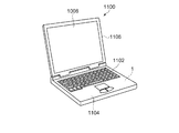
図7は、本発明の第1実施形態に係る電子モジュールを備える電子機器としてのモバイル型(又はノート型)のパーソナルコンピューターの構成の概略を示す斜視図である。この図において、パーソナルコンピューター1100は、キーボード1102を備えた本体部1104と、表示部1008を備えた表示ユニット1106とにより構成され、表示ユニット1106は、本体部1104に対しヒンジ構造部を介して屈折可能に支持されている。このようなパーソナルコンピューター1100には、その傾きなどを検出するためのジャイロセンサー等として機能する電子モジュール1が内蔵されている。パーソナルコンピューター1100から電磁的ノイズが発せられる場合でも、上述した電磁的ノイズの影響を受け難くい電子モジュール1を適用することで、傾き等の姿勢を安定して検出することができる。
FIG. 7 is a perspective view schematically illustrating the configuration of a mobile (or notebook) personal computer as an electronic apparatus including the electronic module according to the first embodiment of the present invention. In this figure, a
図8は、本発明の第1実施形態に係る電子モジュールを備える電子機器としての携帯電話機(PHSも含む)の構成の概略を示す斜視図である。この図において、携帯電話機1200は、複数の操作ボタン1202、受話口1204及び送話口1206を備え、操作ボタン1202と受話口1204との間には、表示部1208が配置されている。このような携帯電話機1200には、携帯電話機1200の傾きや、移動方向を検出するジャイロセンサー等として機能する電子モジュール1が内蔵されている。
携帯電話機1200から通信に伴う電磁波が発せられても、上述した電磁的ノイズ(電磁波)の影響を受け難くい電子モジュール1を適用することで、移動方向等を安定して検出することができる。
FIG. 8 is a perspective view schematically showing the configuration of a mobile phone (including PHS) as an electronic device including the electronic module according to the first embodiment of the present invention. In this figure, a
Even when an electromagnetic wave accompanying communication is emitted from the
図9は、本発明の第1実施形態に係る電子モジュールを備える電子機器としてのデジタルスチールカメラの構成の概略を示す斜視図である。なお、この図には、外部機器との接続についても簡易的に示されている。ここで、通常のカメラは、被写体の光像により銀塩写真フィルムを感光するのに対し、デジタルスチールカメラ1300は、被写体の光像をCCD(Charge Coupled Device)等の撮像素子により光電変換して撮像信号(画像信号)を生成する。
デジタルスチールカメラ1300におけるケース(ボディー)1302の背面には、表示部1308が設けられ、CCDによる撮像信号に基づいて表示を行う構成になっており、表示部1308は、被写体を電子画像として表示するファインダーとして機能する。また、ケース1302の正面側(図中裏面側)には、光学レンズ(撮像光学系)やCCD等を含む受光ユニット1304が設けられている。
撮影者が表示部1308に表示された被写体像を確認し、シャッターボタン1306を押下すると、その時点におけるCCDの撮像信号が、メモリー1310に転送・格納される。また、このデジタルスチールカメラ1300においては、ケース1302の側面に、ビデオ信号出力端子1312と、データ通信用の入出力端子1314とが設けられている。そして、図示されるように、ビデオ信号出力端子1312にはテレビモニター1430が、データ通信用の入出力端子1314にはパーソナルコンピューター1440が、それぞれ必要に応じて接続される。さらに、所定の操作により、メモリー1310に格納された撮像信号が、テレビモニター1430や、パーソナルコンピューター1440に出力される構成になっている。このようなデジタルスチールカメラ1300には、その傾きを検知するジャイロセンサー等として機能する電子モジュール1が内蔵されている。
デジタルスチールカメラ1300の動作に伴って光電変換を行うデジタル回路から電磁的ノイズが発せられても、上述した電磁的ノイズの影響を受け難くい電子モジュール1を適用することで、傾き等の姿勢を安定して検出することができる。
FIG. 9 is a perspective view schematically illustrating a configuration of a digital still camera as an electronic apparatus including the electronic module according to the first embodiment of the present invention. In this figure, connection with an external device is also simply shown. Here, an ordinary camera sensitizes a silver halide photographic film with a light image of a subject, whereas a
A
When the photographer confirms the subject image displayed on the
Even if electromagnetic noise is emitted from a digital circuit that performs photoelectric conversion in accordance with the operation of the
なお、本発明の第1実施形態に係る電子モジュール1は、図7のパーソナルコンピューター(モバイル型パーソナルコンピューター)、図8の携帯電話機、図9のデジタルスチールカメラの他にも、例えば、インクジェット式吐出装置(例えばインクジェットプリンター)、ラップトップ型パーソナルコンピューター、テレビ、ビデオカメラ、ビデオテープレコーダー、カーナビゲーション装置、ページャー、電子手帳(通信機能付も含む)、電子辞書、電卓、電子ゲーム機器、ワードプロセッサー、ワークステーション、テレビ電話、防犯用テレビモニター、電子双眼鏡、POS端末、医療機器(例えば電子体温計、血圧計、血糖計、心電図計測装置、超音波診断装置、電子内視鏡)、魚群探知機、各種測定機器、計器類(例えば、車両、航空機、船舶の計器類)、フライトシミュレーター等の電子機器に適用することができる。 The electronic module 1 according to the first embodiment of the present invention is not limited to the personal computer shown in FIG. 7 (mobile personal computer), the mobile phone shown in FIG. 8, and the digital still camera shown in FIG. Device (for example, inkjet printer), laptop personal computer, TV, video camera, video tape recorder, car navigation device, pager, electronic notebook (including communication function), electronic dictionary, calculator, electronic game device, word processor, work Station, video phone, security TV monitor, electronic binoculars, POS terminal, medical equipment (eg electronic thermometer, blood pressure monitor, blood glucose meter, electrocardiogram measuring device, ultrasonic diagnostic device, electronic endoscope), fish detector, various measurements Equipment, instruments (eg, vehicles, Sky machine, gauges of a ship), can be applied to electronic equipment such as a flight simulator.
[移動体]
図10は移動体の一例としての自動車を概略的に示す斜視図である。自動車1500には本発明に係る電子モジュール1が搭載されている。例えば、同図に示すように、移動体としての自動車1500には、電子モジュール1を内蔵して自動車1500の傾き等を制御する電子制御ユニット1508が車体1507に搭載されている。多数の電子制御ユニット1508が搭載される自動車1500等の移動体に振動と温度変化に強い当該電子モジュール1を用いることで、その電子制御ユニット1508の搭載位置の自由度を高めることができる。また、電子モジュール1は、他にも、カーナビゲーションシステム、アンチロックブレーキシステム(ABS)、エアバック、エンジンコントロール等の電子制御ユニット(ECU:electronic control unit)に広く適用できる。
[Moving object]
FIG. 10 is a perspective view schematically showing an automobile as an example of a moving body. The
1…電子モジュール、2…実装基板、3…支持部、4…電子部品、5…振動片、6…筐体、7…台座、10…蓋体、21…第1基板、22…第2基板、23…第3基板、24…第4基板、26…接続部、31a…上面、31b…下面、32,33,34,35…側面、40…回路素子、40a…第1回路部、40d…第2回路部、50…コネクター、60…シールド層、411…第1センサー素子、412…第2センサー素子、413…第3センサー素子、1100…パーソナルコンピューター、1200…携帯電話機、1300…デジタルスチールカメラ、1500…自動車。
DESCRIPTION OF SYMBOLS 1 ... Electronic module, 2 ... Mounting board, 3 ... Support part, 4 ... Electronic component, 5 ... Vibrating piece, 6 ... Case, 7 ... Base, 10 ... Cover, 21 ... 1st board | substrate, 22 ... 2nd board | substrate , 23 ... third substrate, 24 ... fourth substrate, 26 ... connection portion, 31a ... upper surface, 31b ... lower surface, 32, 33, 34, 35 ... side surface, 40 ... circuit element, 40a ... first circuit portion, 40d ... 2nd circuit part, 50 ... connector, 60 ... shield layer, 411 ... 1st sensor element, 412 ... 2nd sensor element, 413 ... 3rd sensor element, 1100 ... personal computer, 1200 ... mobile phone, 1300 ... digital
Claims (9)
第2のセンサー素子が設けられた第2の基板と、
前記第1の基板及び前記第2の基板を接続する接続部と、を備え、
前記第1の基板には、前記第1のセンサー素子と前記回路素子との間にシールド層が設けられていることを特徴とする電子モジュール。 A first substrate having a first surface provided with a first sensor element and a second surface provided with a circuit element;
A second substrate provided with a second sensor element;
A connecting portion for connecting the first substrate and the second substrate,
The electronic module according to claim 1, wherein a shield layer is provided between the first sensor element and the circuit element on the first substrate.
前記第1の基板及び前記第2の基板は、前記固定面の各々に固定されていることを特徴とする電子モジュール。 Having a support portion with a plurality of fixing surfaces;
The electronic module, wherein the first substrate and the second substrate are fixed to each of the fixed surfaces.
前記回路素子は前記台座に固定されている請求項4に記載の電子モジュール。 A pedestal for fixing the support portion;
The electronic module according to claim 4, wherein the circuit element is fixed to the pedestal.
前記第1回路部と前記第2回路部との間には分離層が設けられていることを特徴とする請求項1ないし請求項5のいずれか一項に記載の電子モジュール。 The circuit element includes a first circuit unit provided on the second surface, and a second circuit unit provided on the first circuit unit,
The electronic module according to claim 1, wherein a separation layer is provided between the first circuit portion and the second circuit portion.
前記第2回路部には、前記アナログ回路で増幅された出力信号をデジタル信号に変換するデジタル回路を含む、請求項6に記載の電子モジュール。 The first circuit unit includes an analog circuit that amplifies output signals of the first sensor element and the second sensor element,
The electronic module according to claim 6, wherein the second circuit unit includes a digital circuit that converts an output signal amplified by the analog circuit into a digital signal.
Priority Applications (2)
| Application Number | Priority Date | Filing Date | Title |
|---|---|---|---|
| JP2012189631A JP2014048090A (en) | 2012-08-30 | 2012-08-30 | Electronic module, electronic apparatus, and movable body |
| US14/013,772 US20140063753A1 (en) | 2012-08-30 | 2013-08-29 | Electronic module, electronic device, and mobile unit |
Applications Claiming Priority (1)
| Application Number | Priority Date | Filing Date | Title |
|---|---|---|---|
| JP2012189631A JP2014048090A (en) | 2012-08-30 | 2012-08-30 | Electronic module, electronic apparatus, and movable body |
Publications (2)
| Publication Number | Publication Date |
|---|---|
| JP2014048090A true JP2014048090A (en) | 2014-03-17 |
| JP2014048090A5 JP2014048090A5 (en) | 2015-10-08 |
Family
ID=50187315
Family Applications (1)
| Application Number | Title | Priority Date | Filing Date |
|---|---|---|---|
| JP2012189631A Withdrawn JP2014048090A (en) | 2012-08-30 | 2012-08-30 | Electronic module, electronic apparatus, and movable body |
Country Status (2)
| Country | Link |
|---|---|
| US (1) | US20140063753A1 (en) |
| JP (1) | JP2014048090A (en) |
Cited By (1)
| Publication number | Priority date | Publication date | Assignee | Title |
|---|---|---|---|---|
| US10866260B2 (en) | 2017-03-24 | 2020-12-15 | Seiko Epson Corporation | Physical quantity sensor, electronic apparatus, and vehicle |
Families Citing this family (4)
| Publication number | Priority date | Publication date | Assignee | Title |
|---|---|---|---|---|
| US9730340B1 (en) * | 2014-09-30 | 2017-08-08 | Apple Inc. | Electronic device with array of rotationally mounted components |
| US10187977B2 (en) | 2015-06-29 | 2019-01-22 | Microsoft Technology Licensing, Llc | Head mounted computing device, adhesive joint system and method |
| US10869393B2 (en) * | 2015-06-29 | 2020-12-15 | Microsoft Technology Licensing, Llc | Pedestal mounting of sensor system |
| CN116068026A (en) * | 2017-07-28 | 2023-05-05 | 京瓷株式会社 | Sensor element |
Citations (7)
| Publication number | Priority date | Publication date | Assignee | Title |
|---|---|---|---|---|
| JPH04176162A (en) * | 1990-11-07 | 1992-06-23 | Mitsubishi Electric Corp | Semiconductor integrated circuit device |
| JPH07306047A (en) * | 1994-05-10 | 1995-11-21 | Murata Mfg Co Ltd | Multi-axial detection type vibration gyro |
| JP2003329443A (en) * | 2002-05-14 | 2003-11-19 | Alps Electric Co Ltd | Detecting device |
| JP2005129888A (en) * | 2003-10-03 | 2005-05-19 | Matsushita Electric Works Ltd | Sensor device and sensor system, and manufacturing method therefor |
| JP2006308543A (en) * | 2005-03-31 | 2006-11-09 | Fujitsu Media Device Kk | Angular velocity sensor |
| JP2008541087A (en) * | 2005-05-10 | 2008-11-20 | センサータ テクノロジーズ ホランド ビー ヴイ | Sensor module package |
| WO2011140804A1 (en) * | 2010-08-09 | 2011-11-17 | Wang Tao | Micro inertial measurement system |
Family Cites Families (14)
| Publication number | Priority date | Publication date | Assignee | Title |
|---|---|---|---|---|
| DE10134620A1 (en) * | 2001-07-17 | 2003-02-06 | Bosch Gmbh Robert | Multi-axial inertial sensor system has sensor chips associated with sensor axes fixed on wafer plane on several rigid circuit substrates aligned according to sensor axis |
| US6918297B2 (en) * | 2003-02-28 | 2005-07-19 | Honeywell International, Inc. | Miniature 3-dimensional package for MEMS sensors |
| US7040922B2 (en) * | 2003-06-05 | 2006-05-09 | Analog Devices, Inc. | Multi-surface mounting member and electronic device |
| US7370530B2 (en) * | 2004-09-01 | 2008-05-13 | Honeywell International Inc. | Package for MEMS devices |
| SE528404C2 (en) * | 2004-10-20 | 2006-11-07 | Imego Ab | The sensor arrangement |
| EP1872087A4 (en) * | 2005-04-19 | 2012-10-17 | Jaymart Sensors Llc | Miniaturized inertial measurement unit and associated methods |
| US7467552B2 (en) * | 2005-11-10 | 2008-12-23 | Honeywell International Inc. | Miniature package for translation of sensor sense axis |
| US7536909B2 (en) * | 2006-01-20 | 2009-05-26 | Memsic, Inc. | Three-dimensional multi-chips and tri-axial sensors and methods of manufacturing the same |
| CN101416302A (en) * | 2006-04-07 | 2009-04-22 | 皇家飞利浦电子股份有限公司 | Elastically deformable integrated-circuit device |
| US20090056446A1 (en) * | 2007-09-05 | 2009-03-05 | Cluff Charles A | Multiple-axis sensor package and method of assembly |
| US8100010B2 (en) * | 2008-04-14 | 2012-01-24 | Honeywell International Inc. | Method and system for forming an electronic assembly having inertial sensors mounted thereto |
| US8037754B2 (en) * | 2008-06-12 | 2011-10-18 | Rosemount Aerospace Inc. | Integrated inertial measurement system and methods of constructing the same |
| US8194409B2 (en) * | 2009-11-09 | 2012-06-05 | Tyco Electronics Corporation | Guide frame for a pluggable module |
| JP5845672B2 (en) * | 2011-07-13 | 2016-01-20 | セイコーエプソン株式会社 | Sensor devices and electronics |
-
2012
- 2012-08-30 JP JP2012189631A patent/JP2014048090A/en not_active Withdrawn
-
2013
- 2013-08-29 US US14/013,772 patent/US20140063753A1/en not_active Abandoned
Patent Citations (7)
| Publication number | Priority date | Publication date | Assignee | Title |
|---|---|---|---|---|
| JPH04176162A (en) * | 1990-11-07 | 1992-06-23 | Mitsubishi Electric Corp | Semiconductor integrated circuit device |
| JPH07306047A (en) * | 1994-05-10 | 1995-11-21 | Murata Mfg Co Ltd | Multi-axial detection type vibration gyro |
| JP2003329443A (en) * | 2002-05-14 | 2003-11-19 | Alps Electric Co Ltd | Detecting device |
| JP2005129888A (en) * | 2003-10-03 | 2005-05-19 | Matsushita Electric Works Ltd | Sensor device and sensor system, and manufacturing method therefor |
| JP2006308543A (en) * | 2005-03-31 | 2006-11-09 | Fujitsu Media Device Kk | Angular velocity sensor |
| JP2008541087A (en) * | 2005-05-10 | 2008-11-20 | センサータ テクノロジーズ ホランド ビー ヴイ | Sensor module package |
| WO2011140804A1 (en) * | 2010-08-09 | 2011-11-17 | Wang Tao | Micro inertial measurement system |
Cited By (1)
| Publication number | Priority date | Publication date | Assignee | Title |
|---|---|---|---|---|
| US10866260B2 (en) | 2017-03-24 | 2020-12-15 | Seiko Epson Corporation | Physical quantity sensor, electronic apparatus, and vehicle |
Also Published As
| Publication number | Publication date |
|---|---|
| US20140063753A1 (en) | 2014-03-06 |
Similar Documents
| Publication | Publication Date | Title |
|---|---|---|
| US9470711B2 (en) | Physical quantity sensor and electronic apparatus | |
| JP6572603B2 (en) | Physical quantity sensor, electronic device and mobile object | |
| JP2014048090A (en) | Electronic module, electronic apparatus, and movable body | |
| JP2017125753A (en) | Electronic device, electronic apparatus, and moving body | |
| JP2014126495A (en) | Sensor, electronic apparatus, and moving body | |
| CN111669127A (en) | Vibration device, electronic apparatus, and moving object | |
| US20140035685A1 (en) | Resonator device, electronic device, electronic apparatus, and mobile object | |
| CN112311348B (en) | Vibration device, electronic apparatus, and moving object | |
| JP6167474B2 (en) | Sensor devices and electronics | |
| US20150114114A1 (en) | Angular velocity sensor, electronic apparatus, and moving object | |
| US11940275B2 (en) | Vibrator device, electronic apparatus, and vehicle | |
| JP6443058B2 (en) | Physical quantity sensor, electronic device and mobile object | |
| JP2015007561A (en) | Module, electronic device, and mobile body | |
| JP2017173074A (en) | Sensor device, electronic apparatus, and movable body | |
| JP6398730B2 (en) | PHYSICAL QUANTITY SENSOR, MANUFACTURING METHOD FOR PHYSICAL QUANTITY SENSOR, ELECTRONIC DEVICE, AND MOBILE BODY | |
| JP2016170002A (en) | Gyro module, electronic apparatus and mobile body | |
| JP2017151010A (en) | Sensor device, electronic equipment, and moving body | |
| JP2017126627A (en) | Electronic device, method for manufacturing the same, electronic equipment, and mobile body | |
| JP6303760B2 (en) | Functional elements, physical quantity sensors, electronic devices, and moving objects | |
| CN104579225A (en) | Vibrating element, vibrator, oscillator, electronic apparatus, and moving object | |
| JP2015099061A (en) | Manufacturing method of physical quantity detection device, vibration element, physical quantity detection device and electronic apparatus | |
| JP6488639B2 (en) | Electronic devices, electronic devices, and moving objects | |
| JP2016044977A (en) | Sensor element, sensor device, electronic equipment, and mobile body | |
| JP2014025742A (en) | Vibration piece, gyro sensor, electronic apparatus and movable body | |
| JP2016038306A (en) | Sensor element, sensor device, electronic equipment, and mobile body |
Legal Events
| Date | Code | Title | Description |
|---|---|---|---|
| RD04 | Notification of resignation of power of attorney |
Free format text: JAPANESE INTERMEDIATE CODE: A7424 Effective date: 20150108 |
|
| A521 | Request for written amendment filed |
Free format text: JAPANESE INTERMEDIATE CODE: A523 Effective date: 20150819 |
|
| A621 | Written request for application examination |
Free format text: JAPANESE INTERMEDIATE CODE: A621 Effective date: 20150819 |
|
| A977 | Report on retrieval |
Free format text: JAPANESE INTERMEDIATE CODE: A971007 Effective date: 20160526 |
|
| A131 | Notification of reasons for refusal |
Free format text: JAPANESE INTERMEDIATE CODE: A131 Effective date: 20160531 |
|
| RD04 | Notification of resignation of power of attorney |
Free format text: JAPANESE INTERMEDIATE CODE: A7424 Effective date: 20160610 |
|
| RD03 | Notification of appointment of power of attorney |
Free format text: JAPANESE INTERMEDIATE CODE: A7423 Effective date: 20160624 |
|
| A521 | Request for written amendment filed |
Free format text: JAPANESE INTERMEDIATE CODE: A523 Effective date: 20160726 |
|
| A131 | Notification of reasons for refusal |
Free format text: JAPANESE INTERMEDIATE CODE: A131 Effective date: 20161213 |
|
| A761 | Written withdrawal of application |
Free format text: JAPANESE INTERMEDIATE CODE: A761 Effective date: 20170203 |