JP6167474B2 - Sensor devices and electronics - Google Patents
Sensor devices and electronics Download PDFInfo
- Publication number
- JP6167474B2 JP6167474B2 JP2012090505A JP2012090505A JP6167474B2 JP 6167474 B2 JP6167474 B2 JP 6167474B2 JP 2012090505 A JP2012090505 A JP 2012090505A JP 2012090505 A JP2012090505 A JP 2012090505A JP 6167474 B2 JP6167474 B2 JP 6167474B2
- Authority
- JP
- Japan
- Prior art keywords
- terminal
- sensor
- detection
- sensor element
- chip
- Prior art date
- Legal status (The legal status is an assumption and is not a legal conclusion. Google has not performed a legal analysis and makes no representation as to the accuracy of the status listed.)
- Active
Links
Images


Description
本発明は、センサーデバイスおよび電子機器に関する。 The present invention relates to a sensor device and an electronic apparatus.
角速度、加速度等の物理量を検出するセンサーデバイスは、例えば、車両における車体制御、カーナビゲーションシステムの自車位置検出、デジタルカメラやビデオカメラ等の振動制御補正(いわゆる手ぶれ補正)等に用いられる。かかるセンサーデバイスとしては、例えば、振動ジャイロセンサーが知られている(例えば、特許文献1参照)。
例えば、特許文献1に記載の振動ジャイロセンサーは、駆動振動するとともに角速度が加わったときに検出振動が励振される振動片と、振動片を駆動振動させる駆動信号を出力するとともに振動片の検出振動に伴う検出信号を検出するICチップと、これらを収納するパッケージとを有する。
このような振動ジャイロセンサーにおいて、振動片およびICチップは、パッケージに設けられた複数の配線を介して互いに電気的に接続されている。これにより、ICチップから振動片へ駆動信号を供給するとともに、振動片からの検出信号をICチップで検出することができる。
Sensor devices that detect physical quantities such as angular velocity and acceleration are used, for example, for vehicle body control in vehicles, vehicle position detection in car navigation systems, vibration control correction (so-called camera shake correction) for digital cameras and video cameras, and the like. As such a sensor device, for example, a vibration gyro sensor is known (for example, see Patent Document 1).
For example, the vibration gyro sensor described in Patent Document 1 outputs a vibration piece that is driven to vibrate and detects vibration when an angular velocity is applied, and outputs a drive signal for driving and vibrating the vibration piece and detects vibration of the vibration piece. An IC chip for detecting a detection signal associated therewith, and a package for storing them.
In such a vibration gyro sensor, the resonator element and the IC chip are electrically connected to each other via a plurality of wirings provided in the package. Accordingly, it is possible to supply a drive signal from the IC chip to the vibrating piece and to detect a detection signal from the vibrating piece with the IC chip.
しかし、特許文献1に記載されているような従来のセンサーデバイスにおいては、駆動信号用の配線と検出信号用の配線とのいずれの配線もパッケージに設けられているため、これらの配線間の距離が短く、駆動信号用の配線から検出信号用の配線へのノイズの混入により、検出感度が低下するという問題があった。かかる問題は、センサーデバイスが小型になるほど、顕著となる。 However, in the conventional sensor device as described in Patent Document 1, since both the wiring for the drive signal and the wiring for the detection signal are provided in the package, the distance between these wirings However, there is a problem that the detection sensitivity is lowered due to the mixing of noise from the drive signal wiring to the detection signal wiring. Such a problem becomes more prominent as the sensor device becomes smaller.
本発明の目的は、優れた検出感度を有するセンサーデバイスを提供すること、さらに、かかるセンサーデバイスを備える信頼性に優れた電子機器を提供することにある。 The objective of this invention is providing the sensor device which has the outstanding detection sensitivity, and also providing the electronic device excellent in reliability provided with this sensor device.
本発明は、上述の課題の少なくとも一部を解決するためになされたものであり、以下の形態または適用例として実現することが可能である。
[適用例1]
本発明のセンサーデバイスは、駆動信号が入力される第1のセンサー端子と、検出信号を出力する第2のセンサー端子とを有し、前記第1のセンサー端子から入力された前記駆動信号により駆動振動されるとともに、物理量が加わったときに検出振動が励振され、前記検出振動に応じて前記検出信号を前記第2のセンサー端子から出力するセンサー素子と、
前記駆動信号を出力する第1のIC端子と、前記検出信号が入力される第2のIC端子とを有するICチップと、
前記センサー素子および前記ICチップが設置されるベースを有し、前記センサー素子および前記ICチップを収納するパッケージと、
前記ベースに設けられ、前記第1のセンサー端子と前記第1のIC端子とを電気的に接続する配線と、
前記第2のセンサー端子と前記第2のIC端子とを電気的に接続するボンディングワイヤーを備え、
前記センサー素子および前記ICチップは、前記ベースを平面視したときに、互いに並んで配置され、
前記第2のセンサー端子は、前記第1のセンサー端子に対して前記ICチップ側に配置され、
前記第2のIC端子は、前記第1のIC端子に対して前記センサー素子側に配置されており、
前記ベースの前記センサー素子とは反対側に設けられ、前記ICチップに電気的に接続された外部端子を有し、
前記外部端子は、前記ベースを平面視したときに、前記第2のセンサー端子と重なる領域に配置され、前記ICチップを調整するための調整用端子であることを特徴とする。
SUMMARY An advantage of some aspects of the invention is to solve at least a part of the problems described above, and the invention can be implemented as the following forms or application examples.
[Application Example 1]
The sensor device of the present invention has a first sensor terminal to which a drive signal is input and a second sensor terminal to output a detection signal, and is driven by the drive signal input from the first sensor terminal. A sensor element that is vibrated and excited when a physical quantity is applied, and that outputs the detection signal from the second sensor terminal in response to the detected vibration;
An IC chip having a first IC terminal for outputting the drive signal and a second IC terminal for receiving the detection signal;
A package on which the sensor element and the IC chip are placed; and a package for housing the sensor element and the IC chip;
Wiring provided on the base and electrically connecting the first sensor terminal and the first IC terminal;
A bonding wire for electrically connecting the second sensor terminal and the second IC terminal;
The sensor element and the IC chip are arranged side by side when the base is viewed in plan view,
The second sensor terminal is disposed on the IC chip side with respect to the first sensor terminal,
The second IC terminal is disposed on the sensor element side with respect to the first IC terminal ,
An external terminal provided on the opposite side of the base from the sensor element and electrically connected to the IC chip;
The external terminal is disposed in a region overlapping with the second sensor terminal when the base is viewed in plan, and is an adjustment terminal for adjusting the IC chip .
このように構成されたセンサーデバイスによれば、第1のセンサー端子と第1のIC端子とを電気的に接続する配線(第1の配線)と、第2のセンサー端子と第2のIC端子とを電気的に接続するボンディングワイヤー(第2の配線)との間の距離を大きくすることができる。そのため、第1の配線から第2の配線へのノイズの混入を防止または抑制することができる。その結果、センサーデバイスの検出感度を優れたものとすることができる。
また、センサー素子およびICチップが配置されている場合、第2の配線の形成が容易となる。
また、第2の配線の長さを短くすることができる。その結果、第2の配線へのノイズの混入をより効果的に防止または抑制することができる。
また、このような外部端子が設けられている場合であっても、外部端子と第2の配線との間の距離を大きくすることができるので、外部端子と第2の配線との間の浮遊容量を低減することができる。その結果、外部端子から第2の配線へのノイズの混入を防止または抑制することができる。
また、調整用端子は、一般に、センサーデバイスを設置したとき、接地されないため、電位の安定性が低い。したがって、調整用端子と第2の配線との間の浮遊容量を低減することによる効果がより顕著となる。
According to the sensor device configured as described above, the wiring (first wiring) that electrically connects the first sensor terminal and the first IC terminal, the second sensor terminal, and the second IC terminal. Can be increased in distance to the bonding wire (second wiring) that is electrically connected to each other. Therefore, it is possible to prevent or suppress noise from being mixed into the second wiring from the first wiring. As a result, the detection sensitivity of the sensor device can be made excellent.
Further, when the sensor element and the IC chip are disposed, the second wiring can be easily formed.
In addition, the length of the second wiring can be shortened. As a result, it is possible to more effectively prevent or suppress the mixing of noise into the second wiring.
Further, even when such an external terminal is provided, the distance between the external terminal and the second wiring can be increased, so that floating between the external terminal and the second wiring is possible. The capacity can be reduced. As a result, mixing of noise from the external terminal to the second wiring can be prevented or suppressed.
In addition, the adjustment terminal is generally not grounded when the sensor device is installed, so that the potential stability is low. Therefore, the effect of reducing the stray capacitance between the adjustment terminal and the second wiring becomes more remarkable.
[適用例2]
本発明のセンサーデバイスでは、前記配線は、成膜により形成されたものであることが好ましい。
これにより、簡単かつ確実に、第2の配線に対して離間した第1の配線を形成することができる。
[Application Example 2 ]
In the sensor device of the present invention, it is preferable that the wiring is formed by film formation.
Thereby, the 1st wiring spaced apart with respect to the 2nd wiring can be formed easily and reliably.
[適用例3]
本発明のセンサーデバイスでは、前記センサー素子は、基部と、前記基部から延出された振動腕とを有することが好ましい。
このようなセンサー素子は、駆動信号の強度に対して検出信号の強度が著しく小さい。そのため、第1の配線から第2の配線へのノイズの混入を防止または抑制することによる効果がより顕著となる。
[適用例4]
本発明のセンサーデバイスでは、前記ベースには、貫通孔が設けられており、
前記貫通孔は、前記ICチップに対して前記センサー素子とは反対側に設けられていることが好ましい。
[適用例5]
本発明の電子機器は、本発明のセンサーデバイスを備えることを特徴とする。
これにより、信頼性に優れる電子機器を提供することができる。
[Application Example 3 ]
In the sensor device of the present invention, it is preferable that the sensor element has a base portion and a vibrating arm extending from the base portion.
In such a sensor element, the intensity of the detection signal is significantly smaller than the intensity of the drive signal. Therefore, the effect of preventing or suppressing the mixing of noise from the first wiring to the second wiring becomes more remarkable.
[Application Example 4]
In the sensor device of the present invention, the base is provided with a through hole,
The through hole is preferably provided on the side opposite to the sensor element with respect to the IC chip.
[Application Example 5 ]
An electronic apparatus according to the present invention includes the sensor device according to the present invention.
Thereby, an electronic device having excellent reliability can be provided.
以下、本発明のセンサーデバイスおよび電子機器を添付図面に示す実施形態に基づいて詳細に説明する。
(センサーデバイス)
図1は、本発明の実施形態に係るセンサーデバイスの概略構成を示す断面図、図2は、図1に示すセンサーデバイスの平面図、図3は、図1に示すセンサーデバイスのセンサー素子の平面図、図4(a)は、図3中のA−A線断面図、図4(b)は、図3中のB−B線断面図、図5は、図3に示すセンサー素子の駆動を説明するための平面図である。
Hereinafter, a sensor device and an electronic apparatus of the present invention will be described in detail based on embodiments shown in the accompanying drawings.
(Sensor device)
1 is a cross-sectional view showing a schematic configuration of a sensor device according to an embodiment of the present invention, FIG. 2 is a plan view of the sensor device shown in FIG. 1, and FIG. 3 is a plan view of a sensor element of the sensor device shown in FIG. 4A is a cross-sectional view taken along line AA in FIG. 3, FIG. 4B is a cross-sectional view taken along line BB in FIG. 3, and FIG. 5 is a drive of the sensor element shown in FIG. It is a top view for demonstrating.
なお、図1〜5では、説明の便宜上、互いに直交する3軸として、x軸、y軸およびz軸を図示しており、その図示した矢印の先端側を「+側」、基端側を「−側」とする。また、以下では、x軸に平行な方向を「x軸方向」と言い、y軸に平行な方向を「y軸方向」と言い、z軸に平行な方向を「z軸方向」と言い、+z側(図1中の上側)を「上」、−z側(図1中の下側)を「下」と言う。
図1および図2に示すセンサーデバイス1は、角速度を検出するジャイロセンサーである。このセンサーデバイス1は、センサー素子(振動片)2と、ICチップ3と、センサー素子2およびICチップ3を収納するパッケージ9とを有している。
1 to 5, for convenience of explanation, the x axis, the y axis, and the z axis are illustrated as three axes that are orthogonal to each other. The tip side of the illustrated arrow is “+ side”, and the base end side is illustrated. “− Side”. In the following, a direction parallel to the x-axis is referred to as “x-axis direction”, a direction parallel to the y-axis is referred to as “y-axis direction”, and a direction parallel to the z-axis is referred to as “z-axis direction”. The + z side (upper side in FIG. 1) is referred to as “upper”, and the −z side (lower side in FIG. 1) is referred to as “lower”.
A sensor device 1 shown in FIGS. 1 and 2 is a gyro sensor that detects angular velocity. The sensor device 1 includes a sensor element (vibration piece) 2, an
(センサー素子)
センサー素子2は、センサー素子2の主面(xy面)に対してz軸まわりの角速度を検出する「面外検出型」のセンサー素子(振動片)である。このセンサー素子2は、図3に示すように、複数の振動腕を有する振動体20と、振動体20の表面に設けられた複数の検出電極群41、42、複数の駆動電極群51〜54、および複数の端子61〜66とを備える。
(Sensor element)
The
以下、センサー素子2を構成する各部を順次詳細に説明する。
[振動片]
まず、振動体20について説明する。
振動体20は、図3に示すように、いわゆるダブルT型と呼ばれる構造を有する。
具体的に説明すると、振動体20は、基部21と、基部21を支持する支持部22と、基部21から延出した2つの検出用振動腕23、24および4つの駆動用振動腕25〜28とを有する。
Hereinafter, each part which comprises the
[Vibration piece]
First, the vibrating
As shown in FIG. 3, the vibrating
More specifically, the vibrating
基部21は、本体部211と、本体部211からx軸方向に沿って互いに反対側へ延出する1対の連結腕212、213とを有する。
支持部22は、パッケージ9に対して固定される1対の固定部221、222と、固定部221と基部21の本体部211とを連結する1対の梁部223、224と、固定部222と基部21の本体部211とを連結する1対の梁部225、226とを有する。
The
The
検出用振動腕23、24は、基部21の本体部211からy軸方向に沿って互いに反対側へ延出している。
駆動用振動腕25、26は、基部21の連結腕212の先端部からy軸方向に沿って互いに反対側へ延出している。
駆動用振動腕27、28は、基部21の連結腕213の先端部からy軸方向に沿って互いに反対方向へ延出している。
The
The
The
本実施形態では、検出用振動腕23の先端部には、基端部よりも幅が大きい錘部(ハンマーヘッド)231が設けられている。同様に、検出用振動腕24の先端部には、錘部241が設けられ、駆動用振動腕25の先端部には、錘部251が設けられ、駆動用振動腕26の先端部には、錘部261が設けられ、駆動用振動腕27の先端部には、錘部271が設けられ、駆動用振動腕28の先端部には、錘部281が設けられている。このような錘部を設けることにより、センサー素子2の検出感度を向上させることができる。
In this embodiment, a weight portion (hammer head) 231 having a width larger than that of the base end portion is provided at the distal end portion of the
本実施形態では、振動体20は、圧電体材料で構成されている。
かかる圧電体材料としては、例えば、水晶、タンタル酸リチウム、ニオブ酸リチウム、ホウ酸リチウム、チタン酸バリウム等が挙げられる。特に、振動体20を構成する圧電体材料としては水晶(Zカット板)が好ましい。水晶で振動体20を構成すると、振動体20の振動特性(特に周波数温度特性)を優れたものとすることができる。また、エッチングにより高い寸法精度で振動体20を形成することができる。
In the present embodiment, the vibrating
Examples of the piezoelectric material include crystal, lithium tantalate, lithium niobate, lithium borate, and barium titanate. In particular, the piezoelectric material constituting the vibrating
[駆動電極群]
次に、駆動電極群51〜54について説明する。
図3に示すように、駆動電極群51は、振動体20の駆動用振動腕25上に設けられている。また、駆動電極群52は、振動体20の駆動用振動腕26上に設けられている。また、駆動電極群53は、振動体20の駆動用振動腕27上に設けられている。また、駆動電極群54は、振動体20の駆動用振動腕28上に設けられている。
[Drive electrode group]
Next, the
As shown in FIG. 3, the
駆動電極群51は、通電により駆動用振動腕25をx軸方向に屈曲振動させるものである。同様に、駆動電極群52は、通電により駆動用振動腕26をx軸方向に屈曲振動させるものである。また、駆動電極群53は、通電により駆動用振動腕27をx軸方向に屈曲振動させるものである。また、駆動電極群54は、通電により駆動用振動腕28をx軸方向に屈曲振動させるものである。
The
以下、駆動電極群51について詳細に説明する。なお、駆動電極群52〜54については、駆動電極群51と同様であるため、その説明を省略する。
駆動電極群51は、図4(a)に示すように、駆動用振動腕25の上面に設けられた駆動電極511と、駆動用振動腕25の下面に設けられた駆動電極512と、駆動用振動腕25の一方(図4(a)中の右側)の側面に設けられた駆動電極513と、駆動用振動腕25の他方(図4(a)中の左側)の側面に設けられた駆動電極514とで構成されている。
Hereinafter, the
As shown in FIG. 4A, the
駆動電極511〜514は、それぞれ、例えば、金(Au)、金合金、白金(Pt)、アルミニウム(Al)、アルミニウム合金、銀(Ag)、銀合金、クロム(Cr)、クロム合金、銅(Cu)、モリブデン(Mo)、ニオブ(Nb)、タングステン(W)、鉄(Fe)、チタン(Ti)、コバルト(Co)、亜鉛(Zn)、ジルコニウム(Zr)等の金属材料や、ITO、ZnO等の透明電極材料により形成することができる。
The
中でも、駆動電極511〜514の構成材料としては、それぞれ、金を主材料とする金属(金、金合金)または白金を用いるのが好ましく、金を主材料とする金属(特に金)を用いるのがより好ましい。
Auは、導電性に優れ(電気抵抗が小さく)、酸化に対する耐性に優れているため、電極材料として好適である。また、AuはPtに比しエッチングにより容易にパターニングすることができる。
Among these, as the constituent material of the
Au is suitable as an electrode material because it has excellent conductivity (low electrical resistance) and excellent resistance to oxidation. Further, Au can be easily patterned by etching as compared with Pt.
また、駆動電極511〜514の平均厚さは、それぞれ、特に限定されないが、例えば、1〜300nm程度であるのが好ましく、10〜200nmであるのがより好ましい。これにより、駆動電極511〜514が駆動電極群51の駆動特性や駆動用振動腕25の振動特性に悪影響を与えるのを防止しつつ、前述したような駆動電極511〜514の導電性を優れたものとすることができる。
The average thicknesses of the
なお、駆動電極511〜514と駆動用振動腕25との間には、駆動電極511〜514が駆動用振動腕25から剥離するのを防止する機能を有する下地層が設けられていてもよい。かかる下地層は、例えば、Ti、Cr等で構成することができる。
このような駆動電極群51は、駆動電極511、512と駆動電極513、514との間に電圧が印加されることにより、駆動用振動腕25をx軸方向に屈曲振動させる。
A base layer having a function of preventing the
The
駆動電極511および駆動電極512は、それぞれ、図示しない配線を介して、図3に示す固定部221に設けられた端子61(駆動信号端子)に電気的に接続されている。また、駆動電極513および駆動電極514は、それぞれ、図示しない配線を介して、図3に示す固定部222に設けられた端子64(駆動接地端子)に電気的に接続されている。
同様に、駆動電極群52〜54は、それぞれ、図示しない配線を介して、端子61および端子64に電気的に接続されている。
Each of the
Similarly, each of the drive electrode groups 52 to 54 is electrically connected to the terminal 61 and the terminal 64 via a wiring (not shown).
[検出電極群]
次に、検出電極群41、42について説明する。
検出電極群41は、前述した振動体20の検出用振動腕23上に設けられている。また、検出電極群42は、振動体20の検出用振動腕24上に設けられている。
検出電極群41は、検出用振動腕23のx軸方向での屈曲振動(いわゆる面内振動)を検出するものである。同様に、検出電極群42は、検出用振動腕24のx軸方向での屈曲振動を検出するものである。
[Detection electrode group]
Next, the
The
The
以下、検出電極群41について詳細に説明する。なお、検出電極群42については、検出電極群41と同様であるため、その説明を省略する。
検出電極群41は、図4(b)に示すように、検出用振動腕23の上面に設けられた検出電極411と、検出用振動腕23の下面に設けられた検出電極412と、検出用振動腕23の一方(図4(b)中の右側)の側面に設けられた検出電極413と、検出用振動腕23の他方(図4(b)中の左側)の側面に設けられた検出電極414とで構成されている。
Hereinafter, the
As shown in FIG. 4B, the
検出電極411〜414は、それぞれ、例えば、金(Au)、金合金、白金(Pt)、アルミニウム(Al)、アルミニウム合金、銀(Ag)、銀合金、クロム(Cr)、クロム合金、銅(Cu)、モリブデン(Mo)、ニオブ(Nb)、タングステン(W)、鉄(Fe)、チタン(Ti)、コバルト(Co)、亜鉛(Zn)、ジルコニウム(Zr)等の金属材料や、ITO、ZnO等の透明電極材料により形成することができる。
The
中でも、検出電極411〜414の構成材料としては、それぞれ、金を主材料とする金属(金、金合金)または白金を用いるのが好ましく、金を主材料とする金属(特に金)を用いるのがより好ましい。
Auは、導電性に優れ(電気抵抗が小さく)、酸化に対する耐性に優れているため、電極材料として好適である。また、AuはPtに比しエッチングにより容易にパターニングすることができる。
Among them, as a constituent material of the
Au is suitable as an electrode material because it has excellent conductivity (low electrical resistance) and excellent resistance to oxidation. Further, Au can be easily patterned by etching as compared with Pt.
また、検出電極411〜414の平均厚さは、それぞれ、特に限定されないが、例えば、1〜300nm程度であるのが好ましく、10〜200nmであるのがより好ましい。これにより、検出電極411〜414が検出電極群41の検出特性や検出用振動腕23の振動特性に悪影響を与えるのを防止しつつ、前述したような検出電極411〜414の導電性を優れたものとすることができる。
The average thickness of the
なお、検出電極411〜414と検出用振動腕23との間には、検出電極411〜414が検出用振動腕23から剥離するのを防止する機能を有する下地層が設けられていてもよい。かかる下地層は、例えば、Ti、Cr等で構成することができる。
このような検出電極群41は、検出用振動腕23のx軸方向での屈曲振動に伴って、検出電極411、412と検出電極413、414との間に電位差が生じる。
A base layer having a function of preventing the
In such a
検出電極411および検出電極412は、それぞれ、図示しない配線を介して、図3に示す固定部221に設けられた端子63(検出信号端子)に電気的に接続されている。また、検出電極413および検出電極414は、それぞれ、図示しない配線を介して、図3に示す固定部222に設けられた端子62(検出接地端子)に電気的に接続されている。
同様に、検出電極群42は、図示しない配線を介して、端子65(検出接地端子)および端子66(検出信号端子)に電気的に接続されている。
Each of the
Similarly, the detection electrode group 42 is electrically connected to a terminal 65 (detection ground terminal) and a terminal 66 (detection signal terminal) via a wiring (not shown).
[端子]
端子61〜63は、前述した支持部22の固定部221上に設けられ、端子64〜66は、支持部22の固定部222上に設けられている。
端子61は、前述したセンサー素子2の駆動電極群51〜54を駆動(すなわち駆動用振動腕25〜28を駆動振動)させる駆動信号が入力される駆動信号端子(第1のセンサー端子)である。これに対し、端子64は、端子61の電位に対して基準となる電位を有する駆動接地端子である。
[Terminal]
The
The terminal 61 is a driving signal terminal (first sensor terminal) to which a driving signal for driving the driving
また、端子63は、前述したセンサー素子2の検出電極群41からの検出信号を出力する検出信号端子(第2のセンサー端子)である。これに対し、端子62は、端子63の電位に対して基準となる電位を有する検出接地端子である。
同様に、端子66は、前述したセンサー素子2の検出電極群42からの検出信号を出力する検出信号端子(第2のセンサー端子)である。これに対し、端子65は、端子66の電位に対して基準となる電位を有する検出接地端子である。
The terminal 63 is a detection signal terminal (second sensor terminal) that outputs a detection signal from the
Similarly, the terminal 66 is a detection signal terminal (second sensor terminal) that outputs a detection signal from the detection electrode group 42 of the
検出信号端子である端子63、66は、それぞれ、駆動信号端子である端子61に対してICチップ3側に配置されている。これにより、ICチップ3からセンサー素子2へ検出信号を伝送する配線(後述する検出信号用の2つの配線70)の長さを短くすることができる。その結果、かかる配線へのノイズの混入をより効果的に防止または抑制することができる。
The
また、端子61〜66および配線(図示せず)等は、例えば、金(Au)、金合金、白金(Pt)、アルミニウム(Al)、アルミニウム合金、銀(Ag)、銀合金、クロム(Cr)、クロム合金、銅(Cu)、モリブデンン(Mo)、ニオブ(Nb)、タングステン(W)、鉄(Fe)、チタン(Ti)、コバルト(Co)、亜鉛(Zn)、ジルコニウム(Zr)等の金属材料やITO、ZnO等の透明電極材料により形成することができる。また、これらは、検出電極群41、42および駆動電極群51〜54と同時に一括形成することができる。
The
このように構成されたセンサー素子2は、次のようにしてz軸まわりの角速度ωを検出する。
まず、端子61と端子64との間に電圧(駆動信号)を印加することにより、図5(a)に示すように、図中矢印Aに示す方向に、駆動用振動腕25と駆動用振動腕27とを互いに接近・離間するように屈曲振動(駆動振動)させるとともに、駆動用振動腕26と駆動用振動腕28とを上記屈曲振動と同方向に互いに接近・離間するように屈曲振動(駆動振動)させる。
このとき、センサー素子2に角速度が加わらないと、駆動用振動腕25、26と駆動用振動腕27、28とは、中心点(重心G)を通るyz平面に対して面対称の振動を行っているため、基部21(本体部211および連結腕212、213)および検出用振動腕23、24は、ほとんど振動しない。
The
First, by applying a voltage (drive signal) between the terminal 61 and the terminal 64, as shown in FIG. 5A, the
At this time, if the angular velocity is not applied to the
このように駆動用振動腕25〜28を駆動振動させた状態で、センサー素子2にその重心Gを通る法線まわりの角速度ωが加わると、駆動用振動腕25〜28には、それぞれ、コリオリ力が働く。これにより、図5(b)に示すように、連結腕212、213を図中矢印Bに示す方向に屈曲振動し、これに伴い、この屈曲振動を打ち消すように、検出用振動腕23、24の図中矢印Cに示す方向の屈曲振動(検出振動)が励振される。
If the angular velocity ω around the normal line passing through the center of gravity G is applied to the
そして、検出用振動腕23の屈曲振動によって検出電極群41に生じた電荷が端子62、63から出力される。また、検出用振動腕24の屈曲振動によって検出電極群42に生じた電荷が端子65、66から出力される。
このように端子62、63、65、66から出力された電荷に基づいて、センサー素子2に加わった角速度ωを求めることができる。
Then, the charges generated in the
As described above, the angular velocity ω applied to the
(ICチップ3)
図1および図2に示すICチップ3は、前述したセンサー素子2を駆動する機能と、センサー素子2からの出力(センサー出力)を検出する機能とを有する電子部品である。
このようなICチップ3は、図示しないが、センサー素子2を駆動する駆動回路と、センサー素子2からの出力(電荷)を検出する検出回路とを備える。
(IC chip 3)
The
Although not shown, the
また、ICチップ3には、複数の接続端子31が設けられている。
複数の接続端子31は、前述したセンサー素子2を駆動する駆動信号を出力する1つの接続端子31b(第1のIC端子)と、センサー素子2からの検出信号が入力される2つの接続端子31a(第2のIC端子)とを含む。
2つの接続端子31aは、一方の接続端子31aが配線70を介してセンサー素子2の端子63に電気的に接続され、他方の接続端子31aが配線70を介してセンサー素子2の端子66に電気的に接続されている。
The
The plurality of
In the two
配線70は、一端部が端子63または端子66に固定されるとともに他端部が接続端子31aに固定されたボンディングワイヤーで構成されている。
一方、接続端子31bは、後述するパッケージ9のベース91に設けられた配線73を介して、センサー素子2の端子61に電気的に接続されている。
このように、配線70をボンディングワイヤーで構成し、かつ、配線73をベース91に設けることにより、検出信号用の配線70と駆動信号用の配線73とを間の距離を大きくすることができる。そのため、配線73から配線70へのノイズの混入を防止または抑制することができる。その結果、センサーデバイス1の検出感度を優れたものとすることができる。
特に、前述したような基部21、検出用振動腕23、24および駆動用振動腕25〜28を有するセンサー素子2は、駆動信号の強度に対して検出信号の強度が著しく小さい。そのため、配線73から配線70へのノイズの混入を防止または抑制することによる効果がより顕著となる。
The
On the other hand, the connection terminal 31b is electrically connected to the
As described above, the
In particular, in the
検出信号用の2つの接続端子31aは、それぞれ、駆動信号用の接続端子31bに対してセンサー素子2側に配置されている。これにより、ICチップ3からセンサー素子2へ検出信号を伝送する配線(後述する検出信号用の2つの配線70)の長さを短くすることができる。その結果、かかる配線へのノイズの混入をより効果的に防止または抑制することができる。
The two
(パッケージ)
パッケージ9は、センサー素子2およびICチップ3を収納するものである。
パッケージ9は、上面に開放する凹部を有するベース91と、ベース91の凹部の開口を塞ぐようにベース91に接合部材93(シールリング)を介して接合されたリッド(蓋体)92とを有している。このようなパッケージ9は、その内側に収納空間Sを有しており、この収納空間S内に、センサー素子2およびICチップ3が気密的に収納、設置されている。
(package)
The
The
ベース91は、センサー素子2およびICチップ3が設置されるものである。
本実施形態では、図2に示すように、ベース91を平面視したときに、センサー素子2およびICチップ3がx軸方向に互いに並んで配置されている。
このようにセンサー素子2およびICチップ3が配置されている場合、センサー素子2からICチップ3へ検出信号を伝送する配線(後述する配線70)の形成が容易となる。
また、z軸方向におけるセンサー素子2の上面とICチップ3の上面との間の距離が短くなるように、センサー素子2およびICチップ3が配置されている。これにより、上述する配線70の形成が容易となる。
The
In the present embodiment, as shown in FIG. 2, when the
When the
In addition, the
ベース91は、平板状の基板911と、基板911の上面に接合された平板状の基板912と、基板912の上面に接合された枠状の基板913と、基板913の上面に接合された枠状の914とで構成されている。
このベース91では、基板912の上面の一部が基板913および基板914の開口部内に露出し、基板913の上面の一部が基板914の開口部内に露出している。すなわち、ベース91には、基板912の上面と基板913との間に形成された段差と、基板913の上面と基板914との間に形成された段差とを有する凹部が形成されている。
ベース91の構成材料(基板911〜914の各構成材料)としては、特に限定されないが、例えば、酸化アルミニウム等の各種セラミックスを用いることができる。
The
In the
Although it does not specifically limit as a constituent material (each constituent material of the board | substrates 911-914) of the
このようなベース91の基板913の上面には、複数の内部端子71および複数の内部端子72が設けられている。
この複数の内部端子71は、ダミー用の2つの内部端子71aと、駆動信号用の1つの内部端子71bとを含む。
内部端子71bは、ベース91に設けられた配線73を介して1つの内部端子72に電気的に接続されている。
A plurality of
The plurality of
The
この配線73は、センサー素子2の端子61(第1のセンサー端子)と、ICチップ3の接続端子31b(第1のIC端子)とを電気的に接続する。
また、配線73は、成膜により形成されたものである。これにより、簡単かつ確実に、配線70に対して離間した配線73を形成することができる。
また、2つの内部端子71aおよび1つの内部端子71bを除く他の3つの内部端子71も、ベース91に設けられた配線(図示せず)を介して、対応する3つの内部端子72に電気的に接続されている。
The
The
The other three
一方、2つの内部端子71aは、内部端子72に対して電気的に接続されていないダミー端子であり、センサー素子2をベース91に対して固定する際の安定性を高めるものである。
このような複数(6つ)の内部端子71には、それぞれ、固定部材81を介してセンサー素子2が固定されている。
On the other hand, the two
The
ここで、複数の内部端子71のうちの2つの内部端子71aを除く4つの内部端子71に対応する固定部材81は、例えば、半田、銀ペースト、導電性接着剤(樹脂材料中に金属粒子などの導電性フィラーを分散させた接着剤)等で構成されている。これにより、かかる4つの内部端子71が固定部材81を介してセンサー素子2の端子61、62、64、65に電気的に接続されている。
Here, the fixing
また、2つの内部端子71aに対応する2つの固定部材81(固定部材81a)は、例えば、半田、銀ペースト、導電性接着剤(樹脂材料中に金属粒子などの導電性フィラーを分散させた接着剤)等で構成されていてもよいが、エポキシ樹脂、アクリル樹脂等を含む非導電性の接着剤で構成されているのが好ましい。これにより、固定部材81aにノイズが混入することによる検出感度の低下を防止することができる。
The two fixing members 81 (fixing
複数の内部端子72には、例えばボンディングワイヤーで構成された配線を介して、前述したICチップ3の複数の接続端子31(2つの接続端子31aを除く)が電気的に接続されている。
なお、各接続端子31aは、前述したように、ボンディングワイヤーで構成された配線70を介して、センサー素子2の端子63または端子66に電気的に接続されている。
The plurality of connection terminals 31 (excluding the two
As described above, each
また、ベース91の基板912の上面には、例えばエポキシ樹脂、アクリル樹脂等を含んで構成された接着剤のような固定部材82により、前述したICチップ3が固定されている。これにより、ICチップ3がベース91に対して支持・固定されている。
また、ベース91の基板911の下面(センサー素子2とは反対側)には、センサーデバイス1が組み込まれる機器(外部機器)に実装される際に用いられる複数の外部端子74と、ICチップ3を調整するための外部端子75(調整用端子)とが設けられている。
Further, the above-described
A plurality of
外部端子75は、ベース91を平面視したときに、センサー素子2の端子63または端子66と重なる領域に配置されている。
このような外部端子75が設けられている場合であっても、外部端子75と前述した検出信号用の配線70との間の距離を大きくすることができるので、外部端子75と配線70との間の浮遊容量を低減することができる。その結果、外部端子75から配線70へのノイズの混入を防止または抑制することができる。
また、外部端子75は、ICチップ3を調整するための調整用端子であるので、一般に、センサーデバイス1を設置したとき、接地されないため、電位の安定性が低い。したがって、このような調整用端子である外部端子75と配線70との間の浮遊容量を低減することによる効果がより顕著となる。
The
Even when such an
Further, since the
この複数の外部端子74、75は、それぞれ、図示しない内部配線を介して、対応する内部端子72に電気的に接続されている。これにより、各外部端子74、75は、ICチップ3に電気的に接続されている。
このような各内部端子71、72および各外部端子74、75等は、それぞれ、例えば、タングステン(W)等のメタライズ層にニッケル(Ni)、金(Au)等の被膜をメッキ等により積層した金属被膜からなる。
Each of the plurality of
Each of the
このようなベース91には、接合部材93を介してリッド92が気密的に接合されている。これにより、パッケージ9内が気密封止されている。
このリッド92は、例えば、ベース91と同材料、または、コバール、42アロイ、ステンレス鋼等の金属で構成されている。
また、接合部材93は、例えば、コバール、42アロイ、ステンレス鋼等の金属で構成されている。
A
The
Moreover, the joining
ベース91とリッド92との接合方法としては、特に限定されないが、例えば、シーム溶接、レーザー溶接等の溶接方法等を用いることができる。
また、ベース91には、収納空間S内を減圧または不活性ガス封入する際に用いる貫通孔94が形成されている。この貫通孔94は、封止材95により封止されている。
例えば、収納空間S内を減圧する場合、まず、封止材95により封止される前の貫通孔94を介して収納空間S内の空気を除去し、その状態を維持したまま、次いで、封止材95となる金属ボールを貫通孔94内に載置し、この金属ボールをレーザーにより溶融させることにより封止材95を形成し、貫通孔94を封止する。
A method for joining the
Further, the
For example, when the inside of the storage space S is depressurized, first, the air in the storage space S is removed through the through
また、図1、2に示すように、貫通孔94は、ICチップ3に対してセンサー素子2とは反対側に形成されている。これにより、貫通孔94とセンサー素子2との間の距離を長くすることができる。そのため、前述したように貫通孔94を封止材95により封止する際に、レーザーによる熱やスプラッシュ(金属ボールからの金属粉の飛散)がセンサー素子2に悪影響を与えるのを防止することができる。
以上説明したような第1実施形態に係るセンサーデバイス1によれば、配線73と各配線70とを間の距離を大きくすることができる。そのため、配線73から各配線70へのノイズの混入を防止または抑制することができる。その結果、センサーデバイス1の検出感度を優れたものとすることができる。
As shown in FIGS. 1 and 2, the through
According to the sensor device 1 according to the first embodiment as described above, the distance between the
(電子機器)
以上説明したようなセンサーデバイスは、各種電子機器に組み込むことにより、信頼性に優れた電子機器を提供することができる。
以下、本発明の電子デバイスを備える電子機器の一例について、図6〜図8に基づき、詳細に説明する。
(Electronics)
The sensor device as described above can provide an electronic device with excellent reliability by being incorporated in various electronic devices.
Hereinafter, an example of an electronic apparatus including the electronic device of the present invention will be described in detail with reference to FIGS.
図6は、本発明の電子機器を適用したモバイル型(またはノート型)のパーソナルコンピュータの構成を示す斜視図である。
この図において、パーソナルコンピュータ1100は、キーボード1102を備えた本体部1104と、表示部100を備えた表示ユニット1106とにより構成され、表示ユニット1106は、本体部1104に対しヒンジ構造部を介して回動可能に支持されている。
このようなパーソナルコンピュータ1100には、ジャイロセンサーとして機能する前述したセンサーデバイス1が内蔵されている。
FIG. 6 is a perspective view showing the configuration of a mobile (or notebook) personal computer to which the electronic apparatus of the present invention is applied.
In this figure, a
Such a
図7は、本発明の電子機器を適用した携帯電話機(PHSも含む)の構成を示す斜視図である。
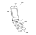
この図において、携帯電話機1200は、複数の操作ボタン1202、受話口1204および送話口1206を備え、操作ボタン1202と受話口1204との間には、表示部100が配置されている。
このような携帯電話機1200には、ジャイロセンサーとして機能する前述したセンサーデバイス1が内蔵されている。
FIG. 7 is a perspective view showing a configuration of a mobile phone (including PHS) to which the electronic apparatus of the present invention is applied.
In this figure, a
Such a
図8は、本発明の電子機器を適用したディジタルスチルカメラの構成を示す斜視図である。なお、この図には、外部機器との接続についても簡易的に示されている。
ここで、通常のカメラは、被写体の光像により銀塩写真フィルムを感光するのに対し、ディジタルスチルカメラ1300は、被写体の光像をCCD(Charge Coupled Device)などの撮像素子により光電変換して撮像信号(画像信号)を生成する。
FIG. 8 is a perspective view showing the configuration of a digital still camera to which the electronic apparatus of the present invention is applied. In this figure, connection with an external device is also simply shown.
Here, an ordinary camera sensitizes a silver halide photographic film with a light image of a subject, whereas a
ディジタルスチルカメラ1300におけるケース(ボディー)1302の背面には、表示部が設けられ、CCDによる撮像信号に基づいて表示を行う構成になっており、表示部は、被写体を電子画像として表示するファインダとして機能する。
また、ケース1302の正面側(図中裏面側)には、光学レンズ(撮像光学系)やCCDなどを含む受光ユニット1304が設けられている。
撮影者が表示部に表示された被写体像を確認し、シャッタボタン1306を押下すると、その時点におけるCCDの撮像信号が、メモリ1308に転送・格納される。
A display unit is provided on the back of a case (body) 1302 in the
A
When the photographer confirms the subject image displayed on the display unit and presses the
また、このディジタルスチルカメラ1300においては、ケース1302の側面に、ビデオ信号出力端子1312と、データ通信用の入出力端子1314とが設けられている。そして、図示されるように、ビデオ信号出力端子1312にはテレビモニタ1430が、データ通信用の入出力端子1314にはパーソナルコンピュータ1440が、それぞれ必要に応じて接続される。さらに、所定の操作により、メモリ1308に格納された撮像信号が、テレビモニタ1430や、パーソナルコンピュータ1440に出力される構成になっている。
このようなディジタルスチルカメラ1300には、ジャイロセンサーとして機能する前述したセンサーデバイス1が内蔵されている。
In the
Such a
なお、本発明の電子機器は、図6のパーソナルコンピュータ(モバイル型パーソナルコンピュータ)、図7の携帯電話機、図8のディジタルスチルカメラの他にも、電子デバイスの種類に応じて、例えば、車体姿勢検出装置、ポインティングデバイス、ヘッドマウントディスプレイ、インクジェット式吐出装置(例えばインクジェットプリンタ)、ラップトップ型パーソナルコンピュータ、テレビ、ビデオカメラ、ビデオテープレコーダ、ナビゲーション装置、ページャ、電子手帳(通信機能付も含む)、電子辞書、電卓、電子ゲーム機器、ゲームコントローラー、ワードプロセッサ、ワークステーション、テレビ電話、防犯用テレビモニタ、電子双眼鏡、POS端末、医療機器(例えば電子体温計、血圧計、血糖計、心電図計測装置、超音波診断装置、電子内視鏡)、魚群探知機、各種測定機器、計器類(例えば、車両、航空機、船舶の計器類)、フライトシュミレータ等に適用することができる。 In addition to the personal computer (mobile personal computer) shown in FIG. 6, the mobile phone shown in FIG. 7, and the digital still camera shown in FIG. Detection device, pointing device, head mounted display, ink jet type ejection device (for example, ink jet printer), laptop personal computer, television, video camera, video tape recorder, navigation device, pager, electronic notebook (including communication function), Electronic dictionary, calculator, electronic game device, game controller, word processor, workstation, videophone, TV monitor for crime prevention, electronic binoculars, POS terminal, medical device (eg electronic thermometer, blood pressure monitor, blood glucose meter, electrocardiogram measuring device, supersonic sound Diagnostic device, an electronic endoscope), a fish finder, various measurement devices, gauges (e.g., vehicle, aircraft, ship instruments), can be applied to a flight simulator or the like.
以上、本発明のセンサーデバイスおよび電子機器を図示の各実施形態に基づいて説明したが、本発明はこれらに限定されるものではなく、各部の構成は、同様の機能を有する任意の構成のものに置換することができる。また、他の任意の構成物が付加されていてもよい。また、本発明のセンサーデバイスは、前記各実施形態のうち、任意の2以上の構成(特徴)を組み合わせたものであってもよい。
また、前述した実施形態では、センサー素子が4つの駆動用振動腕および2つの検出用振動腕を備えるものを例に説明したが、これに限定されず、駆動用振動腕の数は、1〜3つまたは5つ以上であってもよく、また、検出用振動腕の数は、1つまたは3つ以上であってもよい。また、駆動用振動腕が検出用振動腕を兼ねていてもよい。
The sensor device and the electronic apparatus according to the present invention have been described based on the illustrated embodiments. However, the present invention is not limited to these embodiments, and the configuration of each unit is an arbitrary configuration having the same function. Can be substituted. Moreover, other arbitrary components may be added. In addition, the sensor device of the present invention may be a combination of any two or more configurations (features) of the above embodiments.
Further, in the above-described embodiment, the sensor element includes four driving vibration arms and two detection vibration arms. However, the embodiment is not limited thereto, and the number of driving vibration arms is 1 to 1. There may be three or five or more, and the number of detection vibrating arms may be one or three or more. The driving vibrating arm may also serve as the detecting vibrating arm.
また、前述した実施形態では、センサー素子の振動体が圧電体材料で構成されている場合を例に説明したが、センサー素子の振動体は、シリコン、石英等の非圧電体材料で構成されていてもよい。この場合、例えば、駆動用振動腕上および検出振動腕上にそれぞれ圧電体素子を設ければよい。また、この場合、シリコンで振動体を構成すると、優れた振動特性を有する振動体を比較的安価に実現することができる。また、公知の微細加工技術を用いてエッチングにより高い寸法精度で振動体を形成することができる。そのため、振動体の小型化を図ることができる。 In the above-described embodiment, the case where the vibration body of the sensor element is made of a piezoelectric material has been described as an example. However, the vibration body of the sensor element is made of a non-piezoelectric material such as silicon or quartz. May be. In this case, for example, a piezoelectric element may be provided on each of the driving vibration arm and the detection vibration arm. In this case, if the vibrating body is made of silicon, a vibrating body having excellent vibration characteristics can be realized at a relatively low cost. In addition, the vibrator can be formed with high dimensional accuracy by etching using a known fine processing technique. Therefore, the vibration body can be reduced in size.
1‥‥センサーデバイス 2‥‥センサー素子 3‥‥ICチップ 9‥‥パッケージ 20‥‥振動体 21‥‥基部 22‥‥支持部 23‥‥検出用振動腕 24‥‥検出用振動腕 25‥‥駆動用振動腕 26‥‥駆動用振動腕 27‥‥駆動用振動腕 28‥‥駆動用振動腕 31‥‥接続端子 31a‥‥接続端子 31b‥‥接続端子 41‥‥検出電極群 42‥‥検出電極群 51‥‥駆動電極群 52‥‥駆動電極群 53‥‥駆動電極群 54‥‥駆動電極群 61‥‥端子(第1のセンサー端子) 62‥‥端子 63‥‥端子(第2のセンサー端子) 64‥‥端子 65‥‥端子 66‥‥端子(第2のセンサー端子) 70‥‥配線(第2の配線) 71‥‥内部端子 71a‥‥内部端子 71b‥‥内部端子 72‥‥内部端子 73‥‥配線 74‥‥外部端子 75‥‥外部端子 81‥‥固定部材 81a‥‥固定部材 82‥‥固定部材 91‥‥ベース 92‥‥リッド 93‥‥接合部材 94‥‥貫通孔 95‥‥封止材 100‥‥表示部 211‥‥本体部 212‥‥連結腕 213‥‥連結腕 221‥‥固定部 222‥‥固定部 223‥‥梁部 224‥‥梁部 225‥‥梁部 226‥‥梁部 231‥‥錘部 241‥‥錘部 251‥‥錘部 261‥‥錘部 271‥‥錘部 281‥‥錘部 411‥‥検出電極 412‥‥検出電極 413‥‥検出電極 414‥‥検出電極 511‥‥駆動電極 512‥‥駆動電極 513‥‥駆動電極 514‥‥駆動電極 911‥‥基板 912‥‥基板 913‥‥基板 914‥‥基板 1100‥‥パーソナルコンピュータ 1102‥‥キーボード 1104‥‥本体部 1106‥‥表示ユニット 1200‥‥携帯電話機 1202‥‥操作ボタン 1204‥‥受話口 1206‥‥送話口 1300‥‥ディジタルスチルカメラ 1302‥‥ケース 1304‥‥受光ユニット 1306‥‥シャッタボタン 1308‥‥メモリ 1312‥‥ビデオ信号出力端子 1314‥‥入出力端子 1430‥‥テレビモニタ 1440‥‥パーソナルコンピュータ G‥‥重心 S‥‥収納空間 ω‥‥角速度
DESCRIPTION OF SYMBOLS 1 ...
Claims (5)
前記駆動信号を出力する第1のIC端子と、前記検出信号が入力される第2のIC端子とを有するICチップと、
前記センサー素子および前記ICチップが設置されるベースを有し、前記センサー素子および前記ICチップを収納するパッケージと、
前記ベースに設けられ、前記第1のセンサー端子と前記第1のIC端子とを電気的に接続する配線と、
前記第2のセンサー端子と前記第2のIC端子とを電気的に接続するボンディングワイヤーを備え、
前記センサー素子および前記ICチップは、前記ベースを平面視したときに、互いに並んで配置され、
前記第2のセンサー端子は、前記第1のセンサー端子に対して前記ICチップ側に配置され、
前記第2のIC端子は、前記第1のIC端子に対して前記センサー素子側に配置されており、
前記ベースの前記センサー素子とは反対側に設けられ、前記ICチップに電気的に接続された外部端子を有し、
前記外部端子は、前記ベースを平面視したときに、前記第2のセンサー端子と重なる領域に配置され、前記ICチップを調整するための調整用端子であることを特徴とするセンサーデバイス。 The first sensor terminal to which the drive signal is input and the second sensor terminal to output the detection signal are driven and vibrated by the drive signal input from the first sensor terminal, and the physical quantity is A sensor element that excites detection vibration when applied, and outputs the detection signal from the second sensor terminal in response to the detection vibration;
An IC chip having a first IC terminal for outputting the drive signal and a second IC terminal for receiving the detection signal;
A package on which the sensor element and the IC chip are placed; and a package for housing the sensor element and the IC chip;
Wiring provided on the base and electrically connecting the first sensor terminal and the first IC terminal;
A bonding wire for electrically connecting the second sensor terminal and the second IC terminal;
The sensor element and the IC chip are arranged side by side when the base is viewed in plan view,
The second sensor terminal is disposed on the IC chip side with respect to the first sensor terminal,
The second IC terminal is disposed on the sensor element side with respect to the first IC terminal ,
An external terminal provided on the opposite side of the base from the sensor element and electrically connected to the IC chip;
The external external terminal is an adjustment terminal for adjusting the IC chip, which is disposed in a region overlapping the second sensor terminal when the base is viewed in plan .
前記貫通孔は、前記ICチップに対して前記センサー素子とは反対側に設けられている請求項1ないし3のいずれかに記載のセンサーデバイス。 The sensor device according to claim 1, wherein the through hole is provided on the opposite side of the IC chip from the sensor element.
Priority Applications (1)
| Application Number | Priority Date | Filing Date | Title |
|---|---|---|---|
| JP2012090505A JP6167474B2 (en) | 2012-04-11 | 2012-04-11 | Sensor devices and electronics |
Applications Claiming Priority (1)
| Application Number | Priority Date | Filing Date | Title |
|---|---|---|---|
| JP2012090505A JP6167474B2 (en) | 2012-04-11 | 2012-04-11 | Sensor devices and electronics |
Publications (3)
| Publication Number | Publication Date |
|---|---|
| JP2013217856A JP2013217856A (en) | 2013-10-24 |
| JP2013217856A5 JP2013217856A5 (en) | 2015-05-28 |
| JP6167474B2 true JP6167474B2 (en) | 2017-07-26 |
Family
ID=49590101
Family Applications (1)
| Application Number | Title | Priority Date | Filing Date |
|---|---|---|---|
| JP2012090505A Active JP6167474B2 (en) | 2012-04-11 | 2012-04-11 | Sensor devices and electronics |
Country Status (1)
| Country | Link |
|---|---|
| JP (1) | JP6167474B2 (en) |
Families Citing this family (4)
| Publication number | Priority date | Publication date | Assignee | Title |
|---|---|---|---|---|
| JP6318556B2 (en) * | 2013-11-11 | 2018-05-09 | セイコーエプソン株式会社 | Package manufacturing method and electronic device manufacturing method |
| JP6372361B2 (en) * | 2015-01-16 | 2018-08-15 | 株式会社デンソー | Compound sensor |
| JP2016180612A (en) * | 2015-03-23 | 2016-10-13 | セイコーエプソン株式会社 | Vibration device, electronic apparatus, and mobile body |
| JP6572603B2 (en) * | 2015-04-13 | 2019-09-11 | セイコーエプソン株式会社 | Physical quantity sensor, electronic device and mobile object |
Family Cites Families (10)
| Publication number | Priority date | Publication date | Assignee | Title |
|---|---|---|---|---|
| JPH09148363A (en) * | 1995-11-22 | 1997-06-06 | Hitachi Ltd | Semiconductor device |
| JPH11340405A (en) * | 1998-05-22 | 1999-12-10 | Fujitsu Quantum Devices Kk | Lead frame, semiconductor device and manufacture thereof |
| JP4603135B2 (en) * | 2000-08-07 | 2010-12-22 | 住友精密工業株式会社 | Vibration type gyro sensor |
| US20040226373A1 (en) * | 2003-05-12 | 2004-11-18 | Hitachi Metals, Ltd. | Acceleration sensor device |
| US7555949B2 (en) * | 2004-04-07 | 2009-07-07 | Murata Manufacturing Co., Ltd. | Angular velocity measuring device |
| JP2007101531A (en) * | 2005-09-06 | 2007-04-19 | Seiko Instruments Inc | Dynamic amount sensor |
| JP2008096244A (en) * | 2006-10-11 | 2008-04-24 | Nippon Dempa Kogyo Co Ltd | Dual-axis detection type angular velocity sensor |
| JP5546132B2 (en) * | 2009-01-16 | 2014-07-09 | セイコーインスツル株式会社 | Electronic component package and method of manufacturing electronic component package |
| JP2010256332A (en) * | 2009-04-02 | 2010-11-11 | Seiko Epson Corp | Vibrating reed, vibrator, and physical quantity detector |
| JP2011082451A (en) * | 2009-10-09 | 2011-04-21 | Elpida Memory Inc | Package substrate for semiconductor and semiconductor device equipped with the same |
-
2012
- 2012-04-11 JP JP2012090505A patent/JP6167474B2/en active Active
Also Published As
| Publication number | Publication date |
|---|---|
| JP2013217856A (en) | 2013-10-24 |
Similar Documents
| Publication | Publication Date | Title |
|---|---|---|
| JP6318590B2 (en) | Vibration element, vibrator, vibration device, electronic device, and moving object | |
| JP6044101B2 (en) | SENSOR DEVICE, SENSOR DEVICE MANUFACTURING METHOD, AND ELECTRONIC DEVICE | |
| US10690500B2 (en) | Sensor element, sensor, electronic apparatus, and vehicle | |
| JP2015087262A (en) | Vibration element, vibrator, electronic apparatus and movable body | |
| JP6318550B2 (en) | Vibrating piece, angular velocity sensor, electronic device and moving object | |
| JP6167474B2 (en) | Sensor devices and electronics | |
| US9587944B2 (en) | Angular velocity sensor, electronic apparatus, and moving object | |
| US9123881B2 (en) | Electronic device and electronic apparatus | |
| US9048418B2 (en) | Sensor element, sensor device, and electronic apparatus | |
| US9599469B2 (en) | Angular velocity sensor, electronic apparatus, and moving object | |
| JP2018165642A (en) | Vibration device, electronic apparatus and moving body | |
| JP6507565B2 (en) | Electronic device, electronic device and mobile | |
| JP6413316B2 (en) | Manufacturing method of vibrating piece | |
| JP2015099061A (en) | Manufacturing method of physical quantity detection device, vibration element, physical quantity detection device and electronic apparatus | |
| JP2016170002A (en) | Gyro module, electronic apparatus and mobile body | |
| JP6492536B2 (en) | Sensor element, physical quantity sensor, electronic device and mobile object | |
| JP6488639B2 (en) | Electronic devices, electronic devices, and moving objects | |
| JP6939007B2 (en) | Sensors, electronics and mobiles | |
| JP6911446B2 (en) | Sensor elements, sensors, electronics and mobiles | |
| JP2016180612A (en) | Vibration device, electronic apparatus, and mobile body | |
| JP6492537B2 (en) | Sensor element, physical quantity sensor, electronic device and mobile object | |
| JP2016085178A (en) | Physical quantity detection vibration element, physical quantity sensor, electronic equipment and mobile body | |
| JP2016085185A (en) | Sensor element, physical quantity sensor, electronic apparatus and movable body | |
| JP2016044977A (en) | Sensor element, sensor device, electronic equipment, and mobile body | |
| JP2019152460A (en) | Vibration device, electronic device and moving object |
Legal Events
| Date | Code | Title | Description |
|---|---|---|---|
| A521 | Written amendment |
Free format text: JAPANESE INTERMEDIATE CODE: A523 Effective date: 20150406 |
|
| A621 | Written request for application examination |
Free format text: JAPANESE INTERMEDIATE CODE: A621 Effective date: 20150406 |
|
| A977 | Report on retrieval |
Free format text: JAPANESE INTERMEDIATE CODE: A971007 Effective date: 20160309 |
|
| A131 | Notification of reasons for refusal |
Free format text: JAPANESE INTERMEDIATE CODE: A131 Effective date: 20160315 |
|
| A521 | Written amendment |
Free format text: JAPANESE INTERMEDIATE CODE: A523 Effective date: 20160513 |
|
| A131 | Notification of reasons for refusal |
Free format text: JAPANESE INTERMEDIATE CODE: A131 Effective date: 20161018 |
|
| A521 | Written amendment |
Free format text: JAPANESE INTERMEDIATE CODE: A523 Effective date: 20161216 |
|
| TRDD | Decision of grant or rejection written | ||
| A01 | Written decision to grant a patent or to grant a registration (utility model) |
Free format text: JAPANESE INTERMEDIATE CODE: A01 Effective date: 20170530 |
|
| A61 | First payment of annual fees (during grant procedure) |
Free format text: JAPANESE INTERMEDIATE CODE: A61 Effective date: 20170612 |
|
| R150 | Certificate of patent or registration of utility model |
Ref document number: 6167474 Country of ref document: JP Free format text: JAPANESE INTERMEDIATE CODE: R150 |