EP1803836A1 - Evaporation source and method of depositing thin film using the same - Google Patents
Evaporation source and method of depositing thin film using the same Download PDFInfo
- Publication number
- EP1803836A1 EP1803836A1 EP06256598A EP06256598A EP1803836A1 EP 1803836 A1 EP1803836 A1 EP 1803836A1 EP 06256598 A EP06256598 A EP 06256598A EP 06256598 A EP06256598 A EP 06256598A EP 1803836 A1 EP1803836 A1 EP 1803836A1
- Authority
- EP
- European Patent Office
- Prior art keywords
- evaporation source
- crucible
- deposition
- baffle
- deposition material
- Prior art date
- Legal status (The legal status is an assumption and is not a legal conclusion. Google has not performed a legal analysis and makes no representation as to the accuracy of the status listed.)
- Granted
Links
- 238000000151 deposition Methods 0.000 title claims abstract description 93
- 238000001704 evaporation Methods 0.000 title claims abstract description 73
- 230000008020 evaporation Effects 0.000 title claims abstract description 70
- 239000010409 thin film Substances 0.000 title claims abstract description 20
- 238000000034 method Methods 0.000 title claims description 20
- 230000008021 deposition Effects 0.000 claims abstract description 84
- 239000000463 material Substances 0.000 claims abstract description 63
- 239000000758 substrate Substances 0.000 claims description 47
- 238000012545 processing Methods 0.000 claims description 29
- 238000010438 heat treatment Methods 0.000 claims description 19
- 239000007921 spray Substances 0.000 claims description 16
- 239000012530 fluid Substances 0.000 claims description 7
- 230000006698 induction Effects 0.000 claims description 6
- 238000005507 spraying Methods 0.000 claims description 5
- 238000004891 communication Methods 0.000 claims description 2
- 230000003213 activating effect Effects 0.000 claims 2
- 239000010408 film Substances 0.000 description 12
- 238000004519 manufacturing process Methods 0.000 description 3
- 239000002245 particle Substances 0.000 description 3
- 230000005855 radiation Effects 0.000 description 3
- 238000001771 vacuum deposition Methods 0.000 description 3
- PNEYBMLMFCGWSK-UHFFFAOYSA-N aluminium oxide Inorganic materials [O-2].[O-2].[O-2].[Al+3].[Al+3] PNEYBMLMFCGWSK-UHFFFAOYSA-N 0.000 description 2
- 238000005229 chemical vapour deposition Methods 0.000 description 2
- PMHQVHHXPFUNSP-UHFFFAOYSA-M copper(1+);methylsulfanylmethane;bromide Chemical compound Br[Cu].CSC PMHQVHHXPFUNSP-UHFFFAOYSA-M 0.000 description 2
- 230000003247 decreasing effect Effects 0.000 description 2
- 229910052751 metal Inorganic materials 0.000 description 2
- 239000002184 metal Substances 0.000 description 2
- 230000002093 peripheral effect Effects 0.000 description 2
- 238000005240 physical vapour deposition Methods 0.000 description 2
- 239000010936 titanium Substances 0.000 description 2
- 238000012546 transfer Methods 0.000 description 2
- PZNSFCLAULLKQX-UHFFFAOYSA-N Boron nitride Chemical compound N#B PZNSFCLAULLKQX-UHFFFAOYSA-N 0.000 description 1
- OKTJSMMVPCPJKN-UHFFFAOYSA-N Carbon Chemical compound [C] OKTJSMMVPCPJKN-UHFFFAOYSA-N 0.000 description 1
- RTAQQCXQSZGOHL-UHFFFAOYSA-N Titanium Chemical compound [Ti] RTAQQCXQSZGOHL-UHFFFAOYSA-N 0.000 description 1
- 230000015572 biosynthetic process Effects 0.000 description 1
- 229910052796 boron Inorganic materials 0.000 description 1
- 229910010293 ceramic material Inorganic materials 0.000 description 1
- 238000004581 coalescence Methods 0.000 description 1
- 239000000498 cooling water Substances 0.000 description 1
- 229910052593 corundum Inorganic materials 0.000 description 1
- 239000006185 dispersion Substances 0.000 description 1
- 238000009826 distribution Methods 0.000 description 1
- -1 e.g. Substances 0.000 description 1
- 229910002804 graphite Inorganic materials 0.000 description 1
- 239000010439 graphite Substances 0.000 description 1
- 239000012535 impurity Substances 0.000 description 1
- 238000007733 ion plating Methods 0.000 description 1
- 238000005259 measurement Methods 0.000 description 1
- 239000010453 quartz Substances 0.000 description 1
- 230000007261 regionalization Effects 0.000 description 1
- 239000004065 semiconductor Substances 0.000 description 1
- HBMJWWWQQXIZIP-UHFFFAOYSA-N silicon carbide Chemical compound [Si+]#[C-] HBMJWWWQQXIZIP-UHFFFAOYSA-N 0.000 description 1
- VYPSYNLAJGMNEJ-UHFFFAOYSA-N silicon dioxide Inorganic materials O=[Si]=O VYPSYNLAJGMNEJ-UHFFFAOYSA-N 0.000 description 1
- 238000004544 sputter deposition Methods 0.000 description 1
- 229910001220 stainless steel Inorganic materials 0.000 description 1
- 239000010935 stainless steel Substances 0.000 description 1
- 229910052719 titanium Inorganic materials 0.000 description 1
- 238000003466 welding Methods 0.000 description 1
- 229910001845 yogo sapphire Inorganic materials 0.000 description 1
Images

Classifications
-
- C—CHEMISTRY; METALLURGY
- C23—COATING METALLIC MATERIAL; COATING MATERIAL WITH METALLIC MATERIAL; CHEMICAL SURFACE TREATMENT; DIFFUSION TREATMENT OF METALLIC MATERIAL; COATING BY VACUUM EVAPORATION, BY SPUTTERING, BY ION IMPLANTATION OR BY CHEMICAL VAPOUR DEPOSITION, IN GENERAL; INHIBITING CORROSION OF METALLIC MATERIAL OR INCRUSTATION IN GENERAL
- C23C—COATING METALLIC MATERIAL; COATING MATERIAL WITH METALLIC MATERIAL; SURFACE TREATMENT OF METALLIC MATERIAL BY DIFFUSION INTO THE SURFACE, BY CHEMICAL CONVERSION OR SUBSTITUTION; COATING BY VACUUM EVAPORATION, BY SPUTTERING, BY ION IMPLANTATION OR BY CHEMICAL VAPOUR DEPOSITION, IN GENERAL
- C23C14/00—Coating by vacuum evaporation, by sputtering or by ion implantation of the coating forming material
- C23C14/06—Coating by vacuum evaporation, by sputtering or by ion implantation of the coating forming material characterised by the coating material
- C23C14/12—Organic material
-
- C—CHEMISTRY; METALLURGY
- C23—COATING METALLIC MATERIAL; COATING MATERIAL WITH METALLIC MATERIAL; CHEMICAL SURFACE TREATMENT; DIFFUSION TREATMENT OF METALLIC MATERIAL; COATING BY VACUUM EVAPORATION, BY SPUTTERING, BY ION IMPLANTATION OR BY CHEMICAL VAPOUR DEPOSITION, IN GENERAL; INHIBITING CORROSION OF METALLIC MATERIAL OR INCRUSTATION IN GENERAL
- C23C—COATING METALLIC MATERIAL; COATING MATERIAL WITH METALLIC MATERIAL; SURFACE TREATMENT OF METALLIC MATERIAL BY DIFFUSION INTO THE SURFACE, BY CHEMICAL CONVERSION OR SUBSTITUTION; COATING BY VACUUM EVAPORATION, BY SPUTTERING, BY ION IMPLANTATION OR BY CHEMICAL VAPOUR DEPOSITION, IN GENERAL
- C23C14/00—Coating by vacuum evaporation, by sputtering or by ion implantation of the coating forming material
- C23C14/22—Coating by vacuum evaporation, by sputtering or by ion implantation of the coating forming material characterised by the process of coating
- C23C14/24—Vacuum evaporation
- C23C14/243—Crucibles for source material
-
- C—CHEMISTRY; METALLURGY
- C23—COATING METALLIC MATERIAL; COATING MATERIAL WITH METALLIC MATERIAL; CHEMICAL SURFACE TREATMENT; DIFFUSION TREATMENT OF METALLIC MATERIAL; COATING BY VACUUM EVAPORATION, BY SPUTTERING, BY ION IMPLANTATION OR BY CHEMICAL VAPOUR DEPOSITION, IN GENERAL; INHIBITING CORROSION OF METALLIC MATERIAL OR INCRUSTATION IN GENERAL
- C23C—COATING METALLIC MATERIAL; COATING MATERIAL WITH METALLIC MATERIAL; SURFACE TREATMENT OF METALLIC MATERIAL BY DIFFUSION INTO THE SURFACE, BY CHEMICAL CONVERSION OR SUBSTITUTION; COATING BY VACUUM EVAPORATION, BY SPUTTERING, BY ION IMPLANTATION OR BY CHEMICAL VAPOUR DEPOSITION, IN GENERAL
- C23C14/00—Coating by vacuum evaporation, by sputtering or by ion implantation of the coating forming material
- C23C14/22—Coating by vacuum evaporation, by sputtering or by ion implantation of the coating forming material characterised by the process of coating
- C23C14/24—Vacuum evaporation
- C23C14/246—Replenishment of source material
-
- C—CHEMISTRY; METALLURGY
- C23—COATING METALLIC MATERIAL; COATING MATERIAL WITH METALLIC MATERIAL; CHEMICAL SURFACE TREATMENT; DIFFUSION TREATMENT OF METALLIC MATERIAL; COATING BY VACUUM EVAPORATION, BY SPUTTERING, BY ION IMPLANTATION OR BY CHEMICAL VAPOUR DEPOSITION, IN GENERAL; INHIBITING CORROSION OF METALLIC MATERIAL OR INCRUSTATION IN GENERAL
- C23C—COATING METALLIC MATERIAL; COATING MATERIAL WITH METALLIC MATERIAL; SURFACE TREATMENT OF METALLIC MATERIAL BY DIFFUSION INTO THE SURFACE, BY CHEMICAL CONVERSION OR SUBSTITUTION; COATING BY VACUUM EVAPORATION, BY SPUTTERING, BY ION IMPLANTATION OR BY CHEMICAL VAPOUR DEPOSITION, IN GENERAL
- C23C14/00—Coating by vacuum evaporation, by sputtering or by ion implantation of the coating forming material
- C23C14/22—Coating by vacuum evaporation, by sputtering or by ion implantation of the coating forming material characterised by the process of coating
- C23C14/24—Vacuum evaporation
- C23C14/26—Vacuum evaporation by resistance or inductive heating of the source
-
- C—CHEMISTRY; METALLURGY
- C23—COATING METALLIC MATERIAL; COATING MATERIAL WITH METALLIC MATERIAL; CHEMICAL SURFACE TREATMENT; DIFFUSION TREATMENT OF METALLIC MATERIAL; COATING BY VACUUM EVAPORATION, BY SPUTTERING, BY ION IMPLANTATION OR BY CHEMICAL VAPOUR DEPOSITION, IN GENERAL; INHIBITING CORROSION OF METALLIC MATERIAL OR INCRUSTATION IN GENERAL
- C23C—COATING METALLIC MATERIAL; COATING MATERIAL WITH METALLIC MATERIAL; SURFACE TREATMENT OF METALLIC MATERIAL BY DIFFUSION INTO THE SURFACE, BY CHEMICAL CONVERSION OR SUBSTITUTION; COATING BY VACUUM EVAPORATION, BY SPUTTERING, BY ION IMPLANTATION OR BY CHEMICAL VAPOUR DEPOSITION, IN GENERAL
- C23C14/00—Coating by vacuum evaporation, by sputtering or by ion implantation of the coating forming material
- C23C14/22—Coating by vacuum evaporation, by sputtering or by ion implantation of the coating forming material characterised by the process of coating
- C23C14/34—Sputtering
-
- C—CHEMISTRY; METALLURGY
- C23—COATING METALLIC MATERIAL; COATING MATERIAL WITH METALLIC MATERIAL; CHEMICAL SURFACE TREATMENT; DIFFUSION TREATMENT OF METALLIC MATERIAL; COATING BY VACUUM EVAPORATION, BY SPUTTERING, BY ION IMPLANTATION OR BY CHEMICAL VAPOUR DEPOSITION, IN GENERAL; INHIBITING CORROSION OF METALLIC MATERIAL OR INCRUSTATION IN GENERAL
- C23C—COATING METALLIC MATERIAL; COATING MATERIAL WITH METALLIC MATERIAL; SURFACE TREATMENT OF METALLIC MATERIAL BY DIFFUSION INTO THE SURFACE, BY CHEMICAL CONVERSION OR SUBSTITUTION; COATING BY VACUUM EVAPORATION, BY SPUTTERING, BY ION IMPLANTATION OR BY CHEMICAL VAPOUR DEPOSITION, IN GENERAL
- C23C16/00—Chemical coating by decomposition of gaseous compounds, without leaving reaction products of surface material in the coating, i.e. chemical vapour deposition [CVD] processes
-
- H01L21/203—
Definitions
- the present invention relates to an evaporation source and a method for depositing thin films using the same.
- the present invention relates to an evaporation source and method for depositing thin films capable of providing uniform film thickness and minimized heat radiation.
- thin films may be deposited in display devices, such as electroluminescent (EL) display devices, to provide photon-emitting mediums to form images.
- EL electroluminescent
- Such thin films may be applied to a substrate, e.g., an electrode, by methods such as physical vapor deposition (PVD), e.g., vacuum deposition, chemical vapor deposition (CVD), ion plating, sputtering, and so forth.
- PVD physical vapor deposition
- CVD chemical vapor deposition
- ion plating ion plating
- sputtering ion plating
- sputtering e.g., a substrate
- a vacuum environment e.g., vacuum chamber
- An evaporation source having a heating unit and a deposition material e.g., organic light-emitting material, may be either connected to the vacuum environment or installed therein, such that the operation of the evaporation source may evaporate the deposition material and form a thin film on the substrate.
- An evaporation source may include a crucible to contain a deposition material, a heating unit to heat the crucible and evaporate the deposition material, and at least one spray nozzle to apply the evaporated deposition material to a substrate.
- the particles of the evaporated deposition material may have a tendency to coalesce and form clusters of particles having various sizes, thereby providing an evaporated deposition material having non-uniform texture and density consistency. Further, such non-uniform evaporated deposition material may cause application of non-uniform layers of deposition material onto substrates, thereby producing films lacking uniform thickness.
- application of the evaporated deposition material through a conventional spray nozzle onto a substrate may radiate excess heat into a processing chamber, thereby deforming the substrate upon contact therewith.
- deposition material to a rotatable substrate may require a large size of a processing chamber in order to accommodate sufficient space for substrate movement. Such large substrates may also sag or collapse as a result of upward application of deposition material thereon.
- the present invention is therefore directed to an evaporation source and method of employing the same, which substantially overcome one or more of the disadvantages of the related art.
- the invention accordingly sets out to provide an evaporation source and a method employing the same having the capability of minimizing the coalescence of the evaporated deposition material, thereby improving uniformity of thin deposition layers.
- the invention also aims to provide an evaporation source and a method employing the same having a nozzle structure with improved heat radiation distribution, thereby minimizing excessive heat transfer into a processing chamber.
- a first aspect of the invention provides an evaporation source as set out in claim 1.
- Preferred features of this aspect of the invention are set out in claims 2 to 10.
- a second aspect of the invention provdes a method of depositing a thin film as set out in Claim 11. Preferred features of this aspect of the invention are set out in claims 12 to 16.
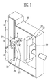
- FIG. 1 illustrates a perspective view of an apparatus for depositing a thin films using an evaporation source according to an embodiment of the present invention
- FIG. 2A illustrates a cross-sectional view of an evaporation source according to an embodiment of the present invention taken along the line I-I' of FIG. 1;
- FIG. 2B illustrates a cross-sectional view of a direction of movement of an evaporated deposition material inside an evaporation source according to an embodiment of the present invention taken along the line I-I' of FIG. 1;
- FIG. 3A illustrates a plan view of an evaporation source according to an embodiment of the present invention taken along the line II-II' of FIG. 1;
- FIG. 3B illustrates a plan view of a direction of movement of an evaporated deposition material inside an evaporation source having a shower head structure according to an embodiment of the present invention taken along the line II-II' of FIG. 1.
- an apparatus for depositing thin films includes a processing chamber 20, a supporting unit 23 for securing a substrate, an evaporation source 24, and a deposition rate measuring unit 26 coupled to the evaporation source 24.
- the processing chamber 20 of an embodiment of the present invention may be any type of vessel known by those skilled in the art for use in film processing, and, preferably, it may be a pressure-controlled vessel such as a vacuum chamber.
- the processing chamber 20 is in this case formed to have a deposition preventing part A and a film forming part B.
- the film forming part B refers to the central area of the processing chamber 20.
- the central area of the processing chamber 20 corresponds to a position where a substrate may be placed and formation of a film, e.g., vacuum deposition processing, may occur.
- the deposition preventing part A refers to the area inside the processing chamber 20 that surrounds the film forming part B. In other words, the deposition preventing part A is formed as peripheral portions of film forming part B.
- the peripheral portions, i.e., deposition preventing part A are excluded from film deposition processing.
- the deposition preventing part A may include a heat absorbing plate (not shown) formed around a substrate to remove excess heat from the substrate and provide uniform temperature and uniform film thickness.
- a substrate 21 and a mask 22 are in use, placed in the processing chamber 20.
- the substrate 21 and mask 22 are placed in the center of the processing chamber 20, i.e., film forming part B, such that the deposition preventing part A surrounds them.
- the mask 22 is attached to the substrate 21 between the substrate 21 and the evaporation source 24.
- the mask 22 may include a pattern formation unit (not shown) having a pattern corresponding to a pattern to be imparted to a thin film formed on the substrate 21, and a fixation unit (not shown) secured to a mask frame (not shown) through welding.
- the supporting unit 23 of this embodiment of the present invention is coupled to the processing chamber 20 in order to secure the substrate 21 and the mask 22 in the film forming part A of the processing chamber 20, as illustrated in FIG. 1.
- the supporting unit 23 is formed as a longitudinal member connected to the processing chamber 20 at one end and to a substrate at the other end, such that a substrate may be stably secured in its position. Additionally, an alignment system (not shown) may be added to align the substrate 21 and the mask thereon.
- the evaporation source 24 supplies sufficient heat to evaporate a deposition material placed therein, and, subsequently, apply it to a substrate in order to form a thin film.
- the detailed structure of the evaporation source 24 will be described in more detail with respect to FIGS. 2A-3B.
- the evaporation source 24 of this embodiment of the present invention includes a crucible 33 for storing a deposition material 37, a heating unit 32 for evaporating the deposition material 37, at least one spray nozzle 38 for spraying the deposition material 37 onto the substrate 21, and a baffle 34 inside the crucible 33.
- the above mentioned components are enclosed by a housing 30.
- the crucible 33 is formed to include a predetermined space for containing the deposition material 37 to be deposited onto the substrate 21, and it may be formed of any material known in the art that has excellent heat conductivity.
- the crucible 33 may be formed of a ceramic material, e.g., graphite, silicon carbide (SiC), aluminum nitride (AIN), alumina (Al 2 O 3 ), boron nitride (BN), quartz, and so forth, or of a metal, e.g., titanium (Ti), stainless steel, and so forth.
- the crucible 33 further includes a baffle 34.
- Other embodiments may have more than one baffle.
- the baffle 34 is formed inside the crucible 33 in a form of at least one longitudinal baffle plate, as illustrated in FIGS. 2A-2B.
- the baffle 34 is formed of any suitable material known in the art, and it may be positioned parallel to the predetermined space containing the deposition material 37 to divide the crucible into a plurality of channels 39, as further illustrated in FIGS. 2A-2B.
- the plurality of channels 39 include two channels that form a labyrinthine movement path for the evaporated deposition material 37 from the crucible 33 to the induction channel 35.
- FIG. 3A An embodiment including a plurality of baffle plates, (in this case three baffle plates 34A, 34B, and 34C), is shown in FIG. 3A.
- the baffle plates are arranged parallel to each other throughout the width of the crucible 33 in such a way that a labyrinth is formed along the path of movement of the evaporated deposition material 37.
- the deposition material 37 evaporates and flows from the crucible 33 through the baffle 34 and the plurality of channels 39 towards the induction channel 35.
- the flow of the evaporated deposition material 37 collides with the baffle 34 and, thereby, enhances break-up of any coalesced clusters of the evaporated deposition material 37.
- cluster break-up enhances the uniformity of the evaporated deposition material in terms of texture and density, i.e., the evaporated deposition material includes particles having substantially similar dimensions.
- the deposition material 37 may be any type of material employed in the art for forming thin films in display devices.
- the deposition material may be a light-emitting material or, more preferably, an organic light-emitting material.
- the heating unit 32 includes at least one heater (not shown).
- the evaporation source 24 includes two heating units 32, each heating unit 32 having at least one electrical heater (not shown). As such, the heating unit 32 may be formed in close proximity to the crucible 33 to provide sufficient heat to evaporate the deposition material 37 contained therein.
- One heating unit 32 is located on each horizontal side of the crucible 33, as illustrated in FIG. 2A.
- a reflector 31 is provided between each heating unit 32 and the housing 30 surrounding the crucible 33.
- the evaporation source 24 includes a plurality of reflectors 31 formed in close proximity to the heating units 32 to reflect heat emitted from the heating units 32 into the crucible 33, thereby minimizing heat leakage outside the evaporation source 24.
- the spray nozzle 38 is situated in the housing 30, and protrudes through the housing 30.
- the spray nozzle 38 is connected to an induction channel 35, which may then direct the deposition material 37 from the crucible 33 into the nozzle 38, as illustrated in FIG. 2B.
- the spray nozzle 38 may have a shower head structure, as illustrated in FIG. 3B.
- the spray nozzle 38 may include a plurality of nozzle orifices 40 formed through the housing 30, such that application of the evaporated deposition material 37 through the plurality of nozzle orifices 40 may be simultaneous and uniform.
- the plurality of nozzle orifices 40 may be in fluid communication with the deposition material 37 through a plurality of channels.
- the housing 30 may be formed to include a double wall having an internal wall (not shown) and an external wall (not shown).
- the double wall structure may provide sufficient space between the internal and external walls for cooling water to facilitate temperature control.
- the evaporation source 24 of the above described first embodiment of the present invention also includes an insulating plate 36 between the crucible 33 and the inside wall of the housing 30.
- the insulating plate 36 may minimize heat transfer from the induction channel 35 into the processing chamber 20 and the substrate 21.
- the evaporation source 24 is moveable.
- the evaporation source 24 is formed on a driving shaft 26.
- the driving shaft 26 is formed parallel to the longitudinal side of the substrate 21 inside the processing chamber 20.
- the driving shaft 26 includes a rotary unit (not shown) that may rotate and move the evaporation source 24 along the driving shaft 26, such that the evaporation unit 24 may move up and down along the driving shaft 26 in a direction perpendicular to the direction of the rotation of the driving shaft 26.
- a movable evaporation source 24 reduces the size of the processing chamber 20 by at least about 75% as compared to a size of a processing chamber having a stationary evaporation source and a rotatable substrate.
- the evaporation source 24 further includes a deposition rate measuring unit 25.
- the deposition rate measuring unit 25 is affixed to the evaporation source 24, such that the deposition rate measuring unit 25 and the evaporation source 24 may move jointly.
- the deposition rate measuring unit 25 may also be integral with the evaporation source 24.
- the joint motion of the deposition rate measuring unit 25 and the evaporation source 24, whether integrated or not, allows continuous real-time measurement of the evaporation rate of the deposition material and control of its deposition rate onto the substrate 21.
- the deposition rate measuring unit 25 may also have the capability of adjusting the evaporation rate of the deposition material in order to achieve a specific deposition rate onto a substrate.
- the deposition rate measuring unit 25 may be electrically connected to the heating unit 32 of the evaporation source 24, such that the heat amount generated for evaporating the deposition material 37 in the evaporation source 24 may be increased or decreased with respect to a desired deposition rate.
- the deposition rate measuring unit 25 may be electrically connected to the rotary unit of the driving shaft 26, such that the speed at which the evaporation source 24 moves may be increased or decreased with respect to the generated amount of the evaporated deposition material 37.
- the control of the evaporation source 24 speed may facilitate control of the exposure time of the substrate 21 to the evaporation source 24, i.e., deposition rate.
- a method of depositing a thin film onto a substrate in accordance with the invention is described below with reference to FIGS. 1-2B.
- the substrate 21 is placed in the processing chamber 20, and secured therein with the supporting unit 23.
- the mask 22 is attached to the surface of the substrate 21 to be coated.
- the evaporation source 24 is provided in the processing chamber 20, such that the evaporation source 24 faces the surface of the substrate 21 that is to be coated.
- a deposition material 37 e.g., a metal or a light-emitting material such as an organic light-emitting material employed in manufacturing of organic-light emitting diodes (OLEDs) is placed in the crucible 33 of the evaporation source 24.
- a deposition material 37 e.g., a metal or a light-emitting material such as an organic light-emitting material employed in manufacturing of organic-light emitting diodes (OLEDs)
- the heating unit 32 of the evaporation source 24 is activated to heat the crucible 33, such that the deposition material 37 placed therein is evaporated, e.g., gasified or sublimated.
- the evaporated deposition material 37 then passes around at least one baffle plate of the baffle 34 to form a uniform deposition fluid having substantially uniform texture and density, and the uniform deposition fluid continues through channels 39 into the induction channel 35, and, subsequently, into the spray nozzle 38.
- the evaporation temperatures in the evaporation source 24 are low, i.e., they range from about 200°C to about 400°C.
- the evaporated deposition material 37 is applied to the substrate 31 by any means known in the art, e.g., spraying. Spraying may be done, for example, by dispersion of the evaporated deposition material 37 through the spray nozzle 38, such that only the heat generated in the crucible 33 by the evaporation process, i.e., heat generated due to enthalpy of evaporation of the deposition material 37, as opposed to heat produced by the heating unit 32, is released, thereby providing improved control of the heat reaching the substrate 21.
- the deposition rate may also be adjusted, as previously discussed with respect to the operation of the deposition rate measuring unit 25, in order to control the thickness and uniformity of the thin film and provide reproducibility of injected impurities.
Landscapes
- Chemical & Material Sciences (AREA)
- Chemical Kinetics & Catalysis (AREA)
- Engineering & Computer Science (AREA)
- Materials Engineering (AREA)
- Mechanical Engineering (AREA)
- Metallurgy (AREA)
- Organic Chemistry (AREA)
- General Chemical & Material Sciences (AREA)
- Physical Vapour Deposition (AREA)
- Electroluminescent Light Sources (AREA)
- Physical Deposition Of Substances That Are Components Of Semiconductor Devices (AREA)
Abstract
Description
- The present invention relates to an evaporation source and a method for depositing thin films using the same. In particular, the present invention relates to an evaporation source and method for depositing thin films capable of providing uniform film thickness and minimized heat radiation.
- Deposition of thin films has numerous manufacturing applications. In semiconductor manufacturing, for example, thin films may be deposited in display devices, such as electroluminescent (EL) display devices, to provide photon-emitting mediums to form images.
- Such thin films may be applied to a substrate, e.g., an electrode, by methods such as physical vapor deposition (PVD), e.g., vacuum deposition, chemical vapor deposition (CVD), ion plating, sputtering, and so forth. In the vacuum deposition method, for example, a vacuum environment, e.g., vacuum chamber, may be provided with a substrate. An evaporation source having a heating unit and a deposition material, e.g., organic light-emitting material, may be either connected to the vacuum environment or installed therein, such that the operation of the evaporation source may evaporate the deposition material and form a thin film on the substrate.
- An evaporation source may include a crucible to contain a deposition material, a heating unit to heat the crucible and evaporate the deposition material, and at least one spray nozzle to apply the evaporated deposition material to a substrate.
- However, the particles of the evaporated deposition material may have a tendency to coalesce and form clusters of particles having various sizes, thereby providing an evaporated deposition material having non-uniform texture and density consistency. Further, such non-uniform evaporated deposition material may cause application of non-uniform layers of deposition material onto substrates, thereby producing films lacking uniform thickness.
- Additionally, application of the evaporated deposition material through a conventional spray nozzle onto a substrate may radiate excess heat into a processing chamber, thereby deforming the substrate upon contact therewith.
- Further, application of deposition material to a rotatable substrate may require a large size of a processing chamber in order to accommodate sufficient space for substrate movement. Such large substrates may also sag or collapse as a result of upward application of deposition material thereon.
- Accordingly, there remains a need for an evaporation source and a method of using the same providing thin films having uniform thickness, while minimizing excess heat radiation and processing chamber size.
- The present invention is therefore directed to an evaporation source and method of employing the same, which substantially overcome one or more of the disadvantages of the related art.
- The invention accordingly sets out to provide an evaporation source and a method employing the same having the capability of minimizing the coalescence of the evaporated deposition material, thereby improving uniformity of thin deposition layers.
- The invention also aims to provide an evaporation source and a method employing the same having a nozzle structure with improved heat radiation distribution, thereby minimizing excessive heat transfer into a processing chamber.
- It is yet another object of the present invention to provide an evaporation source and a method employing the same, providing reduced size of processing chamber and substrate.
- In view of the above, a first aspect of the invention provides an evaporation source as set out in claim 1. Preferred features of this aspect of the invention are set out in claims 2 to 10.
- A second aspect of the invention provdes a method of depositing a thin film as set out in Claim 11. Preferred features of this aspect of the invention are set out in claims 12 to 16.
- Embodiments of the invention will now be described by way of example and with reference to the accompanying drawings, in which:
- FIG. 1 illustrates a perspective view of an apparatus for depositing a thin films using an evaporation source according to an embodiment of the present invention;
- FIG. 2A illustrates a cross-sectional view of an evaporation source according to an embodiment of the present invention taken along the line I-I' of FIG. 1;
- FIG. 2B illustrates a cross-sectional view of a direction of movement of an evaporated deposition material inside an evaporation source according to an embodiment of the present invention taken along the line I-I' of FIG. 1;
- FIG. 3A illustrates a plan view of an evaporation source according to an embodiment of the present invention taken along the line II-II' of FIG. 1; and
- FIG. 3B illustrates a plan view of a direction of movement of an evaporated deposition material inside an evaporation source having a shower head structure according to an embodiment of the present invention taken along the line II-II' of FIG. 1.
- The present invention will now be described more fully hereinafter with reference to the accompanying drawings, in which embodiments of the invention are illustrated. The invention may, however, be embodied in different forms and should not be construed as limited to the embodiments set forth herein. Rather, these embodiments are provided so that this disclosure will be thorough and complete, and will fully convey the scope of the invention to those skilled in the art.
- In the figures, the dimensions of layers and elements may be exaggerated for clarity of illustration. It will also be understood that when a layer or element is referred to as being "on" another layer, element, or substrate, it can be directly on the other layer, element, or substrate, or intervening layers/elements may also be present. Further, it will be understood that when a layer or element is referred to as being "under" another layer or element, it can be directly under, or one or more intervening layers or elements may also be present. In addition, it will also be understood that when a layer or element is referred to as being "between" two layers or elements, it can be the only layer or element between the two layers/elements, or one or more intervening layers or elements may also be present. Like reference numerals refer to like elements throughout.
- An embodiment of an apparatus containing an evaporation source in accordance with the present invention will now be more fully described with reference to FIG. 1.
- As illustrated in FIG. 1, an apparatus for depositing thin films according to an embodiment of the present invention includes a
processing chamber 20, a supportingunit 23 for securing a substrate, anevaporation source 24, and a depositionrate measuring unit 26 coupled to theevaporation source 24. - The
processing chamber 20 of an embodiment of the present invention may be any type of vessel known by those skilled in the art for use in film processing, and, preferably, it may be a pressure-controlled vessel such as a vacuum chamber. Theprocessing chamber 20 is in this case formed to have a deposition preventing part A and a film forming part B. - The film forming part B, as illustrated in FIG. 1, refers to the central area of the
processing chamber 20. The central area of theprocessing chamber 20 corresponds to a position where a substrate may be placed and formation of a film, e.g., vacuum deposition processing, may occur. The deposition preventing part A, as illustrated in FIG. 1, refers to the area inside theprocessing chamber 20 that surrounds the film forming part B. In other words, the deposition preventing part A is formed as peripheral portions of film forming part B. The peripheral portions, i.e., deposition preventing part A, are excluded from film deposition processing. The deposition preventing part A may include a heat absorbing plate (not shown) formed around a substrate to remove excess heat from the substrate and provide uniform temperature and uniform film thickness. - In the embodiment illustrated in FIG. 1, a
substrate 21 and amask 22 are in use, placed in theprocessing chamber 20. In particular, thesubstrate 21 andmask 22 are placed in the center of theprocessing chamber 20, i.e., film forming part B, such that the deposition preventing part A surrounds them. Themask 22 is attached to thesubstrate 21 between thesubstrate 21 and theevaporation source 24. Themask 22 may include a pattern formation unit (not shown) having a pattern corresponding to a pattern to be imparted to a thin film formed on thesubstrate 21, and a fixation unit (not shown) secured to a mask frame (not shown) through welding. - The supporting
unit 23 of this embodiment of the present invention is coupled to theprocessing chamber 20 in order to secure thesubstrate 21 and themask 22 in the film forming part A of theprocessing chamber 20, as illustrated in FIG. 1. The supportingunit 23 is formed as a longitudinal member connected to theprocessing chamber 20 at one end and to a substrate at the other end, such that a substrate may be stably secured in its position. Additionally, an alignment system (not shown) may be added to align thesubstrate 21 and the mask thereon. - In use, the
evaporation source 24 supplies sufficient heat to evaporate a deposition material placed therein, and, subsequently, apply it to a substrate in order to form a thin film. The detailed structure of theevaporation source 24 will be described in more detail with respect to FIGS. 2A-3B. - The
evaporation source 24 of this embodiment of the present invention includes acrucible 33 for storing adeposition material 37, a heating unit 32 for evaporating thedeposition material 37, at least onespray nozzle 38 for spraying thedeposition material 37 onto thesubstrate 21, and abaffle 34 inside thecrucible 33. The above mentioned components are enclosed by ahousing 30. - The
crucible 33 is formed to include a predetermined space for containing thedeposition material 37 to be deposited onto thesubstrate 21, and it may be formed of any material known in the art that has excellent heat conductivity. In particular, thecrucible 33 may be formed of a ceramic material, e.g., graphite, silicon carbide (SiC), aluminum nitride (AIN), alumina (Al2O3), boron nitride (BN), quartz, and so forth, or of a metal, e.g., titanium (Ti), stainless steel, and so forth. - The
crucible 33 further includes abaffle 34. Other embodiments may have more than one baffle. Thebaffle 34 is formed inside thecrucible 33 in a form of at least one longitudinal baffle plate, as illustrated in FIGS. 2A-2B. Thebaffle 34 is formed of any suitable material known in the art, and it may be positioned parallel to the predetermined space containing thedeposition material 37 to divide the crucible into a plurality ofchannels 39, as further illustrated in FIGS. 2A-2B. The plurality ofchannels 39 include two channels that form a labyrinthine movement path for the evaporateddeposition material 37 from thecrucible 33 to theinduction channel 35. - An embodiment including a plurality of baffle plates, (in this case three
baffle plates crucible 33 in such a way that a labyrinth is formed along the path of movement of the evaporateddeposition material 37. - Without intending to be bound by theory, it is believed that, when the
crucible 33 is heated by the heating unit 32, thedeposition material 37 evaporates and flows from thecrucible 33 through thebaffle 34 and the plurality ofchannels 39 towards theinduction channel 35. The flow of the evaporateddeposition material 37 collides with thebaffle 34 and, thereby, enhances break-up of any coalesced clusters of the evaporateddeposition material 37. Such cluster break-up enhances the uniformity of the evaporated deposition material in terms of texture and density, i.e., the evaporated deposition material includes particles having substantially similar dimensions. - The
deposition material 37 may be any type of material employed in the art for forming thin films in display devices. For example, the deposition material may be a light-emitting material or, more preferably, an organic light-emitting material. - The heating unit 32 includes at least one heater (not shown). The
evaporation source 24 includes two heating units 32, each heating unit 32 having at least one electrical heater (not shown). As such, the heating unit 32 may be formed in close proximity to thecrucible 33 to provide sufficient heat to evaporate thedeposition material 37 contained therein. One heating unit 32 is located on each horizontal side of thecrucible 33, as illustrated in FIG. 2A. - A reflector 31 is provided between each heating unit 32 and the
housing 30 surrounding thecrucible 33. Theevaporation source 24 includes a plurality of reflectors 31 formed in close proximity to the heating units 32 to reflect heat emitted from the heating units 32 into thecrucible 33, thereby minimizing heat leakage outside theevaporation source 24. - The
spray nozzle 38 is situated in thehousing 30, and protrudes through thehousing 30. Thespray nozzle 38 is connected to aninduction channel 35, which may then direct thedeposition material 37 from thecrucible 33 into thenozzle 38, as illustrated in FIG. 2B. Thespray nozzle 38 may have a shower head structure, as illustrated in FIG. 3B. In other words, thespray nozzle 38 may include a plurality ofnozzle orifices 40 formed through thehousing 30, such that application of the evaporateddeposition material 37 through the plurality ofnozzle orifices 40 may be simultaneous and uniform. As further illustrated in FIG. 3B, the plurality ofnozzle orifices 40 may be in fluid communication with thedeposition material 37 through a plurality of channels. - Without intending to be bound by theory, it is believed that application of the evaporated
deposition material 37 through the shower head structure of thespray nozzles 38 distributes the heat generated in thecrucible 33 over a larger surface area during application, thereby reducing the amount of heat released from thecrucible 33 into theprocess chamber 20 and thesubstrate 21, and further minimizing deformation of thesubstrate 21 and themask 22 due to excess heat. - The
housing 30 may be formed to include a double wall having an internal wall (not shown) and an external wall (not shown). The double wall structure may provide sufficient space between the internal and external walls for cooling water to facilitate temperature control. - The
evaporation source 24 of the above described first embodiment of the present invention also includes an insulatingplate 36 between thecrucible 33 and the inside wall of thehousing 30. The insulatingplate 36 may minimize heat transfer from theinduction channel 35 into theprocessing chamber 20 and thesubstrate 21. - The
evaporation source 24 is moveable. In particular, theevaporation source 24 is formed on a drivingshaft 26. The drivingshaft 26 is formed parallel to the longitudinal side of thesubstrate 21 inside theprocessing chamber 20. The drivingshaft 26 includes a rotary unit (not shown) that may rotate and move theevaporation source 24 along the drivingshaft 26, such that theevaporation unit 24 may move up and down along the drivingshaft 26 in a direction perpendicular to the direction of the rotation of the drivingshaft 26. In this regard, it should be noted that without intending to be bound by theory, it is believed that employing amovable evaporation source 24 reduces the size of theprocessing chamber 20 by at least about 75% as compared to a size of a processing chamber having a stationary evaporation source and a rotatable substrate. - The
evaporation source 24 further includes a depositionrate measuring unit 25. The depositionrate measuring unit 25 is affixed to theevaporation source 24, such that the depositionrate measuring unit 25 and theevaporation source 24 may move jointly. The depositionrate measuring unit 25 may also be integral with theevaporation source 24. The joint motion of the depositionrate measuring unit 25 and theevaporation source 24, whether integrated or not, allows continuous real-time measurement of the evaporation rate of the deposition material and control of its deposition rate onto thesubstrate 21. - The deposition
rate measuring unit 25 may also have the capability of adjusting the evaporation rate of the deposition material in order to achieve a specific deposition rate onto a substrate. For example, the depositionrate measuring unit 25 may be electrically connected to the heating unit 32 of theevaporation source 24, such that the heat amount generated for evaporating thedeposition material 37 in theevaporation source 24 may be increased or decreased with respect to a desired deposition rate. Similarly, the depositionrate measuring unit 25 may be electrically connected to the rotary unit of the drivingshaft 26, such that the speed at which theevaporation source 24 moves may be increased or decreased with respect to the generated amount of the evaporateddeposition material 37. The control of theevaporation source 24 speed may facilitate control of the exposure time of thesubstrate 21 to theevaporation source 24, i.e., deposition rate. - A method of depositing a thin film onto a substrate in accordance with the invention is described below with reference to FIGS. 1-2B.
- The
substrate 21 is placed in theprocessing chamber 20, and secured therein with the supportingunit 23. Themask 22 is attached to the surface of thesubstrate 21 to be coated. Next, theevaporation source 24 is provided in theprocessing chamber 20, such that theevaporation source 24 faces the surface of thesubstrate 21 that is to be coated. - Once the
processing chamber 20 is set, adeposition material 37, e.g., a metal or a light-emitting material such as an organic light-emitting material employed in manufacturing of organic-light emitting diodes (OLEDs), is placed in thecrucible 33 of theevaporation source 24. - The heating unit 32 of the
evaporation source 24 is activated to heat thecrucible 33, such that thedeposition material 37 placed therein is evaporated, e.g., gasified or sublimated. The evaporateddeposition material 37 then passes around at least one baffle plate of thebaffle 34 to form a uniform deposition fluid having substantially uniform texture and density, and the uniform deposition fluid continues throughchannels 39 into theinduction channel 35, and, subsequently, into thespray nozzle 38. Preferably, the evaporation temperatures in theevaporation source 24 are low, i.e., they range from about 200°C to about 400°C. - The evaporated
deposition material 37 is applied to the substrate 31 by any means known in the art, e.g., spraying. Spraying may be done, for example, by dispersion of the evaporateddeposition material 37 through thespray nozzle 38, such that only the heat generated in thecrucible 33 by the evaporation process, i.e., heat generated due to enthalpy of evaporation of thedeposition material 37, as opposed to heat produced by the heating unit 32, is released, thereby providing improved control of the heat reaching thesubstrate 21. The deposition rate may also be adjusted, as previously discussed with respect to the operation of the depositionrate measuring unit 25, in order to control the thickness and uniformity of the thin film and provide reproducibility of injected impurities. Once the deposition material is successfully applied to thesubstrate 21, it may solidify to form a thin film. - Embodiments of the present invention have been disclosed herein as examples, and although specific terms are employed, they are used and are to be interpreted in a generic and descriptive sense only and not for purpose of limitation. Accordingly, it will be understood by those of ordinary skill in the art that various changes in form and details may be made without departing from the scope of the present invention as set forth in the following claims.
Claims (16)
- An evaporation source, comprising:a crucible including a space for placing a deposition material and at least one baffle, the baffle being positioned inside the crucible to divide the crucible into a plurality of channels;a heating unit; andat least one spray nozzle in fluid communication with the crucible, the spray nozzle having a plurality of spray orifices.
- An evaporation source as claimed in claim 1, wherein the baffle comprises a plurality of baffle plates.
- An evaporation source as claimed in claim 2, wherein the plurality of baffle plates comprises at least three parallel baffle plates.
- An evaporation source as claimed in any preceding claim, wherein the crucible further comprises an induction channel.
- An evaporation source as claimed in any preceding claim, further comprising a deposition rate measuring unit.
- An evaporation source as claimed in any preceding claim, further comprising at least one reflector positioned between the heating unit and a housing wall of the evaporation source.
- An evaporation source as claimed in any preceding claim, further comprising an insulating plate.
- An evaporation source as claimed in claim 7, wherein the or each spray nozzle protrudes through the insulating plate.
- An evaporation source as claimed in any preceding claim, wherein the evaporation source is movable.
- An evaporation source as claimed in claim 1, wherein the deposition material is an organic light-emitting material.
- A method of depositing a thin film, comprising:providing an evaporation source including a heating unit, at least one spray nozzle, and a crucible with at least one baffle into a processing chamber;placing a substrate in the processing chamber, such that a surface of the substrate to be coated is facing the evaporation source;activating the heat unit, such that a deposition material in the crucible is evaporated;passing the evaporated deposition material through the baffle of the crucible to form a substantially uniform deposition fluid; andspraying the deposition fluid through the spray nozzle onto the substrate to form a thin film.
- A method as claimed in claim 11, wherein passing the evaporated deposition material through a baffle comprises passing the evaporated deposition material through a plurality of baffle plates.
- A method as claimed in claim 11 or 12, further comprising operating a deposition rate measuring unit.
- A method as claimed in claim 11 or 13, wherein spraying the uniform deposition fluid comprises moving the evaporation source.
- A method as claimed in one of claims 11 to 14, wherein activating the heating unit comprises evaporating an organic light-emitting material.
- A method as claimed in one of claims 11 to 15, further comprising providing a vacuum environment in the processing chamber.
Applications Claiming Priority (1)
| Application Number | Priority Date | Filing Date | Title |
|---|---|---|---|
| KR1020050131489A KR100729097B1 (en) | 2005-12-28 | 2005-12-28 | Evaporation source and method for thin film evaporation using the same |
Publications (2)
| Publication Number | Publication Date |
|---|---|
| EP1803836A1 true EP1803836A1 (en) | 2007-07-04 |
| EP1803836B1 EP1803836B1 (en) | 2018-04-25 |
Family
ID=37964632
Family Applications (1)
| Application Number | Title | Priority Date | Filing Date |
|---|---|---|---|
| EP06256598.1A Active EP1803836B1 (en) | 2005-12-28 | 2006-12-28 | Evaporation source and method of depositing thin film using the same |
Country Status (6)
| Country | Link |
|---|---|
| US (1) | US20070148348A1 (en) |
| EP (1) | EP1803836B1 (en) |
| JP (1) | JP4842039B2 (en) |
| KR (1) | KR100729097B1 (en) |
| CN (1) | CN1990902A (en) |
| TW (1) | TWI335357B (en) |
Families Citing this family (45)
| Publication number | Priority date | Publication date | Assignee | Title |
|---|---|---|---|---|
| KR100928136B1 (en) | 2007-11-09 | 2009-11-25 | 삼성모바일디스플레이주식회사 | Organic Linear Deposition Equipment |
| KR101015336B1 (en) * | 2008-08-22 | 2011-02-16 | 삼성모바일디스플레이주식회사 | Inner plate and crucible assembly for deposition having the same |
| US20100159132A1 (en) * | 2008-12-18 | 2010-06-24 | Veeco Instruments, Inc. | Linear Deposition Source |
| WO2011065999A1 (en) * | 2008-12-18 | 2011-06-03 | Veeco Instruments Inc. | Linear deposition source |
| KR100936378B1 (en) * | 2009-04-27 | 2010-01-13 | 에스엔유 프리시젼 주식회사 | Unit for supplying source and apparatus for depositioning thin film and method for depositioning thin film |
| KR101152578B1 (en) | 2009-05-04 | 2012-06-01 | 삼성모바일디스플레이주식회사 | Apparatus for depositing Organic material and organic material depositing system using the same and depositing method thereof |
| US20100279021A1 (en) | 2009-05-04 | 2010-11-04 | Samsung Mobile Display Co., Ltd. | Apparatus for depositing organic material and depositing method thereof |
| CN101962750B (en) * | 2009-07-24 | 2013-07-03 | 株式会社日立高新技术 | Vacuum evaporation method and device |
| KR101131960B1 (en) * | 2009-08-14 | 2012-04-12 | 주식회사 원익아이피에스 | Organic thin film deposition system |
| JP5328726B2 (en) | 2009-08-25 | 2013-10-30 | 三星ディスプレイ株式會社 | Thin film deposition apparatus and organic light emitting display device manufacturing method using the same |
| JP5677785B2 (en) | 2009-08-27 | 2015-02-25 | 三星ディスプレイ株式會社Samsung Display Co.,Ltd. | Thin film deposition apparatus and organic light emitting display device manufacturing method using the same |
| US8876975B2 (en) | 2009-10-19 | 2014-11-04 | Samsung Display Co., Ltd. | Thin film deposition apparatus |
| KR101146982B1 (en) | 2009-11-20 | 2012-05-22 | 삼성모바일디스플레이주식회사 | Aapparatus for thin layer deposition and method of manufacturing organic light emitting display apparatus |
| KR101084184B1 (en) | 2010-01-11 | 2011-11-17 | 삼성모바일디스플레이주식회사 | Apparatus for thin layer deposition |
| KR101174875B1 (en) | 2010-01-14 | 2012-08-17 | 삼성디스플레이 주식회사 | Apparatus for thin layer deposition, method for manufacturing of organic light emitting display apparatus using the same, and organic light emitting display apparatus manufactured by the method |
| KR101193186B1 (en) | 2010-02-01 | 2012-10-19 | 삼성디스플레이 주식회사 | Apparatus for thin layer deposition, method for manufacturing of organic light emitting display apparatus using the same, and organic light emitting display apparatus manufactured by the method |
| KR101156441B1 (en) | 2010-03-11 | 2012-06-18 | 삼성모바일디스플레이주식회사 | Apparatus for thin layer deposition |
| KR101202348B1 (en) | 2010-04-06 | 2012-11-16 | 삼성디스플레이 주식회사 | Apparatus for thin layer deposition and method for manufacturing of organic light emitting display apparatus using the same |
| US8894458B2 (en) | 2010-04-28 | 2014-11-25 | Samsung Display Co., Ltd. | Thin film deposition apparatus, method of manufacturing organic light-emitting display device by using the apparatus, and organic light-emitting display device manufactured by using the method |
| KR101223723B1 (en) | 2010-07-07 | 2013-01-18 | 삼성디스플레이 주식회사 | Apparatus for thin layer deposition, method for manufacturing of organic light emitting display apparatus using the same, and organic light emitting display apparatus manufactured by the method |
| KR101671489B1 (en) * | 2010-07-29 | 2016-11-02 | 삼성디스플레이 주식회사 | Evaporation source for organic material and vapor depositing apparatus including the same |
| KR101723506B1 (en) | 2010-10-22 | 2017-04-19 | 삼성디스플레이 주식회사 | Apparatus for organic layer deposition and method for manufacturing of organic light emitting display apparatus using the same |
| KR101738531B1 (en) | 2010-10-22 | 2017-05-23 | 삼성디스플레이 주식회사 | Method for manufacturing of organic light emitting display apparatus, and organic light emitting display apparatus manufactured by the method |
| KR20120045865A (en) | 2010-11-01 | 2012-05-09 | 삼성모바일디스플레이주식회사 | Apparatus for organic layer deposition |
| JP2012112037A (en) * | 2010-11-04 | 2012-06-14 | Canon Inc | Film forming device and film forming method using the same |
| JP5674434B2 (en) * | 2010-11-19 | 2015-02-25 | 株式会社アルバック | Vapor deposition apparatus and vapor deposition method |
| KR20120065789A (en) | 2010-12-13 | 2012-06-21 | 삼성모바일디스플레이주식회사 | Apparatus for organic layer deposition |
| JP5323041B2 (en) * | 2010-12-22 | 2013-10-23 | 日東電工株式会社 | Method and apparatus for manufacturing organic EL element |
| JP2012140671A (en) * | 2010-12-28 | 2012-07-26 | Canon Tokki Corp | Film-forming apparatus |
| KR101760897B1 (en) | 2011-01-12 | 2017-07-25 | 삼성디스플레이 주식회사 | Deposition source and apparatus for organic layer deposition having the same |
| KR101840654B1 (en) | 2011-05-25 | 2018-03-22 | 삼성디스플레이 주식회사 | Apparatus for organic layer deposition and method for manufacturing of organic light emitting display apparatus using the same |
| KR101852517B1 (en) | 2011-05-25 | 2018-04-27 | 삼성디스플레이 주식회사 | Apparatus for organic layer deposition and method for manufacturing of organic light emitting display apparatus using the same |
| KR101857249B1 (en) | 2011-05-27 | 2018-05-14 | 삼성디스플레이 주식회사 | Patterning slit sheet assembly, apparatus for organic layer deposition, method for manufacturing organic light emitting display apparatus and organic light emitting display apparatus |
| KR101826068B1 (en) | 2011-07-04 | 2018-02-07 | 삼성디스플레이 주식회사 | Apparatus for thin layer deposition |
| KR20130045432A (en) * | 2011-10-26 | 2013-05-06 | 주식회사 탑 엔지니어링 | Rotary deposition apparatus |
| KR101450598B1 (en) * | 2012-01-04 | 2014-10-15 | 에스엔유 프리시젼 주식회사 | Apparatus for Continuously Depositing Thin Film |
| KR20140078284A (en) * | 2012-12-17 | 2014-06-25 | 삼성디스플레이 주식회사 | Deposition source and Deposition appatatus using the same |
| EP2746423B1 (en) * | 2012-12-20 | 2019-12-18 | Applied Materials, Inc. | Deposition arrangement, deposition apparatus and method of operation thereof |
| KR102077803B1 (en) * | 2013-05-21 | 2020-02-17 | 삼성디스플레이 주식회사 | Deposition source and organic layer depositoin apparatus |
| TWI513839B (en) * | 2013-12-12 | 2015-12-21 | Nat Inst Chung Shan Science & Technology | An apparatus and method for improving sublimation deposition rate |
| KR102488260B1 (en) * | 2016-03-07 | 2023-01-13 | 삼성디스플레이 주식회사 | Evaporation apparatus and method for manufacturing display device using the same |
| CN107464880B (en) * | 2016-06-02 | 2020-04-14 | 清华大学 | Preparation method and preparation device of organic thin film transistor |
| JP7292948B2 (en) * | 2019-04-24 | 2023-06-19 | キヤノン株式会社 | SUBSTRATE PROCESSING APPARATUS AND SUBSTRATE PROCESSING METHOD |
| CN110499492A (en) * | 2019-09-19 | 2019-11-26 | 京东方科技集团股份有限公司 | A kind of evaporation coating device and its evaporation coating method |
| KR20230115678A (en) * | 2022-01-27 | 2023-08-03 | (주)알파플러스 | Lateral type vacuum effusion cell and method for fabricating organic light emitting display device using the same |
Citations (11)
| Publication number | Priority date | Publication date | Assignee | Title |
|---|---|---|---|---|
| EP0652303A1 (en) * | 1993-11-09 | 1995-05-10 | General Vacuum Equipment Limited | Evaporator for vacuum web coating |
| EP0652302A1 (en) * | 1993-11-09 | 1995-05-10 | General Vacuum Equipment Limited | Vacuum web coating |
| US6237529B1 (en) * | 2000-03-03 | 2001-05-29 | Eastman Kodak Company | Source for thermal physical vapor deposition of organic electroluminescent layers |
| US20010005553A1 (en) * | 1999-11-10 | 2001-06-28 | Witzman Matthew R. | Linear aperture deposition apparatus and coating process |
| US20030026601A1 (en) * | 2001-07-31 | 2003-02-06 | The Arizona Board Of Regents On Behalf Of The University Of Arizona | Vapor deposition and in-situ purification of organic molecules |
| EP1342808A1 (en) * | 2002-03-08 | 2003-09-10 | Eastman Kodak Company | Elongated thermal physical vapor deposition source with plural apertures for making an organic light-emitting device |
| EP1443127A1 (en) * | 2003-01-28 | 2004-08-04 | Eastman Kodak Company | Method for coating large-area substrates |
| US20050072361A1 (en) * | 2003-10-03 | 2005-04-07 | Yimou Yang | Multi-layered radiant thermal evaporator and method of use |
| WO2006046998A1 (en) * | 2004-10-25 | 2006-05-04 | Eastman Kodak Company | Vapor deposition source with plual apertures |
| JP2006152440A (en) * | 2004-11-26 | 2006-06-15 | Samsung Sdi Co Ltd | Evaporation source and vapor deposition apparatus provided with it |
| EP1777320A2 (en) * | 2005-10-21 | 2007-04-25 | Samsung SDI Co., Ltd. | Apparatus and method for depositing thin films |
Family Cites Families (16)
| Publication number | Priority date | Publication date | Assignee | Title |
|---|---|---|---|---|
| US3690638A (en) * | 1970-05-15 | 1972-09-12 | Republic Steel Corp | Apparatus and method for vaporizing molten metal |
| JPS62119195A (en) | 1985-11-19 | 1987-05-30 | Nec Corp | Molecular beam source |
| JPS62128997A (en) * | 1985-11-29 | 1987-06-11 | Mitsubishi Electric Corp | Molecular beam source device |
| US5336324A (en) * | 1991-12-04 | 1994-08-09 | Emcore Corporation | Apparatus for depositing a coating on a substrate |
| JPH05339709A (en) * | 1992-06-04 | 1993-12-21 | Hitachi Denshi Ltd | Vacuum evaporation boat |
| US5536321A (en) * | 1995-10-27 | 1996-07-16 | Specialty Coating Systems, Inc. | Parylene deposition apparatus including a post-pyrolysis filtering chamber and a deposition chamber inlet filter |
| US5977552A (en) * | 1995-11-24 | 1999-11-02 | Applied Materials, Inc. | Boron ion sources for ion implantation apparatus |
| EP0962260B1 (en) * | 1998-05-28 | 2005-01-05 | Ulvac, Inc. | Material evaporation system |
| US6207239B1 (en) * | 1998-12-16 | 2001-03-27 | Battelle Memorial Institute | Plasma enhanced chemical deposition of conjugated polymer |
| AU2003210049A1 (en) * | 2002-03-19 | 2003-09-29 | Innovex. Inc. | Evaporation source for deposition process and insulation fixing plate, and heating wire winding plate and method for fixing heating wire |
| JP3802846B2 (en) * | 2002-06-20 | 2006-07-26 | 株式会社エイコー・エンジニアリング | Molecular beam source cell for thin film deposition |
| DE10256038A1 (en) * | 2002-11-30 | 2004-06-17 | Applied Films Gmbh & Co. Kg | A steamer |
| KR100647585B1 (en) * | 2003-10-15 | 2006-11-17 | 삼성에스디아이 주식회사 | Effusion cell and method for depositing substrate with the effusion cell |
| KR100625983B1 (en) * | 2003-11-18 | 2006-09-20 | 삼성에스디아이 주식회사 | Effusion Cell |
| KR20060013208A (en) * | 2004-08-06 | 2006-02-09 | 엘지전자 주식회사 | Evaporation device |
| KR20060018746A (en) * | 2004-08-25 | 2006-03-02 | 삼성에스디아이 주식회사 | Apparatus for depositing organic material |
-
2005
- 2005-12-28 KR KR1020050131489A patent/KR100729097B1/en active IP Right Grant
-
2006
- 2006-07-20 JP JP2006198641A patent/JP4842039B2/en active Active
- 2006-10-20 US US11/583,930 patent/US20070148348A1/en not_active Abandoned
- 2006-12-20 CN CNA2006101692039A patent/CN1990902A/en active Pending
- 2006-12-27 TW TW095149138A patent/TWI335357B/en active
- 2006-12-28 EP EP06256598.1A patent/EP1803836B1/en active Active
Patent Citations (11)
| Publication number | Priority date | Publication date | Assignee | Title |
|---|---|---|---|---|
| EP0652303A1 (en) * | 1993-11-09 | 1995-05-10 | General Vacuum Equipment Limited | Evaporator for vacuum web coating |
| EP0652302A1 (en) * | 1993-11-09 | 1995-05-10 | General Vacuum Equipment Limited | Vacuum web coating |
| US20010005553A1 (en) * | 1999-11-10 | 2001-06-28 | Witzman Matthew R. | Linear aperture deposition apparatus and coating process |
| US6237529B1 (en) * | 2000-03-03 | 2001-05-29 | Eastman Kodak Company | Source for thermal physical vapor deposition of organic electroluminescent layers |
| US20030026601A1 (en) * | 2001-07-31 | 2003-02-06 | The Arizona Board Of Regents On Behalf Of The University Of Arizona | Vapor deposition and in-situ purification of organic molecules |
| EP1342808A1 (en) * | 2002-03-08 | 2003-09-10 | Eastman Kodak Company | Elongated thermal physical vapor deposition source with plural apertures for making an organic light-emitting device |
| EP1443127A1 (en) * | 2003-01-28 | 2004-08-04 | Eastman Kodak Company | Method for coating large-area substrates |
| US20050072361A1 (en) * | 2003-10-03 | 2005-04-07 | Yimou Yang | Multi-layered radiant thermal evaporator and method of use |
| WO2006046998A1 (en) * | 2004-10-25 | 2006-05-04 | Eastman Kodak Company | Vapor deposition source with plual apertures |
| JP2006152440A (en) * | 2004-11-26 | 2006-06-15 | Samsung Sdi Co Ltd | Evaporation source and vapor deposition apparatus provided with it |
| EP1777320A2 (en) * | 2005-10-21 | 2007-04-25 | Samsung SDI Co., Ltd. | Apparatus and method for depositing thin films |
Also Published As
| Publication number | Publication date |
|---|---|
| JP4842039B2 (en) | 2011-12-21 |
| CN1990902A (en) | 2007-07-04 |
| JP2007177319A (en) | 2007-07-12 |
| US20070148348A1 (en) | 2007-06-28 |
| TW200730649A (en) | 2007-08-16 |
| TWI335357B (en) | 2011-01-01 |
| EP1803836B1 (en) | 2018-04-25 |
| KR100729097B1 (en) | 2007-06-14 |
Similar Documents
| Publication | Publication Date | Title |
|---|---|---|
| EP1803836B1 (en) | Evaporation source and method of depositing thin film using the same | |
| EP1777320B1 (en) | Apparatus and method for depositing thin films | |
| KR100805531B1 (en) | Evaporation source | |
| US6830626B1 (en) | Method and apparatus for coating a substrate in a vacuum | |
| KR101263005B1 (en) | Vapor deposition sources and method | |
| JP4440837B2 (en) | Evaporation source and vapor deposition apparatus employing the same | |
| KR100703427B1 (en) | Vapor deposition source and Vapor deposition apparatus having thereof | |
| EP2187709B1 (en) | Vapor emission device, organic thin-film vapor deposition apparatus and method of organic thin-film vapor deposition | |
| JP2003513169A (en) | Method and apparatus for coating a substrate in a vacuum | |
| JP2007507601A (en) | Vapor deposition source using pellets for manufacturing OLEDs | |
| KR20180037277A (en) | A method of operating a deposition apparatus, a method of depositing a vaporized source material on a substrate, | |
| WO2017173875A1 (en) | Linear evaporation source, evaporation source system and vapour deposition device | |
| JP2006504869A (en) | Apparatus and method for depositing a coating material | |
| KR101520335B1 (en) | Depositon apparatus for substrate | |
| KR20180014084A (en) | Measurement assembly for measuring deposition rate and method therefor | |
| KR100358727B1 (en) | Apparatus and method for depositing organic matter of vapor phase | |
| KR100830302B1 (en) | Evaporation source | |
| JP4445497B2 (en) | Thin film deposition apparatus and thin film deposition method using the same | |
| CN113227436A (en) | Vapor deposition apparatus and method for coating a substrate in a vacuum chamber | |
| KR101839077B1 (en) | Spray pyrolysis deposition device having twin nozzles | |
| TWI816883B (en) | Deposition apparatus | |
| JP7434261B2 (en) | Vapor deposition equipment and vapor deposition method | |
| JP2022021080A (en) | Component for vacuum film deposition apparatus, and vacuum film deposition apparatus | |
| CN114381693A (en) | Vapor deposition source for vacuum vapor deposition apparatus | |
| KR20150137917A (en) | Nozzle unit for spray pyrolysis deposition, film forming apparatus having the same and method of forming thin film of Fluorine-doped Tin Oxide |
Legal Events
| Date | Code | Title | Description |
|---|---|---|---|
| PUAI | Public reference made under article 153(3) epc to a published international application that has entered the european phase |
Free format text: ORIGINAL CODE: 0009012 |
|
| 17P | Request for examination filed |
Effective date: 20070110 |
|
| AK | Designated contracting states |
Kind code of ref document: A1 Designated state(s): AT BE BG CH CY CZ DE DK EE ES FI FR GB GR HU IE IS IT LI LT LU LV MC NL PL PT RO SE SI SK TR |
|
| AX | Request for extension of the european patent |
Extension state: AL BA HR MK YU |
|
| AKX | Designation fees paid |
Designated state(s): DE FR GB |
|
| RAP1 | Party data changed (applicant data changed or rights of an application transferred) |
Owner name: SAMSUNG MOBILE DISPLAY CO., LTD. |
|
| 17Q | First examination report despatched |
Effective date: 20091027 |
|
| REG | Reference to a national code |
Ref country code: DE Ref legal event code: R079 Ref document number: 602006055221 Country of ref document: DE Free format text: PREVIOUS MAIN CLASS: C23C0016448000 Ipc: C23C0014120000 |
|
| RIC1 | Information provided on ipc code assigned before grant |
Ipc: C23C 14/12 20060101AFI20121026BHEP Ipc: C23C 14/24 20060101ALI20121026BHEP |
|
| RAP1 | Party data changed (applicant data changed or rights of an application transferred) |
Owner name: SAMSUNG DISPLAY CO., LTD. |
|
| RAP1 | Party data changed (applicant data changed or rights of an application transferred) |
Owner name: SAMSUNG DISPLAY CO., LTD. |
|
| GRAP | Despatch of communication of intention to grant a patent |
Free format text: ORIGINAL CODE: EPIDOSNIGR1 |
|
| INTG | Intention to grant announced |
Effective date: 20171106 |
|
| GRAA | (expected) grant |
Free format text: ORIGINAL CODE: 0009210 |
|
| GRAS | Grant fee paid |
Free format text: ORIGINAL CODE: EPIDOSNIGR3 |
|
| AK | Designated contracting states |
Kind code of ref document: B1 Designated state(s): DE FR GB |
|
| REG | Reference to a national code |
Ref country code: GB Ref legal event code: FG4D |
|
| RIN1 | Information on inventor provided before grant (corrected) |
Inventor name: HAN, SANG JIN Inventor name: AHN, JAE HONG Inventor name: FURUNO, KAZUO Inventor name: HUH, MYUNG SOO Inventor name: JEONG, SEOK HEON |
|
| REG | Reference to a national code |
Ref country code: DE Ref legal event code: R096 Ref document number: 602006055221 Country of ref document: DE |
|
| REG | Reference to a national code |
Ref country code: DE Ref legal event code: R097 Ref document number: 602006055221 Country of ref document: DE |
|
| PLBE | No opposition filed within time limit |
Free format text: ORIGINAL CODE: 0009261 |
|
| STAA | Information on the status of an ep patent application or granted ep patent |
Free format text: STATUS: NO OPPOSITION FILED WITHIN TIME LIMIT |
|
| 26N | No opposition filed |
Effective date: 20190128 |
|
| P01 | Opt-out of the competence of the unified patent court (upc) registered |
Effective date: 20230515 |
|
| PGFP | Annual fee paid to national office [announced via postgrant information from national office to epo] |
Ref country code: GB Payment date: 20231120 Year of fee payment: 18 |
|
| PGFP | Annual fee paid to national office [announced via postgrant information from national office to epo] |
Ref country code: FR Payment date: 20231121 Year of fee payment: 18 Ref country code: DE Payment date: 20231120 Year of fee payment: 18 |