EP1791007A1 - Zweidimensionaler photonischer kristall und optische einrichtung damit - Google Patents
Zweidimensionaler photonischer kristall und optische einrichtung damit Download PDFInfo
- Publication number
- EP1791007A1 EP1791007A1 EP05781417A EP05781417A EP1791007A1 EP 1791007 A1 EP1791007 A1 EP 1791007A1 EP 05781417 A EP05781417 A EP 05781417A EP 05781417 A EP05781417 A EP 05781417A EP 1791007 A1 EP1791007 A1 EP 1791007A1
- Authority
- EP
- European Patent Office
- Prior art keywords
- refractive index
- photonic crystal
- dimensional photonic
- pbg
- modified refractive
- Prior art date
- Legal status (The legal status is an assumption and is not a legal conclusion. Google has not performed a legal analysis and makes no representation as to the accuracy of the status listed.)
- Withdrawn
Links
- 239000004038 photonic crystal Substances 0.000 title claims abstract description 73
- 230000003287 optical effect Effects 0.000 title claims description 34
- 239000000463 material Substances 0.000 claims abstract description 11
- VYPSYNLAJGMNEJ-UHFFFAOYSA-N Silicium dioxide Chemical compound O=[Si]=O VYPSYNLAJGMNEJ-UHFFFAOYSA-N 0.000 claims description 28
- 230000007547 defect Effects 0.000 claims description 24
- 238000000034 method Methods 0.000 claims description 23
- 238000005253 cladding Methods 0.000 claims description 21
- 230000000737 periodic effect Effects 0.000 claims description 16
- 239000000377 silicon dioxide Substances 0.000 claims description 14
- 238000004519 manufacturing process Methods 0.000 claims description 6
- 229910052710 silicon Inorganic materials 0.000 claims description 3
- 239000010703 silicon Substances 0.000 claims description 3
- 235000012239 silicon dioxide Nutrition 0.000 claims description 2
- 238000010276 construction Methods 0.000 abstract description 8
- 230000000644 propagated effect Effects 0.000 abstract description 3
- 239000000758 substrate Substances 0.000 description 9
- 239000010409 thin film Substances 0.000 description 9
- 238000004891 communication Methods 0.000 description 7
- 239000013078 crystal Substances 0.000 description 7
- 230000000052 comparative effect Effects 0.000 description 6
- 239000010408 film Substances 0.000 description 3
- XUIMIQQOPSSXEZ-UHFFFAOYSA-N Silicon Chemical compound [Si] XUIMIQQOPSSXEZ-UHFFFAOYSA-N 0.000 description 2
- 230000005540 biological transmission Effects 0.000 description 2
- 238000009826 distribution Methods 0.000 description 2
- 230000005672 electromagnetic field Effects 0.000 description 2
- 238000005530 etching Methods 0.000 description 2
- 230000001902 propagating effect Effects 0.000 description 2
- WURBVZBTWMNKQT-UHFFFAOYSA-N 1-(4-chlorophenoxy)-3,3-dimethyl-1-(1,2,4-triazol-1-yl)butan-2-one Chemical compound C1=NC=NN1C(C(=O)C(C)(C)C)OC1=CC=C(Cl)C=C1 WURBVZBTWMNKQT-UHFFFAOYSA-N 0.000 description 1
- 230000003247 decreasing effect Effects 0.000 description 1
- 239000006185 dispersion Substances 0.000 description 1
- 238000001312 dry etching Methods 0.000 description 1
- 230000000694 effects Effects 0.000 description 1
- 230000005684 electric field Effects 0.000 description 1
- 238000000609 electron-beam lithography Methods 0.000 description 1
- 230000008030 elimination Effects 0.000 description 1
- 238000003379 elimination reaction Methods 0.000 description 1
- 239000000835 fiber Substances 0.000 description 1
- 239000012212 insulator Substances 0.000 description 1
- 238000000206 photolithography Methods 0.000 description 1
- 230000010287 polarization Effects 0.000 description 1
- 239000004065 semiconductor Substances 0.000 description 1
- 238000001039 wet etching Methods 0.000 description 1
Images


Classifications
-
- B—PERFORMING OPERATIONS; TRANSPORTING
- B82—NANOTECHNOLOGY
- B82Y—SPECIFIC USES OR APPLICATIONS OF NANOSTRUCTURES; MEASUREMENT OR ANALYSIS OF NANOSTRUCTURES; MANUFACTURE OR TREATMENT OF NANOSTRUCTURES
- B82Y20/00—Nanooptics, e.g. quantum optics or photonic crystals
-
- G—PHYSICS
- G02—OPTICS
- G02B—OPTICAL ELEMENTS, SYSTEMS OR APPARATUS
- G02B6/00—Light guides; Structural details of arrangements comprising light guides and other optical elements, e.g. couplings
- G02B6/10—Light guides; Structural details of arrangements comprising light guides and other optical elements, e.g. couplings of the optical waveguide type
- G02B6/12—Light guides; Structural details of arrangements comprising light guides and other optical elements, e.g. couplings of the optical waveguide type of the integrated circuit kind
- G02B6/122—Basic optical elements, e.g. light-guiding paths
- G02B6/1225—Basic optical elements, e.g. light-guiding paths comprising photonic band-gap structures or photonic lattices
Definitions
- the present invention relates to a two-dimensional photonic crystal used as an optical multiplexer/demutilplexer or other kinds of devices in wavelength division multiplexing (WDM) communication or other techniques.
- WDM wavelength division multiplexing
- Optical communication is a technique that could play a central role in future broadband communications.
- the optical components used in optical communication systems are required to be higher in performance, smaller in size and lower in price.
- Optical communication devices using photonic crystals are one of the leading candidates for the next-generation optical communication components that satisfy the aforementioned requirements. Some of these devices have already been put into practical use, an example of which is a photonic crystal fiber for polarization dispersion compensation.
- recent efforts have had a practical goal of developing optical multiplexers/demultiplexers and other devices that can be used in wavelength division multiplexing.
- a photonic crystal is a dielectric object having an artificial periodic structure.
- the periodic structure is created by providing the dielectric body with a periodic arrangement of modified refractive index areas, i.e. the areas whose refractive index differs from that of the body.
- the periodic structure creates a band structure with respect to the energy of light and thereby produces an energy region in which the light cannot be propagated.
- Such an energy region is called the "photonic band gap (PBG)".
- the energy region (or wavelength band) at which the PBG is created depends on the refractive index of the dielectric body and the period of the periodic structure.
- defect level a specific energy level within the PBG
- a photonic crystal having such a defect will function as an optical resonator that resonates with light having a specific wavelength.
- forming a linear defect will enable the crystal to be used as a waveguide.
- Patent Document 1 discloses a two-dimensional photonic crystal having a body (or slab) provided with a periodic arrangement of modified refractive index areas, in which a linear defect of the periodic arrangement is created to form a waveguide and a point-like defect is created adjacent to the waveguide.
- This two-dimensional photonic crystal functions as the following two devices: a demultiplexer for extracting a ray of light whose wavelength equals the resonance frequency of the resonator from rays of light having various wavelengths and propagated through the waveguide and for sending the extracted light to the outside; and a multiplexer for introducing the same light from the outside into the waveguide.
- many two-dimensional photonic crystals are designed so that the PBG becomes effective for either a TE-polarized light, in which the electric field oscillates in the direction parallel to the body, or a TM-polarized light, in which the magnetic field oscillates in the direction parallel to the body.
- a ray of light containing both kinds of polarized light is introduced into the waveguide or resonator of the two-dimensional photonic crystal, the propagating efficiency of the waveguide deteriorates, since one of the two kinds of polarized light diffuses within the crystal body.
- the PBG will be effective for only the TE-polarized light.
- a waveguide or resonator formed in this two-dimensional photonic crystal causes negligible loss of TE-polarized light.
- it allows the TM-polarized light to freely propagate through the body and be lost, because no PBG is created for the TM-polarized light.
- Fig. 1 is a plan view of a two-dimensional photonic crystal disclosed in Non-Patent Document 1, which has a complete PBG created by periodically arranging triangular (or triangle-pole-shaped) holes 12 in a triangular lattice pattern in the slab 11.
- neither the TE-polarized light nor the TM-polarized light can leak from the waveguide, resonator or other device into the body as long as the wavelength of the light is within the complete PBG. Therefore, the propagating efficiency is maintained.
- Patent Document 1 Unexamined Japanese Patent Publication No. 2001-272555 ([0023]-[0027], [0032], Figs. 1, and 5-6)
- Non-Patent Document 1 Hitoshi KITAGAWA et al. "Nijigen Fotonikku Kesshou Surabu Ni Okeru Kanzen Fotonikku Bando Gyappu ("Absolute Photonic Bandgap in Two-Dimensional Photonic Crystal Slabs)", Preprints of the 50th Joint Symposia on Applied Physics, Japan Society of Applied Physics, March 2003, p. 1129
- a wider complete PBG will effectively provide a higher degree of freedom for designing optical devices. For example, it is easier to adjust the transmission wavelength band of the waveguide and the resonance frequency of the resonator under the condition that neither TE nor TM polarized light is prevented from leaking into the body.
- efforts have been made to create a two-dimensional photonic crystal having a complete PBG. However, none of them has succeeded in creating a complete PBG having an adequately large width.
- an objective of the present invention is to provide a two-dimensional photonic crystal having a complete PBG whose width is larger than that of conventional two-dimensional photonic crystals. Another objective is to provide an optical device using such a two-dimensional photonic crystal.
- the present invention provides a two-dimensional photonic crystal having a slab-shaped body with a periodic arrangement of modified refractive index areas, which are identically shaped and whose refractive index is different from that of the body, which is characterized in that:
- the boundary line of the cross-section of the modified refractive index area on a plane perpendicular to the body may be convex, concave, crank-shaped or linearly inclined on the side facing the perpendicular central line of the modified refractive index area, or a combination of two or more of these shape elements.
- One or both of the upper and lower sides of the modified refractive index areas may be closed.
- the cladding member can be made of a material whose refractive index is higher than that of air and lower than that of the material of the body.
- the cladding member may be made of silicon dioxide (SiO 2 ).
- each modified refractive index area is a hole.
- the present invention also provides an optical waveguide device including a two-dimensional photonic crystal according to the present invention in which a linear defect of the modified refractive index areas is created.
- the present invention also provides an optical resonator device including a two-dimensional photonic crystal according to the present invention in which a point-like defect of the modified refractive index areas is created.
- the present invention also provides an optical multiplexer/demultiplexer, including:
- the present invention also provides a method for manufacturing a two-dimensional photonic crystal including a slab-shaped body having a periodic arrangement of holes, which includes the steps of:
- the two-dimensional photonic crystal according to the present invention is characterized by the shape of its modified refractive index areas and their periodic arrangement pattern.
- the present invention is similar to some of the conventional two-dimensional photonic crystals, such as the ones disclosed in Patent Document 1.
- a method for creating the modified refractive index areas certain members whose refractive index differs from that of the body may be embedded into the body.
- Another possible method is to create holes in the body. The latter method is more preferable because holes are easier to create and the difference in refractive index between the holes and the body can be adequately large.
- the shape of the modified refractive index areas is explained.
- the direction parallel to the body is called the plane direction
- the thickness direction of the body is called the vertical direction.
- the plane shape of the modified refractive index areas should have a symmetrical shape that has a trigonal axis and a vertical symmetry plane including the axis. This symmetry can be expressed as "3m” in Hermann-Mauguin notation, which is the international notation, or "C3v" in Schoenflies notation.
- plane shapes having these kinds of symmetry include a triangle, a group of three pieces of circular modified refractive index areas each having its center located at each apex of an equilateral triangle, and other shapes.
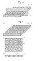
- the plane shape of the modified refractive index areas unevenly changes along the vertical direction. That is, as shown in Fig. 2, the section 24 of the modified refractive index area 23 on a plane 22 sectioning the body 21 parallel to the plane direction changes its shape if the plane 22 is shifted along the vertical direction.
- Figs. 3(a) to 3(f) show examples of the shape change.
- the boundary line 26 of the modified refractive index area on a section taken at a plane 25 (Fig. 4) perpendicular to the body 21 is convex on the side facing the vertical center line 27 of the modified refractive index area 23. It is concave in (b), crank-shaped in (c) and linearly inclined in (d). Both upper and lower sides of the modified refractive index areas may be closed as in Fig. 3(e). Only one of the upper and lower sides of the modified refractive index areas may be closed, as in Fig. 3(f).
- the periodic arrangement of the large number of the modified refractive index areas provided in the body is designed so that the arrangement of the lattice points at which the refractive index areas are located is expressed as "6mm” in Hermann-Mauguin notation or "C6v” in Schoenflies notation.
- a number of modified refractive index areas whose sectional shape in the plane direction is 3m-symmetrical are located at the lattice points arranged in a 6mm-symmetrical pattern.
- a PBG is created for both the TE-polarized light and the TM-polarized light.
- the non-uniform cross-sectional shape in the vertical direction makes the PBG for the TM-polarized light larger than in the case where the plane shape is uniform in the vertical direction.
- the expansion of the PBG for the TM-polarized light creates a section overlapping the PBG for the TE-polarized light or broadens an existing overlapping section.
- the complete PBG thereby obtained is larger than conventional ones. As a result, there is a higher degree of freedom for designing optical devices using two-dimensional photonic crystals.
- a cladding member i.e. a member whose refractive index differs from that of the body
- Presence of the cladding member on the upper and lower sides of the body flattens the electromagnetic field distribution in the direction perpendicular to the body, thereby increasing the difference between the dielectric band and the air band over the entire distribution of the electromagnetic field.
- the dielectric band and air band ultimately become the origin of a PBG.
- the refractive index of the material of the cladding member may be larger or smaller than that of the body.
- the body of the two-dimensional photonic crystal is made of a material whose refractive index is large enough to create a considerable difference in refractive index between the body and the air. Therefore, it is natural to make the cladding member of a material whose refractive index is smaller than that of the body. If the body is made of Si, it is preferable to use SiO 2 as the material of the cladding member. This material selection allows the use of a commercial SOI (Silicon On Insulator) substrate, which consists of an Si layer laminated onto an SiO 2 layer.
- SOI Silicon On Insulator
- the two-dimensional photonic crystal according to the present invention functions as an optical waveguide device if it is provided with a linear defect of the modified refractive index areas or as an optical resonator device if it is provided with a point-like defect.
- Providing the optical resonator in the vicinity of the optical waveguide makes the crystal function as an optical multiplexer/demultiplexer.
- an energy level (called the "defect level") at which light is allowed to exist within the complete PBG is created only at the linear or point-like defect.
- a ray of light whose wavelength (or frequency) corresponds to the defect level can be present within the defect.
- the complete PBG will not be created if the sectional shape of the modified refractive index areas on a plane parallel to the body is not 3m-symmetrical while it unevenly changes along the vertical direction.
- the two-dimensional photonic crystal will be advantageous in that: (i) it will have a wide TE-PBG, (ii) the waveguide will have a wide transmission wavelength band, and (iii) the optical resonator will have a large Q-value.
- Fig. 5(a) is a perspective view of the body
- Fig. 5(b) is a sectional view of the crystal on a plane parallel to the body
- Fig. 5(c) is a sectional view of the crystal on a plane vertical to the body.
- the slab-shaped body 31 made of Si or other material is provided with holes 32 arranged with a period of a.
- the holes 32 are arranged in a triangular lattice pattern, where the triangular lattice points are arranged in a 6mm-symmetrical pattern.
- the holes 32 are not observable on the surface of the body because the upper and lower sides of the holes 32 are closed (Fig. 5(c)).
- the plane shape of each hole 32 is an equilateral triangle, as shown in Fig. 5(b); this shape satisfies the condition of 3m-symmetry.
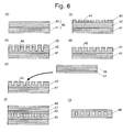
- a method for manufacturing a two-dimensional photonic crystal as shown in Figs. 5(a) to 5(c) is described.
- the method according to the present embodiment uses an SOI substrate 40 consisting of an SiO 2 substrate 41 covered with an Si thin film 42 (Step (a)).
- This film 42 is to be the crystal body.
- a resist 43 is applied onto the Si thin film 42, and then holes 44 whose plane shape is an equilateral triangle are formed in the resist 43 in a triangular lattice pattern (Step (b)). It should be noted that the triangular shape is not shown in Fig. 6 because Fig. 6 shows the vertical section of the Si thin film 42.
- the holes 44 can be created by photolithography, electron beam lithography or other techniques commonly used for manufacturing semiconductor devices.
- the holes 45 shaped like a triangular column are created in the Si thin film 42 by an appropriate method, such as a dry etching process using an etching gas (e.g. SF 6 gas) (Step (c)).
- etching gas e.g. SF 6 gas
- the period of time for the etching process is controlled so that the boring of the holes 45 is discontinued in the middle of the process to leave a portion of the Si thin film 42 on the side of the hole 44 closer to the substrate 41.
- the resist is removed (Step (d)), and the Si thin film 42 is laid onto another Si thin film 47 (Step (e)), which has been separately created beforehand on a substrate 46 made of SiO 2 .
- the two films are adhered to each other (Step (f)).
- the adhering process may be a process of fusing the films at a high temperature from 900 to 1100 degrees Celsius.
- the two Si thin films 42 and 47 are integrated as one.
- the SiO 2 substrates 41 and 46 are removed by an appropriate process, such as a wet etching process using an etchant (e.g. aqueous HF solution) (Step (g)).
- an etchant e.g. aqueous HF solution
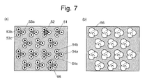
- Figs. 7(a) and 7(b) each show a section of the body on a plane parallel to the body, in which the sectional shape of the holes on the parallel plane is not an equilateral triangle.
- the sectional shape of the holes on a plane perpendicular to the body is the same as shown in Fig. 5(c).
- the example of Fig. 7(a) has three holes 54a, 54b and 54c, each being shaped like a circular column, with their centers located at the apexes 53a, 53b and 53c of the equilateral triangle 52, respectively.
- These three holes integrally function as one modified refractive index area 55.
- This modified refractive index area consisting of the three holes is 3m-symmetrical.
- Such modified refractive index areas 55 are arranged in a triangular lattice pattern.
- the lattice points at which these modified refractive index areas are located are arranged in a 6mm-symmetrical pattern.
- the example in Fig. 7(a) may be modified as in Fig. 7(b), where the three column-like holes 54a, 54b and 54c overlap each other to form a single hole 56.
- the holes 56 are arranged in a triangular lattice pattern.
- the hole 56 is 3m-symmetrical and the lattice points at which the holes 56 are located are arranged in a 6mm-symmetrical pattern.
- the width value of the complete PBG (called the “complete PBG value” hereinafter) has been calculated for some of the above-described two-dimensional photonic crystals according to the present embodiment.
- the results are explained in the following sections.
- the calculation used a three-dimensional finite difference time domain (FDTD) method. Compared with the plane wave expansion method used in Non-Patent Document 1, the three-dimensional FDTD method is more complex and produces more accurate values.
- the results also show the values of the PBG for TM-polarized light (called the "TM-PBG” hereinafter) and the PBG for TE-polarized light (called the "TE-PBG” hereinafter).
- each PBG value is expressed in a percentage value showing the ratio of the PBG width ⁇ to the central value ⁇ 0 of the PBG in terms of frequency.
- the TM-PBG values and the complete PBG values of some conventional two-dimensional photonic crystals were calculated (Fig. 8).
- the body 81 is made of Si.
- the plane shape of the holes 82 is either (i) an equilateral triangle or (ii) a set of three circles with their centers located at the three apexes of a triangular triangle, respectively.
- the filling factor f air i.e. the total volume of the holes divided by that of the body, is 0.45 in (i) and 0.58 in (ii).
- the thickness of the body 81 was 0.8 times as large as the period a of the holes 82.
- the body 81 was in contact with air both the upper and lower sides.
- the body 81 was in contact with air on the upper side and with a cladding member 83 made of SiO 2 on the lower side; the cladding member 83 was much thicker than the body.
- the body 81 was in contact with the cladding members 83 on both the upper and lower sides.
- the complete PBG value of an example of the two-dimensional photonic crystal according to the present invention was calculated (Fig. 9).
- the two-dimensional photonic crystal had holes 82 whose plane shape was an equilateral triangle and which were closed on both upper and lower sides.
- the height of the holes was 0.6 a ; the height of the covers on the upper and lower sides of the holes 82 was 0.1 a on both sides.
- each of the upper and lower sides of the body 81 was in contact with either air or a cladding member 83 made of SiO 2 in a manner as seen in the constructions (a) to (c) of Fig. 8, respectively.
- the TM-PBG value was 2.1 % in (a), 2.6 % in (b) and 3.1 % in (c).
- the TM-PBG is closed in the constructions (b) and (c), whereas the TM-PBG is open in the corresponding constructions of the present example. Therefore, the complete PBG is open only in the present calculation example.
- the present TM-PBG value is larger than that in the comparative example of Fig. 8, so that the complete PBG is accordingly larger.
- the present calculation example has also proved that the provision of the cladding member 83 widens the complete PBG.
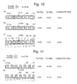
- the complete PBG value of a two-dimensional photonic crystal constructed as shown in Fig. 7(a) was calculated (Fig. 10).
- the plane shape of the holes 82 consisted of three circles whose centers were located at the three apexes of an equilateral rectangle, respectively, and whose upper and lower sides were closed.
- the holes and the cover were 0.6 a and 0.1 a (on both upper and lower sides) in height, respectively.
- the holes and the cover were 0.7 a and 0.05 a in height, respectively.
- the cladding members 83 made of SiO 2 were provided on both upper and lower sides of the construction (b).
- the completed PBG value was 2.0 % in (a), 3.5 % in (b) and 3.2 % in (c). Any of these values is larger than those in the comparative examples.
- This result shows that, if the thickness of the body is the same (0.8 a in the present case), the complete PBG value changes if the height of the holes is changed.
- the complete PBG is smaller than the TM-PBG. This is because only a portion of the TM-PBG overlaps the TE-PBG in the cases of Figs. 10(a) and 10(c), whereas the TM-PBG is entirely included in the energy range of the TE-PBG in the cases of the first calculation example and Fig. 10(b).
- the complete PBG of another two-dimensional photonic crystal was calculated (Fig. 11), in which the plane shape of the holes 82 was as shown in Fig. 7(b) and only the lower side of the holes was closed.
- the height of the holes was 0.75 a
- the height of the cover provided only on the lower side of the holes was 0.05 a
- the cladding member 83 made of SiO 2 was provided only on the lower side. The calculation showed that the complete PBG value was 4.4 % in (a) and 3.0 % in (b).
- the complete PBG obtained in (a) was larger than any other example.
Landscapes
- Engineering & Computer Science (AREA)
- Physics & Mathematics (AREA)
- Optics & Photonics (AREA)
- Chemical & Material Sciences (AREA)
- Nanotechnology (AREA)
- Microelectronics & Electronic Packaging (AREA)
- General Physics & Mathematics (AREA)
- Life Sciences & Earth Sciences (AREA)
- Biophysics (AREA)
- Crystallography & Structural Chemistry (AREA)
- Optical Integrated Circuits (AREA)
Applications Claiming Priority (2)
| Application Number | Priority Date | Filing Date | Title |
|---|---|---|---|
| JP2004249582A JP4297358B2 (ja) | 2004-08-30 | 2004-08-30 | 2次元フォトニック結晶及びそれを用いた光デバイス |
| PCT/JP2005/015691 WO2006025343A1 (ja) | 2004-08-30 | 2005-08-30 | 2次元フォトニック結晶及びそれを用いた光デバイス |
Publications (1)
| Publication Number | Publication Date |
|---|---|
| EP1791007A1 true EP1791007A1 (de) | 2007-05-30 |
Family
ID=35999995
Family Applications (1)
| Application Number | Title | Priority Date | Filing Date |
|---|---|---|---|
| EP05781417A Withdrawn EP1791007A1 (de) | 2004-08-30 | 2005-08-30 | Zweidimensionaler photonischer kristall und optische einrichtung damit |
Country Status (5)
| Country | Link |
|---|---|
| US (1) | US7711228B2 (de) |
| EP (1) | EP1791007A1 (de) |
| JP (1) | JP4297358B2 (de) |
| CN (1) | CN101019052A (de) |
| WO (1) | WO2006025343A1 (de) |
Families Citing this family (33)
| Publication number | Priority date | Publication date | Assignee | Title |
|---|---|---|---|---|
| JP5037835B2 (ja) * | 2006-02-28 | 2012-10-03 | キヤノン株式会社 | 垂直共振器型面発光レーザ |
| JP4900572B2 (ja) | 2006-03-20 | 2012-03-21 | 国立大学法人京都大学 | 2次元フォトニック結晶 |
| JP5352787B2 (ja) * | 2006-08-28 | 2013-11-27 | 国立大学法人京都大学 | 2次元フォトニック結晶熱輻射光源 |
| JP5413369B2 (ja) | 2008-10-09 | 2014-02-12 | 日産化学工業株式会社 | 電荷輸送性ワニス |
| US11726332B2 (en) | 2009-04-27 | 2023-08-15 | Digilens Inc. | Diffractive projection apparatus |
| IT1396797B1 (it) | 2009-12-09 | 2012-12-14 | Sesia | Dispositivo lavaruote |
| WO2016020630A2 (en) | 2014-08-08 | 2016-02-11 | Milan Momcilo Popovich | Waveguide laser illuminator incorporating a despeckler |
| CN102612188B (zh) * | 2012-03-21 | 2014-07-30 | 天津理工大学 | 嵌入自组装空气孔光子晶体薄膜的发光器件及其制备方法 |
| EP2842003B1 (de) | 2012-04-25 | 2019-02-27 | Rockwell Collins, Inc. | Holographisches weitwinkeldisplay |
| US9933684B2 (en) | 2012-11-16 | 2018-04-03 | Rockwell Collins, Inc. | Transparent waveguide display providing upper and lower fields of view having a specific light output aperture configuration |
| WO2014158422A1 (en) * | 2013-03-13 | 2014-10-02 | The Board Of Trustees Of The Leland Stanford Junior University | Confocal and concave 1d photonic crystal resonant cavities with ultra-low mode volume |
| WO2016042283A1 (en) | 2014-09-19 | 2016-03-24 | Milan Momcilo Popovich | Method and apparatus for generating input images for holographic waveguide displays |
| US10437064B2 (en) | 2015-01-12 | 2019-10-08 | Digilens Inc. | Environmentally isolated waveguide display |
| US9632226B2 (en) | 2015-02-12 | 2017-04-25 | Digilens Inc. | Waveguide grating device |
| WO2017038961A1 (ja) * | 2015-09-03 | 2017-03-09 | 丸文株式会社 | 深紫外led及びその製造方法 |
| WO2017060665A1 (en) | 2015-10-05 | 2017-04-13 | Milan Momcilo Popovich | Waveguide display |
| EP3548939A4 (de) | 2016-12-02 | 2020-11-25 | DigiLens Inc. | Wellenleitervorrichtung mit gleichmässiger ausgabebeleuchtung |
| US10545346B2 (en) | 2017-01-05 | 2020-01-28 | Digilens Inc. | Wearable heads up displays |
| GB201705160D0 (en) | 2017-03-30 | 2017-05-17 | Wave Optics Ltd | Waveguide for an augmented reality or virtual reality display |
| JP7456929B2 (ja) | 2018-01-08 | 2024-03-27 | ディジレンズ インコーポレイテッド | 導波管セルを製造するためのシステムおよび方法 |
| JP7404243B2 (ja) | 2018-01-08 | 2023-12-25 | ディジレンズ インコーポレイテッド | 導波管セル内のホログラフィック格子の高スループット記録のためのシステムおよび方法 |
| CN114721242B (zh) | 2018-01-08 | 2025-08-15 | 迪吉伦斯公司 | 用于制造光学波导的方法 |
| WO2020149956A1 (en) | 2019-01-14 | 2020-07-23 | Digilens Inc. | Holographic waveguide display with light control layer |
| US20200247017A1 (en) | 2019-02-05 | 2020-08-06 | Digilens Inc. | Methods for Compensating for Optical Surface Nonuniformity |
| US20220283377A1 (en) | 2019-02-15 | 2022-09-08 | Digilens Inc. | Wide Angle Waveguide Display |
| EP3924759B1 (de) | 2019-02-15 | 2025-07-30 | Digilens Inc. | Verfahren und vorrichtungen zur herstellung einer holografischen wellenleiteranzeige mit integrierten gittern |
| EP3980825A4 (de) | 2019-06-07 | 2023-05-03 | Digilens Inc. | Wellenleiter mit durchlässigen und reflektierenden gittern sowie zugehörige herstellungsverfahren |
| JP2022546413A (ja) | 2019-08-29 | 2022-11-04 | ディジレンズ インコーポレイテッド | 真空回折格子および製造方法 |
| WO2022150841A1 (en) | 2021-01-07 | 2022-07-14 | Digilens Inc. | Grating structures for color waveguides |
| KR20230153459A (ko) | 2021-03-05 | 2023-11-06 | 디지렌즈 인코포레이티드. | 진공 주기적 구조체 및 제조 방법 |
| CN113419303B (zh) * | 2021-06-11 | 2022-06-14 | 太原理工大学 | 一种二维六方氮化硼能谷光子晶体单向光传输结构 |
| CN115308163B (zh) * | 2022-07-06 | 2024-10-29 | 湖北科技学院 | 一种基于缺陷光子晶体中合成角度gh位移的病理切片检测结构及检测方法 |
| JPWO2024176971A1 (de) * | 2023-02-24 | 2024-08-29 |
Family Cites Families (15)
| Publication number | Priority date | Publication date | Assignee | Title |
|---|---|---|---|---|
| US5406573A (en) * | 1992-12-22 | 1995-04-11 | Iowa State University Research Foundation | Periodic dielectric structure for production of photonic band gap and method for fabricating the same |
| DE19526734A1 (de) * | 1995-07-21 | 1997-01-23 | Siemens Ag | Optische Struktur und Verfahren zu deren Herstellung |
| JP3472180B2 (ja) * | 1999-03-08 | 2003-12-02 | 日本電信電話株式会社 | 3次元周期構造体及び2次元周期構造体並びにそれらの作製方法 |
| JP3925769B2 (ja) | 2000-03-24 | 2007-06-06 | 関西ティー・エル・オー株式会社 | 2次元フォトニック結晶及び合分波器 |
| JP4672839B2 (ja) | 2000-09-06 | 2011-04-20 | キヤノン株式会社 | 発光体、構造体及びその製造方法 |
| JP4702870B2 (ja) * | 2001-07-27 | 2011-06-15 | 独立行政法人理化学研究所 | 3次元フォトニック結晶およびその製造方法ならびにプローブ |
| US6728457B2 (en) | 2002-07-10 | 2004-04-27 | Agilent Technologies, Inc. | Waveguides in two dimensional slab photonic crystals with noncircular holes |
| CN1692291A (zh) * | 2002-08-01 | 2005-11-02 | 纳诺普托公司 | 精密相位延迟装置和其制造方法 |
| JP2004125919A (ja) * | 2002-09-30 | 2004-04-22 | Mitsui Chemicals Inc | 偏光分離素子 |
| US7349612B2 (en) * | 2003-01-28 | 2008-03-25 | Nippon Sheet Glass Company, Limited | Optical element, optical circuit provided with the optical element, and method for producing the optical element |
| JP3999152B2 (ja) | 2003-03-25 | 2007-10-31 | アルプス電気株式会社 | 2次元フォトニック結晶スラブ及びこれを用いた光デバイス |
| JP4735259B2 (ja) * | 2003-06-19 | 2011-07-27 | 日本電気株式会社 | フォトニック結晶の構造 |
| US7682551B2 (en) * | 2003-07-01 | 2010-03-23 | Murata Manufacturing Co., Ltd. | Method for manufacturing three-dimensional photonic structure |
| JP4538718B2 (ja) * | 2003-08-28 | 2010-09-08 | アルプス電気株式会社 | 2次元フォトニック結晶スラブ及び2次元フォトニック結晶導波路 |
| JP2005157336A (ja) * | 2003-11-07 | 2005-06-16 | Canon Inc | 光素子の作製方法、3次元積層構造を有する光素子 |
-
2004
- 2004-08-30 JP JP2004249582A patent/JP4297358B2/ja not_active Expired - Fee Related
-
2005
- 2005-08-30 CN CNA2005800284727A patent/CN101019052A/zh active Pending
- 2005-08-30 WO PCT/JP2005/015691 patent/WO2006025343A1/ja not_active Ceased
- 2005-08-30 EP EP05781417A patent/EP1791007A1/de not_active Withdrawn
- 2005-08-30 US US11/661,232 patent/US7711228B2/en not_active Expired - Fee Related
Non-Patent Citations (1)
| Title |
|---|
| See references of WO2006025343A1 * |
Also Published As
| Publication number | Publication date |
|---|---|
| JP4297358B2 (ja) | 2009-07-15 |
| US20080013902A1 (en) | 2008-01-17 |
| JP2006065150A (ja) | 2006-03-09 |
| US7711228B2 (en) | 2010-05-04 |
| WO2006025343A1 (ja) | 2006-03-09 |
| CN101019052A (zh) | 2007-08-15 |
Similar Documents
| Publication | Publication Date | Title |
|---|---|---|
| US7711228B2 (en) | Two-dimensional photonic crystal and optical device using the crystal | |
| JP4923234B2 (ja) | 2次元フォトニック結晶及びそれを用いた光デバイス | |
| US7509014B2 (en) | Two-dimensional photonic crystal having air-bridge structure and method for manufacturing such a crystal | |
| US7321707B2 (en) | Electromagnetic wave frequency filter | |
| EP1560048B1 (de) | Optischer Isolator mit einem Mikroresonator | |
| US7853111B2 (en) | Two-dimensional photonic crystal | |
| JP5272173B2 (ja) | 2次元フォトニック結晶 | |
| JP2003279764A (ja) | 2次元フォトニック結晶光分合波器 | |
| WO2007108219A1 (ja) | 2次元フォトニック結晶 | |
| US20040086244A1 (en) | Optical waveguide structure | |
| JP4063740B2 (ja) | エアブリッジ構造を有する2次元フォトニック結晶及びその製造方法 | |
| US20080112679A1 (en) | Two-Dimensional Photonic Crystal | |
| JP3886958B2 (ja) | 細線導波路付2次元フォトニック結晶の製造方法 | |
| JP2004045924A (ja) | 幾何学的に配列した格子欠陥を有する2次元フォトニック結晶 | |
| JP3920260B2 (ja) | 細線導波路付2次元フォトニック結晶の製造方法 | |
| US6993234B1 (en) | Photonic crystal resonator apparatus with improved out of plane coupling | |
| JP2004295043A (ja) | 光導波路 | |
| US20040146242A1 (en) | Method and structure for coupling light in and out of an inplane waveguide through the top and bottom surfaces of photonic crystals | |
| JP2007523358A (ja) | 光導波路を備えた光デバイス及びその製造方法 |
Legal Events
| Date | Code | Title | Description |
|---|---|---|---|
| PUAI | Public reference made under article 153(3) epc to a published international application that has entered the european phase |
Free format text: ORIGINAL CODE: 0009012 |
|
| 17P | Request for examination filed |
Effective date: 20070323 |
|
| AK | Designated contracting states |
Kind code of ref document: A1 Designated state(s): DE FR GB |
|
| RBV | Designated contracting states (corrected) |
Designated state(s): DE FR GB |
|
| DAX | Request for extension of the european patent (deleted) | ||
| RBV | Designated contracting states (corrected) |
Designated state(s): DE FR GB |
|
| STAA | Information on the status of an ep patent application or granted ep patent |
Free format text: STATUS: THE APPLICATION HAS BEEN WITHDRAWN |
|
| 18W | Application withdrawn |
Effective date: 20080828 |