EP1780779A2 - Verfahren zum Plasma-Ätzen von Gatterstappelung - Google Patents
Verfahren zum Plasma-Ätzen von Gatterstappelung Download PDFInfo
- Publication number
- EP1780779A2 EP1780779A2 EP06121143A EP06121143A EP1780779A2 EP 1780779 A2 EP1780779 A2 EP 1780779A2 EP 06121143 A EP06121143 A EP 06121143A EP 06121143 A EP06121143 A EP 06121143A EP 1780779 A2 EP1780779 A2 EP 1780779A2
- Authority
- EP
- European Patent Office
- Prior art keywords
- plasma
- composition
- stack
- nitrogen
- boron
- Prior art date
- Legal status (The legal status is an assumption and is not a legal conclusion. Google has not performed a legal analysis and makes no representation as to the accuracy of the status listed.)
- Ceased
Links
Images




Classifications
-
- H—ELECTRICITY
- H10—SEMICONDUCTOR DEVICES; ELECTRIC SOLID-STATE DEVICES NOT OTHERWISE PROVIDED FOR
- H10P—GENERIC PROCESSES OR APPARATUS FOR THE MANUFACTURE OR TREATMENT OF DEVICES COVERED BY CLASS H10
- H10P50/00—Etching of wafers, substrates or parts of devices
- H10P50/20—Dry etching; Plasma etching; Reactive-ion etching
- H10P50/26—Dry etching; Plasma etching; Reactive-ion etching of conductive or resistive materials
- H10P50/264—Dry etching; Plasma etching; Reactive-ion etching of conductive or resistive materials by chemical means
- H10P50/266—Dry etching; Plasma etching; Reactive-ion etching of conductive or resistive materials by chemical means by vapour etching only
- H10P50/267—Dry etching; Plasma etching; Reactive-ion etching of conductive or resistive materials by chemical means by vapour etching only using plasmas
-
- H—ELECTRICITY
- H10—SEMICONDUCTOR DEVICES; ELECTRIC SOLID-STATE DEVICES NOT OTHERWISE PROVIDED FOR
- H10D—INORGANIC ELECTRIC SEMICONDUCTOR DEVICES
- H10D64/00—Electrodes of devices having potential barriers
- H10D64/01—Manufacture or treatment
- H10D64/013—Manufacture or treatment of electrodes having a conductor capacitively coupled to a semiconductor by an insulator
- H10D64/01302—Manufacture or treatment of electrodes having a conductor capacitively coupled to a semiconductor by an insulator the insulator being formed after the semiconductor body, the semiconductor being silicon
- H10D64/01304—Manufacture or treatment of electrodes having a conductor capacitively coupled to a semiconductor by an insulator the insulator being formed after the semiconductor body, the semiconductor being silicon characterised by the conductor
- H10D64/01314—Manufacture or treatment of electrodes having a conductor capacitively coupled to a semiconductor by an insulator the insulator being formed after the semiconductor body, the semiconductor being silicon characterised by the conductor the conductor comprising a layer of Ge, C or of compounds of Si, Ge or C contacting the insulator
-
- H—ELECTRICITY
- H10—SEMICONDUCTOR DEVICES; ELECTRIC SOLID-STATE DEVICES NOT OTHERWISE PROVIDED FOR
- H10D—INORGANIC ELECTRIC SEMICONDUCTOR DEVICES
- H10D64/00—Electrodes of devices having potential barriers
- H10D64/01—Manufacture or treatment
- H10D64/013—Manufacture or treatment of electrodes having a conductor capacitively coupled to a semiconductor by an insulator
- H10D64/01302—Manufacture or treatment of electrodes having a conductor capacitively coupled to a semiconductor by an insulator the insulator being formed after the semiconductor body, the semiconductor being silicon
- H10D64/01304—Manufacture or treatment of electrodes having a conductor capacitively coupled to a semiconductor by an insulator the insulator being formed after the semiconductor body, the semiconductor being silicon characterised by the conductor
- H10D64/01318—Manufacture or treatment of electrodes having a conductor capacitively coupled to a semiconductor by an insulator the insulator being formed after the semiconductor body, the semiconductor being silicon characterised by the conductor the conductor comprising a layer of alloy material, compound material or organic material contacting the insulator, e.g. TiN
-
- H—ELECTRICITY
- H10—SEMICONDUCTOR DEVICES; ELECTRIC SOLID-STATE DEVICES NOT OTHERWISE PROVIDED FOR
- H10D—INORGANIC ELECTRIC SEMICONDUCTOR DEVICES
- H10D64/00—Electrodes of devices having potential barriers
- H10D64/60—Electrodes characterised by their materials
- H10D64/66—Electrodes having a conductor capacitively coupled to a semiconductor by an insulator, e.g. MIS electrodes
- H10D64/68—Electrodes having a conductor capacitively coupled to a semiconductor by an insulator, e.g. MIS electrodes characterised by the insulator, e.g. by the gate insulator
- H10D64/681—Electrodes having a conductor capacitively coupled to a semiconductor by an insulator, e.g. MIS electrodes characterised by the insulator, e.g. by the gate insulator having a compositional variation, e.g. multilayered
- H10D64/685—Electrodes having a conductor capacitively coupled to a semiconductor by an insulator, e.g. MIS electrodes characterised by the insulator, e.g. by the gate insulator having a compositional variation, e.g. multilayered being perpendicular to the channel plane
-
- H—ELECTRICITY
- H10—SEMICONDUCTOR DEVICES; ELECTRIC SOLID-STATE DEVICES NOT OTHERWISE PROVIDED FOR
- H10D—INORGANIC ELECTRIC SEMICONDUCTOR DEVICES
- H10D64/00—Electrodes of devices having potential barriers
- H10D64/60—Electrodes characterised by their materials
- H10D64/66—Electrodes having a conductor capacitively coupled to a semiconductor by an insulator, e.g. MIS electrodes
- H10D64/68—Electrodes having a conductor capacitively coupled to a semiconductor by an insulator, e.g. MIS electrodes characterised by the insulator, e.g. by the gate insulator
- H10D64/691—Electrodes having a conductor capacitively coupled to a semiconductor by an insulator, e.g. MIS electrodes characterised by the insulator, e.g. by the gate insulator comprising metallic compounds, e.g. metal oxides or metal silicates
-
- H—ELECTRICITY
- H10—SEMICONDUCTOR DEVICES; ELECTRIC SOLID-STATE DEVICES NOT OTHERWISE PROVIDED FOR
- H10P—GENERIC PROCESSES OR APPARATUS FOR THE MANUFACTURE OR TREATMENT OF DEVICES COVERED BY CLASS H10
- H10P50/00—Etching of wafers, substrates or parts of devices
- H10P50/20—Dry etching; Plasma etching; Reactive-ion etching
- H10P50/28—Dry etching; Plasma etching; Reactive-ion etching of insulating materials
- H10P50/282—Dry etching; Plasma etching; Reactive-ion etching of insulating materials of inorganic materials
- H10P50/283—Dry etching; Plasma etching; Reactive-ion etching of insulating materials of inorganic materials by chemical means
- H10P50/285—Dry etching; Plasma etching; Reactive-ion etching of insulating materials of inorganic materials by chemical means of materials not containing Si, e.g. PZT or Al2O3
-
- H—ELECTRICITY
- H10—SEMICONDUCTOR DEVICES; ELECTRIC SOLID-STATE DEVICES NOT OTHERWISE PROVIDED FOR
- H10D—INORGANIC ELECTRIC SEMICONDUCTOR DEVICES
- H10D30/00—Field-effect transistors [FET]
- H10D30/60—Insulated-gate field-effect transistors [IGFET]
Definitions
- the present invention is related to the field of semiconductor processing. More specifically it is related to the dry etching of advanced gate stacks, in particular to metal gate comprising stacks and pure germanium comprising stacks.
- the invention is further related to an etch plasma composition and its use for dry etching of metal gate comprising stacks and pure germanium comprising stacks thereby preserving the vertical profile of the gate stack after patterning.
- Etching of metal gates has been studied addressing metal gate and gate oxide surface roughness, CD control, etch selectivity, and low damage etching but none of them succeeded in preserving the vertical profile of the gate stack after patterning.
- BCl 3 One of the promising chemistry for patterning of advanced gate stacks (metal gate etch or high-k removal) is BCl 3 .
- the main advantage of this plasma is that it can etch both metal gates and high-k dielectric with reasonable selectivity to the Si substrate.
- Two particular examples are Ge gates and TaN metal gates. If a pure BCl 3 plasma is applied during the patterning of the gate stacks containing Ge or TaN a profile distortion caused by lateral etch is observed.
- the present invention discloses a dry-etch plasma composition for preserving the vertical profile of a structure comprising a stack of layers during anisotropical dry-etch patterning.
- Said plasma composition is further characterized such that during the dry-etch patterning of said stack a water-soluble film, which is removable against the structure, is deposited onto the sidewalls of said stack such that lateral attack of said patterned stack is avoided.
- the plasma composition of the present invention is characterized as a plasma comprising a boron-halogen compound and nitrogen and wherein the ratio of the boron-halogen compound to nitrogen is from 19:1 up to 9:1. More preferred, the plasma composition of the present invention is characterized as a plasma composition wherein said plasma comprises a boron-halogen compound, nitrogen and optionally an inert compound. Most preferred said boron-halogen compound is BCl 3 .
- the plasma composition of the present invention is characterized as a plasma comprising (or consisting of) a boron-halogen compound and 5 up to 10% nitrogen (of the total plasma composition).
- the plasma composition comprises (or consists of) a boron-halogen compound and less than 10% nitrogen (of the total plasma composition). More particularly, said boron-halogen compound is BCl 3 .
- said plasma is (i.e. consists of) a BCl 3 plasma further comprising (or to which is added) from 5% to 10% nitrogen (based on the total plasma composition).
- the stack of layers to be patterned is a metal gate comprising stack.
- said metal gate comprising stack comprises at least one TaN layer or combinations of a TaN layer and a TiN layer (referred to as TaN/TiN metal gates) wherein said TaN layer is too sensitive to a (pure) BCl 3 plasma.
- the stack of layers to be patterned is a stack wherein at least one layer of said stack of layers is a TaN layer.
- At least one layer of said stack of layers to be patterned is a germanium comprising layer.
- Said germanium layer can be situated upon a layer to be patterned by the plasma composition of the present invention.
- Said germanium layer can be a pure Ge layer.
- the plasma of the present invention (during patterning) has a substrate bias which is different from zero.
- the plasma of the present invention has a plasma power is in the range of 100W up to 1200W. More preferred said plasma power is around 450W.
- the plasma of the present invention has a pressure in the plasma chamber of minimum 0.666 Pa (5mT) and maximum 10.665 Pa (80mT). More preferred said pressure is 0.666 Pa (5mT).
- the plasma of the present invention (during patterning) has a temperature below 100°C and most preferred said plasma temperature during dry-etch patterning is around 60°C.
- An anisotropical dry etching method is also disclosed using the plasma composition of the present invention as described above for patterning a stack of layers to create a vertical structure wherein lateral attack during patterning of said stack is avoided.
- said method comprises the steps of first applying a dry-etch step using the plasma composition of the invention wherein during the etching a protective and water-soluble film is deposited onto the vertical sidewalls of said structure such that the vertical profile of said structure is preserved and lateral attack is avoided. In a next step said water-soluble film is removed from said structure.
- Said water-soluble film is preferably removed using a wet removal process using water.
- the present invention also relates to the use of a plasma comprising (or consisting of) BCl 3 , to which nitrogen is added to reach 5% to 10% of the total volume of the resulting plasma composition, for etching a (suitable) stack of layer (i.e. comprising at least one layer etchable by said BCl 3 component) and simultaneously passivating (or protecting) the sidewalls of said stack of layers from lateral etch.
- a plasma comprising (or consisting of) BCl 3 , to which nitrogen is added to reach 5% to 10% of the total volume of the resulting plasma composition, for etching a (suitable) stack of layer (i.e. comprising at least one layer etchable by said BCl 3 component) and simultaneously passivating (or protecting) the sidewalls of said stack of layers from lateral etch.
- the present invention also relates to a method for etching (or patterning) a (suitable) stack of layers while/and simultaneously passivating (or protecting) the sidewalls of said stack of layers comprising the step of providing a plasma comprising (or consisting of) BCl 3 , to which nitrogen is added to reach 5% to 10% of the total volume of the resulting plasma composition.
- Said use or said method is particularly useful for (patterning) a stack of layers wherein at least one layer is germanium, or at least one layer is TaN.
- Said passivating (or protecting) effect results from the formation and deposition of a film (or layer) which contains boron and nitrogen (and further compounds such as oxygen) on the sidewalls of said stack of layers.
- Said film obtainable by a method of the invention is also an object of the present invention.
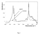
- Figure 1 shows FTIR (Fourier Transform Infrared Spectroscopy) spectra of films deposited from BCl 3 /N 2 plasma mixture (70% BCl 3 ) at 275°C and 60°C.
- Figure 2 shows a Ge gate profile after the gate patterning and before the high-k removal.
- Figure 3 shows a Ge gate profile after high-k removal by pure BCl 3 plasma for 10 seconds (Figure 3A) and BCl 3 /N 2 (10% N 2 ) plasma for 20 seconds ( Figure 3B).
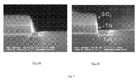
- Figure 4 shows a TaN gate profile after etching in pure BCl 3 plasma ( Figure 4A), an arrow indicates the lateral attack of TaN.
- Figure 4B shows a TaN gate profile after etching in BCl 3 /N 2 (5% N 2 ) plasma.
- Figure 5 shows a TaN gate profile after etching in BCl 3 /N 2 plasma (Figure 5A) and a TaN gate profile after etching in BCl 3 /O 2 plasma ( Figure 5B).
- critical dimension refers to the smallest dimensions of geometrical features (e.g. width of gate electrode) which can be formed during semiconductor device manufacturing.
- bias refers to the voltage applied to the substrate during patterning in a dry etch chamber.
- selectivity refers to the etch rate of a selected material towards another material.
- the material to be etched away should have a much higher etch rate than the other materials.
- ratio is expressed as amount of a first compound to a second compound, e.g. a ratio of 9:1 means e.g. 9 sccm (standard centimeter cube per minute) of the first compound and 1 sccm of the second compound.
- the invention is based on the surprising effect of using a plasma composition according to the invention, i.e. the deposition of a BxNy film during the etching of a structure wherein the deposition is performed in a plasma etch chamber (e.g. Versys 2300 etch chamber from LAM®) at low temperatures (e.g. 60°C), which was never reported before (BN deposition is usually performed at temperatures in the range 390°C-650°C).
- the BxNy film is deposited at a rate as high as e.g. 300 nm/min depending on the pressure, plasma power, gas flows and plasma composition (more specifically the BCl 3 to N 2 ratio). Said deposited BxNy-like film, in contrast to a pure BN film, was found to be easily decomposing by temperature (the film thickness decreases at temperatures above 100°C) and soluble in water at room temperatures.
- the present invention is further related to the patterning of a stack of layers, more specifically to the dry etching of a stack of layers.
- Said patterning is making use of a plasma etch compound wherein at least one of the layers is too sensitive to said etch compound.
- a protective layer onto the stack of layers such that said stack is protected for e.g. sidewall damage.
- Said protective layer is deposited during the patterning (dry etching). Furthermore said protective layer is sacrificial and hence easy removable.
- the "sacrificial" layer also referred to as "protective” layer or “passivation” layer refers to the BxNy like film resulting from the addition of nitrogen in the boron-halogen plasma, also referred to as BxNy film or as to boron nitride like film, which is deposited during etching.
- Said BxNy film is used as a "protective” or “passivating” film during patterning/etching of a structure, said BxNy film is also referred to as a sacrificial layer because said layer is removed after patterning is completed. Due the unstable character of the BxNy film and water soluble character said BxNy film can be easily removed by e.g. a water rinse.
- BxNy film refers to a film comprising mainly boron and nitrogen which is further characterized as a water-soluble film.
- the BxNy film of the invention is water soluble, in contrast to a pure BN which is insoluble in water.
- the BxNy film is therefore referred to as BxNy wherein the integers x and y indicate that the ratio of nitrogen and boron in the film is not fixed due to the presence of other compounds (impurities) in the film such as water, oxygen and/or ammonia which are possibly absorbed from the plasma and/or atmosphere after dry-etching.
- the present invention relates to the patterning of metal gate stacks or germanium gate stacks, more specifically it relates to the dry etching of said gate stacks such as TaN comprising metal gate stacks and to the dry etching of Ge comprising stacks (or in other words a stack comprising e.g. a pure Ge layer).
- the present invention solves the problem of lateral etch and profile attack during the patterning of advanced gate stacks such as metal gate stacks and germanium stacks by adding small amounts of nitrogen to a boron-halogen plasma such as BCl 3 plasma in order to improve gate profile control.
- a boron-halogen plasma such as BCl 3 plasma
- the mixture of BCl 3 /N 2 plasma results in a deposition of BxNy-like film that inhibits the lateral etch but does not inhibit vertical etch as the formed BxNy-like film is destroyed by ion bombardment.
- a plasma composition for patterning metal gate stacks and/or germanium stacks wherein during the patterning of said stack a protective and water-soluble film is deposited such that the vertical profile of the stack is preserved and lateral attack of said stack is avoided.
- a plasma composition for patterning a stack of layers wherein at least one layer of said stack is sensitive to one of the etch compounds.
- the plasma composition is preferably a Boron-halogen comprising plasma with small additions of nitrogen.
- the Boron-halogen compound is preferably BCl 3 and said small additions of nitrogen are such that the ratio of the boron-halogen compound to nitrogen is in the range of 19:1 up to 9:1.
- an inert compound can be added to the plasma comprising boron-halogen and nitrogen.
- Said inert compound can be e.g. argon or helium (He) and these compounds can be added to the plasma in concentrations up to 50% of the total plasma composition.
- the ratio of the boron-halogen compound to nitrogen is below 9:1 (having more boron-halogen), more preferred said ratio of the boron-halogen compound to nitrogen is below 11:1 and most preferred said ratio of the boron-halogen compound to nitrogen is 19:1.
- the ratio of BCl 3 to nitrogen is below 9:1, more preferred said ratio of BCl 3 to nitrogen is below 11:1 and most preferred said ratio of BCl 3 to nitrogen is 19:1.
- the ratio of the boron-halogen compound to nitrogen is higher than 19:1. More preferred said ratio of the boron-halogen compound to nitrogen is higher than 11:1 and most preferred the ratio of the boron-halogen compound to nitrogen is 9:1.
- the ratio of BCl 3 to nitrogen is higher than 19:1. More preferred said ratio of BCl 3 to nitrogen is higher than 11:1 and most preferred the ratio of BCl 3 to nitrogen is 9:1.
- the plasma composition is preferably a plasma comprising (or consisting of) a Boron-halogen compound and nitrogen, or in other words small additions of nitrogen in a boron-halogen plasma.
- the plasma comprises (or consists of) a boron-halogen compound and 5% up to 10% nitrogen (of the total plasma composition).
- the plasma composition comprises (or consists of) a boron-halogen compound and less than 10% nitrogen (of the total plasma composition) and most preferred said boron-halogen is BCl 3 .
- the amount of N 2 to the total BCl 3 /N 2 plasma composition is higher than 5%, more preferred said amount of N 2 is higher than 8% N 2 to the total BCl 3 /N 2 plasma composition and most preferred said amount of N 2 is 10% to the total BCl 3 /N 2 plasma composition.
- the amount of N 2 to the total BCl 3 /N 2 plasma composition is lower than 10%, more preferred said amount of N 2 is lower than 8% N 2 to the total BCl 3 /N 2 plasma composition and most preferred said amount of N 2 is 5% to the total BCl 3 /N 2 plasma composition.
- the plasma of the present invention (during patterning) has a substrate bias which is different from zero.
- the plasma of the present invention has a plasma power is in the range of 100W up to 1200W. More preferred said plasma power is around 450W.
- the plasma of the present invention has a pressure in the plasma chamber of minimum 0.666 Pa (5mT) and maximum 10.665 Pa (80mT). More preferred said pressure is 0.666 Pa (5mT).
- the plasma of the present invention (during patterning) has a temperature below 100°C and most preferred said plasma temperature during dry-etch patterning is around 60°C.
- a boron-nitrogen (B x N y or BN) film deposited at higher temperatures is equal to a higher quality film containing less (or no) impurities which is more difficult or even not possible to remove.
- non-Si comprising gate stacks are preferably metal gate comprising gate stacks such as TaN comprising gate stacks and preferably metal gate stacks comprising a (pure) germanium layer.
- the dry-etching method of the invention uses a plasma composition wherein at least one layer of said stack is too sensitive to one of the etch compounds.
- Said dry etching method is characterized in that the vertical profile of said gate stack is preserved after etching.
- the method of the invention solves the problem of negatively sloped gate profiles after dry etching by depositing a sacrificial layer during the etching.
- Said sacrificial layer serves as a passivating layer during dry etching such that the vertical profile or CD of the gate stack is preserved.
- the dry-etching method of the invention solves the problem of lateral etch and profile attack during the patterning of advanced gate stacks such as metal gate stacks and germanium comprising stacks by adding small amounts of nitrogen to a boron-halogen plasma such as BCl 3 plasma in order to improve gate profile control.
- a boron-halogen plasma such as BCl 3 plasma
- the mixture of BCl 3 /N 2 plasma results in a deposition of BxNy-like film that inhibits the lateral etch but does not inhibit vertical etch as the formed BxNy-like film is destroyed by ion bombardment.
- the method of the invention comprises the steps of first applying a dry-etch step using the plasma composition of the invention whereby during the etching a protective and water-soluble film is deposited onto the vertical sidewalls of said structure such that the vertical profile of said structure is preserved and lateral attack is avoided. In a next step said water-soluble film is removed from said structure.
- Said water-soluble film is preferably removed using a wet removal process, most preferred said wet removal is using water.
- the dry-etching method of the invention uses a Boron-halogen comprising plasma with small additions of nitrogen.
- the Boron-halogen compound is preferably BCl 3 and said small additions of nitrogen are such that the ratio of the boron-halogen compound to nitrogen is in the range of 19:1 up to 9:1.
- an inert compound can be added to the plasma comprising boron-halogen and nitrogen.
- Said inert compound can be e.g. argon or helium (He) and these compounds can be added to the plasma in concentrations up to 50% of the total plasma composition.
- the ratio of the boron-halogen compound to nitrogen is preferably below 9:1. More preferably, said ratio of the boron-halogen compound to nitrogen is below 11:1 and most preferred said ratio of the boron-halogen compound to nitrogen is 19:1.
- said boron-halogen compound is BCl 3 .
- the ratio of the boron-halogen compound to nitrogen is preferably higher than 19:1. More preferred said ratio of the boron-halogen compound to nitrogen is higher than 11:1 and most preferred the ratio of the boron-halogen compound to nitrogen is 9:1.
- said boron-halogen compound is BCl 3 .
- the plasma composition used in a method of the invention is a plasma comprising (or consisting of) a Boron-halogen compound and nitrogen, or in other words small additions of nitrogen in a boron-halogen plasma.
- the plasma comprises (or consists of) a boron-halogen compound and 5% up to 10% nitrogen (of the total plasma composition).
- the plasma composition comprises (or consists of) a boron-halogen compound and less than 10% nitrogen (of the total plasma composition) and most preferred said boron-halogen is BCl 3 .
- the amount of N 2 to the total BCl 3 /N 2 plasma composition is higher than 5%, more preferred said amount of N 2 is higher than 8% N 2 to the total BCl 3 /N 2 plasma composition and most preferred said amount of N 2 is 10% to the total BCl 3 /N 2 plasma composition.
- the amount of N 2 to the total BCl 3 /N 2 plasma composition is lower than 10%, more preferred said amount of N 2 is lower than 8% N 2 to the total BCl 3 /N 2 plasma composition and most preferred said amount of N 2 is 5% to the total BCl 3 /N 2 plasma composition.
- the plasma used in a method of the invention has a substrate bias which is different from zero.
- said plasma has a plasma power in the range of 100W up to 1200W. More preferred said plasma power is around 450W.
- said plasma has a pressure in the plasma chamber of minimum 0.666 Pa (5mT) and maximum 10.665 Pa (80mT). More preferred said pressure is 0.666 Pa (5mT).
- said plasma has a temperature below 100°C and more preferred said plasma temperature during dry-etch patterning is around 60°C.
- boron-nitrogen (B x N y or BN) film deposited at higher temperatures is equal to a higher quality film containing less (or no) impurities, which is more difficult or even not possible to remove.
- non-Si comprising gate stacks are preferably metal gate comprising gate stacks such as TaN comprising gate stacks and preferably pure germanium comprising metal stacks.
- Said dry etching method is characterized in that the vertical profile of said gate stack is preserved after etching.
- the method of the invention solves the problem of negatively sloped gate profiles after dry etching by depositing a sacrificial layer during the etching. Said sacrificial layer serves as a passivating layer during dry etching such that the vertical profile or CD of the gate stack is preserved.
- the present invention discloses a composition of a plasma used to etch materials that are too sensitive to Cl-based plasmas. If those materials are etched with pure Cl-based plasmas such as BCl 3 plasmas, the etch profiles are distorted because these materials are etched in the lateral direction as well. Examples of said materials are metal gate comprising gate stacks such as TaN comprising gate stacks and pure germanium comprising metal stacks.
- the plasma of the invention solves the problem of damage caused by Cl-based plasmas, more specifically this is achieved by adding small amounts of nitrogen to the Cl-based plasma.
- said Cl compound is preferably BCl 3 .
- the amount of nitrogen added to the plasma is preferably between 5% up to 10%.
- the addition of nitrogen to a Cl-based plasma such as BCl 3 preserves the vertical profile through the formation of a passivating B x N y -like layer on the vertical surfaces.
- Said patterning is further characterized as a patterning which avoids lateral etching and preserves the vertical profile.
- Said stacks are preferably metal gate comprising gate stacks such as TaN comprising gate stacks and preferably pure germanium comprising metal stacks.
- said Cl compound is BCl 3 .
- the method of the current invention as well as the plasma and its use can be applied to any material that can be etched by Cl-based plasma but is too chemically reactive and has significant lateral etch component. Said lateral etch can be blocked by a BxNy-like passivation film deposited onto the vertical sidewalls while at the meanwhile the vertical etch is not significantly affected.
- the BCl 3 /N 2 plasma was applied for patterning of two different stacks as described in example 1 and 2: pure Ge gates and TaN metal gates in the TiN/TaN gate stack. In both cases, the lateral attack of the gate material was prevented by addition of small amount of N 2 (5%-10%) to the BCl 3 plasma. Furthermore the plasma settings were optimized and illustrated in example 3.
- the deposited (passivation) BxNy-like layer of the present invention is characterized by FTIR and illustrated in example 4.
- Example 1 Application of BCl 3 /N 2 plasma for TaN gate profile control.
- the BCl 3 /N 2 plasma was used to etch TaN metal gates, in the example presented here said TaN metal gate is present in a TiN/TaN gate stack where 15 nm TaN is in the contact with the gate dielectric and 70 nm TiN covers the TaN or in other words 70nm TiN is situated on top of said 15 nm TaN.
- the most critical step is TaN etching after TiN patterning.
- BCl 3 plasma is used here for the TaN patterning as it is selective to the Si substrate and can be used as high-k removal as well.
- TaN is etched with pure BCl 3 plasma, then a notch (lateral attack) is observed in the TaN layer.
- Figure 4A shows the gate profile after etching in pure BCl 3 , an arrow indicates the lateral attack of TaN.
- a B x N y comprising passivation layer will be deposited onto the vertical sidewalls of the stack during patterning, said B x N y comprising passivation layer will protect the TaN during patterning and avoid lateral attack.
- the B x N y comprising passivation layer could be removed by a wet treatment e.g. a removal in water.
- Example 2 Application of BCl 3 /N 2 plasma for pure Ge gate profile control.
- the BCl 3 /N 2 plasma was used to pattern pure Ge gates having a high-k dielectric underneath (in the presented case the high-k dielectric is HfO 2 ).
- the high-k dielectric must be removed selectively to the underlying Si substrate.
- Figure 3A shows the Ge gate profile after high-k removal by a pure BCl 3 plasma for 10 seconds and Figure 3B shows the Ge gate profile after high-k removal by a BCl 3 /N 2 (10% N 2 ) plasma for 20 seconds. No lateral attack of the Ge profile is seen in Figure 3B.
- Example 3 Plasma parameters used to deposit a BxNy passivation film.
- the plasma parameters used for the deposition of a BxNy passivation film during TaN metal gate patterning as presented in example 1 using the plasma of the current invention can be as follows:
- the plasma parameters used for the deposition of a BxNy passivation film during high-k removal in a Ge gate stacks as presented in example 2 can be as follows:
- Using the plasma composition (BCl 3 /N 2 ) and method of the present invention resulted in the deposition of a BxNy layer.
- Said BxNy film was characterized by Fourier Transmission Infra-Red spectrometry (FTIR) and X-ray Photoelectron Spectroscopy (XPS). It was found that a plasma mixture of BCl 3 and N 2 resulted in the deposition of a BxNy film onto a (flat) wafer surface if no bias was applied to the substrate (to avoid ion bombardment).
- FTIR Fourier Transmission Infra-Red spectrometry
- XPS X-ray Photoelectron Spectroscopy
- Said BxNy film was deposited in an etch chamber (LAM Versys 2300) at 60°C and 275°C at a rate as high as 300 nm/min depending on the pressure, plasma power, gas flows and BCl 3 to N 2 ratio.
- LAM Versys 2300 etch chamber
- the XPS analysis of the surface of the film deposited at 60°C showed primarily boron (about 36%), nitrogen (about 20%) and oxygen (about 36%). Some carbon (about 7%) is attributed to the contamination from the atmosphere. The amount of chlorine did not exceed 1%. As the deposition plasma contains no O 2 , the significant amount of oxygen in the film is a sign of the film oxidation during the atmosphere exposure.
- the deposited BxNy-like film was found to be easily decomposing by temperature (the film thickness decreases at temperatures above 100°C) and soluble in water at room temperatures. These properties make cleaning of any deposited inhibitor layer easy: the water rinse is enough to clean any BxNy-like film that is left after the gate patterning.
Landscapes
- Drying Of Semiconductors (AREA)
- Insulated Gate Type Field-Effect Transistor (AREA)
- Electrodes Of Semiconductors (AREA)
- Internal Circuitry In Semiconductor Integrated Circuit Devices (AREA)
Priority Applications (5)
| Application Number | Priority Date | Filing Date | Title |
|---|---|---|---|
| US11/544,351 US20070099428A1 (en) | 2005-10-28 | 2006-10-05 | Plasma for patterning advanced gate stacks |
| US11/585,564 US7598184B2 (en) | 2005-10-28 | 2006-10-24 | Plasma composition for selective high-k etch |
| JP2006289915A JP2007123890A (ja) | 2005-10-28 | 2006-10-25 | 改良型ゲートスタックのパターン化用プラズマ |
| JP2006292913A JP5328094B2 (ja) | 2005-10-28 | 2006-10-27 | 選択的に高k材をエッチングするためのプラズマ組成 |
| EP06123197A EP1780780A3 (de) | 2005-10-28 | 2006-10-30 | Plasma-Zusammensetzung für die selektive Ätzung von dielektrischen Schichten mit hoher Dielektrizitätskonstante |
Applications Claiming Priority (1)
| Application Number | Priority Date | Filing Date | Title |
|---|---|---|---|
| US73160805P | 2005-10-28 | 2005-10-28 |
Publications (2)
| Publication Number | Publication Date |
|---|---|
| EP1780779A2 true EP1780779A2 (de) | 2007-05-02 |
| EP1780779A3 EP1780779A3 (de) | 2008-06-11 |
Family
ID=37776895
Family Applications (2)
| Application Number | Title | Priority Date | Filing Date |
|---|---|---|---|
| EP06121143A Ceased EP1780779A3 (de) | 2005-10-28 | 2006-09-22 | Verfahren zum Plasma-Ätzen von Gatterstappelung |
| EP06123197A Ceased EP1780780A3 (de) | 2005-10-28 | 2006-10-30 | Plasma-Zusammensetzung für die selektive Ätzung von dielektrischen Schichten mit hoher Dielektrizitätskonstante |
Family Applications After (1)
| Application Number | Title | Priority Date | Filing Date |
|---|---|---|---|
| EP06123197A Ceased EP1780780A3 (de) | 2005-10-28 | 2006-10-30 | Plasma-Zusammensetzung für die selektive Ätzung von dielektrischen Schichten mit hoher Dielektrizitätskonstante |
Country Status (3)
| Country | Link |
|---|---|
| US (2) | US20070099428A1 (de) |
| EP (2) | EP1780779A3 (de) |
| JP (1) | JP5328094B2 (de) |
Families Citing this family (155)
| Publication number | Priority date | Publication date | Assignee | Title |
|---|---|---|---|---|
| US8183161B2 (en) * | 2006-09-12 | 2012-05-22 | Tokyo Electron Limited | Method and system for dry etching a hafnium containing material |
| US7521369B2 (en) * | 2006-10-23 | 2009-04-21 | Interuniversitair Microelektronica Centrum (Imec) | Selective removal of rare earth based high-k materials in a semiconductor device |
| JP4849614B2 (ja) | 2006-11-01 | 2012-01-11 | 東京エレクトロン株式会社 | 基板処理方法及び基板処理システム |
| US8221636B2 (en) * | 2008-05-12 | 2012-07-17 | Headway Technologies, Inc. | Method of manufacturing magnetic head for perpendicular magnetic recording |
| JPWO2010070826A1 (ja) * | 2008-12-17 | 2012-05-24 | パナソニック株式会社 | 貫通電極の形成方法及び半導体装置 |
| KR20110042614A (ko) * | 2009-10-19 | 2011-04-27 | 삼성전자주식회사 | 반도체 소자 및 그 형성방법 |
| US8313661B2 (en) * | 2009-11-09 | 2012-11-20 | Tokyo Electron Limited | Deep trench liner removal process |
| US9324576B2 (en) | 2010-05-27 | 2016-04-26 | Applied Materials, Inc. | Selective etch for silicon films |
| US10283321B2 (en) | 2011-01-18 | 2019-05-07 | Applied Materials, Inc. | Semiconductor processing system and methods using capacitively coupled plasma |
| US8999856B2 (en) | 2011-03-14 | 2015-04-07 | Applied Materials, Inc. | Methods for etch of sin films |
| US9064815B2 (en) | 2011-03-14 | 2015-06-23 | Applied Materials, Inc. | Methods for etch of metal and metal-oxide films |
| US8771536B2 (en) | 2011-08-01 | 2014-07-08 | Applied Materials, Inc. | Dry-etch for silicon-and-carbon-containing films |
| US8927390B2 (en) | 2011-09-26 | 2015-01-06 | Applied Materials, Inc. | Intrench profile |
| US8808563B2 (en) | 2011-10-07 | 2014-08-19 | Applied Materials, Inc. | Selective etch of silicon by way of metastable hydrogen termination |
| US9267739B2 (en) | 2012-07-18 | 2016-02-23 | Applied Materials, Inc. | Pedestal with multi-zone temperature control and multiple purge capabilities |
| US9373517B2 (en) | 2012-08-02 | 2016-06-21 | Applied Materials, Inc. | Semiconductor processing with DC assisted RF power for improved control |
| US9034770B2 (en) | 2012-09-17 | 2015-05-19 | Applied Materials, Inc. | Differential silicon oxide etch |
| US9023734B2 (en) | 2012-09-18 | 2015-05-05 | Applied Materials, Inc. | Radical-component oxide etch |
| US9390937B2 (en) | 2012-09-20 | 2016-07-12 | Applied Materials, Inc. | Silicon-carbon-nitride selective etch |
| US9132436B2 (en) | 2012-09-21 | 2015-09-15 | Applied Materials, Inc. | Chemical control features in wafer process equipment |
| US8969212B2 (en) | 2012-11-20 | 2015-03-03 | Applied Materials, Inc. | Dry-etch selectivity |
| US8980763B2 (en) | 2012-11-30 | 2015-03-17 | Applied Materials, Inc. | Dry-etch for selective tungsten removal |
| US9111877B2 (en) | 2012-12-18 | 2015-08-18 | Applied Materials, Inc. | Non-local plasma oxide etch |
| US8921234B2 (en) | 2012-12-21 | 2014-12-30 | Applied Materials, Inc. | Selective titanium nitride etching |
| US10256079B2 (en) | 2013-02-08 | 2019-04-09 | Applied Materials, Inc. | Semiconductor processing systems having multiple plasma configurations |
| US9362130B2 (en) | 2013-03-01 | 2016-06-07 | Applied Materials, Inc. | Enhanced etching processes using remote plasma sources |
| US9040422B2 (en) * | 2013-03-05 | 2015-05-26 | Applied Materials, Inc. | Selective titanium nitride removal |
| US8801952B1 (en) | 2013-03-07 | 2014-08-12 | Applied Materials, Inc. | Conformal oxide dry etch |
| US10170282B2 (en) | 2013-03-08 | 2019-01-01 | Applied Materials, Inc. | Insulated semiconductor faceplate designs |
| US20140271097A1 (en) | 2013-03-15 | 2014-09-18 | Applied Materials, Inc. | Processing systems and methods for halide scavenging |
| US8895449B1 (en) | 2013-05-16 | 2014-11-25 | Applied Materials, Inc. | Delicate dry clean |
| US9114438B2 (en) | 2013-05-21 | 2015-08-25 | Applied Materials, Inc. | Copper residue chamber clean |
| US9493879B2 (en) | 2013-07-12 | 2016-11-15 | Applied Materials, Inc. | Selective sputtering for pattern transfer |
| US9773648B2 (en) | 2013-08-30 | 2017-09-26 | Applied Materials, Inc. | Dual discharge modes operation for remote plasma |
| US8956980B1 (en) | 2013-09-16 | 2015-02-17 | Applied Materials, Inc. | Selective etch of silicon nitride |
| US8951429B1 (en) | 2013-10-29 | 2015-02-10 | Applied Materials, Inc. | Tungsten oxide processing |
| US9236265B2 (en) | 2013-11-04 | 2016-01-12 | Applied Materials, Inc. | Silicon germanium processing |
| US9576809B2 (en) | 2013-11-04 | 2017-02-21 | Applied Materials, Inc. | Etch suppression with germanium |
| US9520303B2 (en) | 2013-11-12 | 2016-12-13 | Applied Materials, Inc. | Aluminum selective etch |
| US9245762B2 (en) | 2013-12-02 | 2016-01-26 | Applied Materials, Inc. | Procedure for etch rate consistency |
| US9117855B2 (en) | 2013-12-04 | 2015-08-25 | Applied Materials, Inc. | Polarity control for remote plasma |
| US9263278B2 (en) | 2013-12-17 | 2016-02-16 | Applied Materials, Inc. | Dopant etch selectivity control |
| US9287095B2 (en) | 2013-12-17 | 2016-03-15 | Applied Materials, Inc. | Semiconductor system assemblies and methods of operation |
| US9190293B2 (en) | 2013-12-18 | 2015-11-17 | Applied Materials, Inc. | Even tungsten etch for high aspect ratio trenches |
| US9287134B2 (en) | 2014-01-17 | 2016-03-15 | Applied Materials, Inc. | Titanium oxide etch |
| US9396989B2 (en) | 2014-01-27 | 2016-07-19 | Applied Materials, Inc. | Air gaps between copper lines |
| US9293568B2 (en) | 2014-01-27 | 2016-03-22 | Applied Materials, Inc. | Method of fin patterning |
| US9385028B2 (en) | 2014-02-03 | 2016-07-05 | Applied Materials, Inc. | Air gap process |
| US9499898B2 (en) | 2014-03-03 | 2016-11-22 | Applied Materials, Inc. | Layered thin film heater and method of fabrication |
| US9299575B2 (en) | 2014-03-17 | 2016-03-29 | Applied Materials, Inc. | Gas-phase tungsten etch |
| US9299538B2 (en) | 2014-03-20 | 2016-03-29 | Applied Materials, Inc. | Radial waveguide systems and methods for post-match control of microwaves |
| US9299537B2 (en) | 2014-03-20 | 2016-03-29 | Applied Materials, Inc. | Radial waveguide systems and methods for post-match control of microwaves |
| US9136273B1 (en) | 2014-03-21 | 2015-09-15 | Applied Materials, Inc. | Flash gate air gap |
| JP6163446B2 (ja) * | 2014-03-27 | 2017-07-12 | 株式会社東芝 | 半導体装置の製造方法 |
| US9903020B2 (en) | 2014-03-31 | 2018-02-27 | Applied Materials, Inc. | Generation of compact alumina passivation layers on aluminum plasma equipment components |
| US9269590B2 (en) | 2014-04-07 | 2016-02-23 | Applied Materials, Inc. | Spacer formation |
| US9309598B2 (en) | 2014-05-28 | 2016-04-12 | Applied Materials, Inc. | Oxide and metal removal |
| US9847289B2 (en) | 2014-05-30 | 2017-12-19 | Applied Materials, Inc. | Protective via cap for improved interconnect performance |
| US9406523B2 (en) | 2014-06-19 | 2016-08-02 | Applied Materials, Inc. | Highly selective doped oxide removal method |
| US9378969B2 (en) | 2014-06-19 | 2016-06-28 | Applied Materials, Inc. | Low temperature gas-phase carbon removal |
| US9425058B2 (en) | 2014-07-24 | 2016-08-23 | Applied Materials, Inc. | Simplified litho-etch-litho-etch process |
| US9496167B2 (en) | 2014-07-31 | 2016-11-15 | Applied Materials, Inc. | Integrated bit-line airgap formation and gate stack post clean |
| US9378978B2 (en) | 2014-07-31 | 2016-06-28 | Applied Materials, Inc. | Integrated oxide recess and floating gate fin trimming |
| US9159606B1 (en) | 2014-07-31 | 2015-10-13 | Applied Materials, Inc. | Metal air gap |
| US9165786B1 (en) | 2014-08-05 | 2015-10-20 | Applied Materials, Inc. | Integrated oxide and nitride recess for better channel contact in 3D architectures |
| US9659753B2 (en) | 2014-08-07 | 2017-05-23 | Applied Materials, Inc. | Grooved insulator to reduce leakage current |
| JP6454492B2 (ja) * | 2014-08-08 | 2019-01-16 | 東京エレクトロン株式会社 | 多層膜をエッチングする方法 |
| US9553102B2 (en) | 2014-08-19 | 2017-01-24 | Applied Materials, Inc. | Tungsten separation |
| US9355856B2 (en) | 2014-09-12 | 2016-05-31 | Applied Materials, Inc. | V trench dry etch |
| US9368364B2 (en) | 2014-09-24 | 2016-06-14 | Applied Materials, Inc. | Silicon etch process with tunable selectivity to SiO2 and other materials |
| US9478434B2 (en) | 2014-09-24 | 2016-10-25 | Applied Materials, Inc. | Chlorine-based hardmask removal |
| US9613822B2 (en) | 2014-09-25 | 2017-04-04 | Applied Materials, Inc. | Oxide etch selectivity enhancement |
| US9966240B2 (en) | 2014-10-14 | 2018-05-08 | Applied Materials, Inc. | Systems and methods for internal surface conditioning assessment in plasma processing equipment |
| US9355922B2 (en) | 2014-10-14 | 2016-05-31 | Applied Materials, Inc. | Systems and methods for internal surface conditioning in plasma processing equipment |
| US11637002B2 (en) | 2014-11-26 | 2023-04-25 | Applied Materials, Inc. | Methods and systems to enhance process uniformity |
| US9299583B1 (en) | 2014-12-05 | 2016-03-29 | Applied Materials, Inc. | Aluminum oxide selective etch |
| US10573496B2 (en) | 2014-12-09 | 2020-02-25 | Applied Materials, Inc. | Direct outlet toroidal plasma source |
| US10224210B2 (en) | 2014-12-09 | 2019-03-05 | Applied Materials, Inc. | Plasma processing system with direct outlet toroidal plasma source |
| US9502258B2 (en) | 2014-12-23 | 2016-11-22 | Applied Materials, Inc. | Anisotropic gap etch |
| US9343272B1 (en) | 2015-01-08 | 2016-05-17 | Applied Materials, Inc. | Self-aligned process |
| US11257693B2 (en) | 2015-01-09 | 2022-02-22 | Applied Materials, Inc. | Methods and systems to improve pedestal temperature control |
| US9373522B1 (en) | 2015-01-22 | 2016-06-21 | Applied Mateials, Inc. | Titanium nitride removal |
| US9449846B2 (en) | 2015-01-28 | 2016-09-20 | Applied Materials, Inc. | Vertical gate separation |
| US20160225652A1 (en) | 2015-02-03 | 2016-08-04 | Applied Materials, Inc. | Low temperature chuck for plasma processing systems |
| US9728437B2 (en) | 2015-02-03 | 2017-08-08 | Applied Materials, Inc. | High temperature chuck for plasma processing systems |
| US9881805B2 (en) | 2015-03-02 | 2018-01-30 | Applied Materials, Inc. | Silicon selective removal |
| US9741593B2 (en) | 2015-08-06 | 2017-08-22 | Applied Materials, Inc. | Thermal management systems and methods for wafer processing systems |
| US9691645B2 (en) | 2015-08-06 | 2017-06-27 | Applied Materials, Inc. | Bolted wafer chuck thermal management systems and methods for wafer processing systems |
| US9349605B1 (en) | 2015-08-07 | 2016-05-24 | Applied Materials, Inc. | Oxide etch selectivity systems and methods |
| US10504700B2 (en) | 2015-08-27 | 2019-12-10 | Applied Materials, Inc. | Plasma etching systems and methods with secondary plasma injection |
| US10504754B2 (en) | 2016-05-19 | 2019-12-10 | Applied Materials, Inc. | Systems and methods for improved semiconductor etching and component protection |
| US10522371B2 (en) | 2016-05-19 | 2019-12-31 | Applied Materials, Inc. | Systems and methods for improved semiconductor etching and component protection |
| US9865484B1 (en) | 2016-06-29 | 2018-01-09 | Applied Materials, Inc. | Selective etch using material modification and RF pulsing |
| US10062575B2 (en) | 2016-09-09 | 2018-08-28 | Applied Materials, Inc. | Poly directional etch by oxidation |
| US10629473B2 (en) | 2016-09-09 | 2020-04-21 | Applied Materials, Inc. | Footing removal for nitride spacer |
| US9934942B1 (en) | 2016-10-04 | 2018-04-03 | Applied Materials, Inc. | Chamber with flow-through source |
| US10546729B2 (en) | 2016-10-04 | 2020-01-28 | Applied Materials, Inc. | Dual-channel showerhead with improved profile |
| US9721789B1 (en) | 2016-10-04 | 2017-08-01 | Applied Materials, Inc. | Saving ion-damaged spacers |
| US10062585B2 (en) | 2016-10-04 | 2018-08-28 | Applied Materials, Inc. | Oxygen compatible plasma source |
| US10062579B2 (en) | 2016-10-07 | 2018-08-28 | Applied Materials, Inc. | Selective SiN lateral recess |
| US9947549B1 (en) | 2016-10-10 | 2018-04-17 | Applied Materials, Inc. | Cobalt-containing material removal |
| US10163696B2 (en) | 2016-11-11 | 2018-12-25 | Applied Materials, Inc. | Selective cobalt removal for bottom up gapfill |
| US9768034B1 (en) | 2016-11-11 | 2017-09-19 | Applied Materials, Inc. | Removal methods for high aspect ratio structures |
| US10242908B2 (en) | 2016-11-14 | 2019-03-26 | Applied Materials, Inc. | Airgap formation with damage-free copper |
| US10026621B2 (en) | 2016-11-14 | 2018-07-17 | Applied Materials, Inc. | SiN spacer profile patterning |
| US10566206B2 (en) | 2016-12-27 | 2020-02-18 | Applied Materials, Inc. | Systems and methods for anisotropic material breakthrough |
| US10403507B2 (en) | 2017-02-03 | 2019-09-03 | Applied Materials, Inc. | Shaped etch profile with oxidation |
| US10431429B2 (en) | 2017-02-03 | 2019-10-01 | Applied Materials, Inc. | Systems and methods for radial and azimuthal control of plasma uniformity |
| US10043684B1 (en) | 2017-02-06 | 2018-08-07 | Applied Materials, Inc. | Self-limiting atomic thermal etching systems and methods |
| US10319739B2 (en) | 2017-02-08 | 2019-06-11 | Applied Materials, Inc. | Accommodating imperfectly aligned memory holes |
| US10943834B2 (en) | 2017-03-13 | 2021-03-09 | Applied Materials, Inc. | Replacement contact process |
| US10319649B2 (en) | 2017-04-11 | 2019-06-11 | Applied Materials, Inc. | Optical emission spectroscopy (OES) for remote plasma monitoring |
| US11276559B2 (en) | 2017-05-17 | 2022-03-15 | Applied Materials, Inc. | Semiconductor processing chamber for multiple precursor flow |
| JP7176860B6 (ja) | 2017-05-17 | 2022-12-16 | アプライド マテリアルズ インコーポレイテッド | 前駆体の流れを改善する半導体処理チャンバ |
| US11276590B2 (en) | 2017-05-17 | 2022-03-15 | Applied Materials, Inc. | Multi-zone semiconductor substrate supports |
| US10049891B1 (en) | 2017-05-31 | 2018-08-14 | Applied Materials, Inc. | Selective in situ cobalt residue removal |
| US10497579B2 (en) | 2017-05-31 | 2019-12-03 | Applied Materials, Inc. | Water-free etching methods |
| US10920320B2 (en) | 2017-06-16 | 2021-02-16 | Applied Materials, Inc. | Plasma health determination in semiconductor substrate processing reactors |
| US10541246B2 (en) | 2017-06-26 | 2020-01-21 | Applied Materials, Inc. | 3D flash memory cells which discourage cross-cell electrical tunneling |
| US10727080B2 (en) | 2017-07-07 | 2020-07-28 | Applied Materials, Inc. | Tantalum-containing material removal |
| US10541184B2 (en) | 2017-07-11 | 2020-01-21 | Applied Materials, Inc. | Optical emission spectroscopic techniques for monitoring etching |
| US10354889B2 (en) | 2017-07-17 | 2019-07-16 | Applied Materials, Inc. | Non-halogen etching of silicon-containing materials |
| US10170336B1 (en) | 2017-08-04 | 2019-01-01 | Applied Materials, Inc. | Methods for anisotropic control of selective silicon removal |
| US10043674B1 (en) | 2017-08-04 | 2018-08-07 | Applied Materials, Inc. | Germanium etching systems and methods |
| US10297458B2 (en) | 2017-08-07 | 2019-05-21 | Applied Materials, Inc. | Process window widening using coated parts in plasma etch processes |
| US10128086B1 (en) | 2017-10-24 | 2018-11-13 | Applied Materials, Inc. | Silicon pretreatment for nitride removal |
| US10283324B1 (en) | 2017-10-24 | 2019-05-07 | Applied Materials, Inc. | Oxygen treatment for nitride etching |
| US10256112B1 (en) | 2017-12-08 | 2019-04-09 | Applied Materials, Inc. | Selective tungsten removal |
| US10903054B2 (en) | 2017-12-19 | 2021-01-26 | Applied Materials, Inc. | Multi-zone gas distribution systems and methods |
| US11328909B2 (en) | 2017-12-22 | 2022-05-10 | Applied Materials, Inc. | Chamber conditioning and removal processes |
| US10854426B2 (en) | 2018-01-08 | 2020-12-01 | Applied Materials, Inc. | Metal recess for semiconductor structures |
| US10679870B2 (en) | 2018-02-15 | 2020-06-09 | Applied Materials, Inc. | Semiconductor processing chamber multistage mixing apparatus |
| US10964512B2 (en) | 2018-02-15 | 2021-03-30 | Applied Materials, Inc. | Semiconductor processing chamber multistage mixing apparatus and methods |
| TWI766433B (zh) | 2018-02-28 | 2022-06-01 | 美商應用材料股份有限公司 | 形成氣隙的系統及方法 |
| US10593560B2 (en) | 2018-03-01 | 2020-03-17 | Applied Materials, Inc. | Magnetic induction plasma source for semiconductor processes and equipment |
| US10319600B1 (en) | 2018-03-12 | 2019-06-11 | Applied Materials, Inc. | Thermal silicon etch |
| US10497573B2 (en) | 2018-03-13 | 2019-12-03 | Applied Materials, Inc. | Selective atomic layer etching of semiconductor materials |
| US10573527B2 (en) | 2018-04-06 | 2020-02-25 | Applied Materials, Inc. | Gas-phase selective etching systems and methods |
| US10490406B2 (en) | 2018-04-10 | 2019-11-26 | Appled Materials, Inc. | Systems and methods for material breakthrough |
| US10699879B2 (en) | 2018-04-17 | 2020-06-30 | Applied Materials, Inc. | Two piece electrode assembly with gap for plasma control |
| US10886137B2 (en) | 2018-04-30 | 2021-01-05 | Applied Materials, Inc. | Selective nitride removal |
| US10755941B2 (en) | 2018-07-06 | 2020-08-25 | Applied Materials, Inc. | Self-limiting selective etching systems and methods |
| US10872778B2 (en) | 2018-07-06 | 2020-12-22 | Applied Materials, Inc. | Systems and methods utilizing solid-phase etchants |
| US10672642B2 (en) | 2018-07-24 | 2020-06-02 | Applied Materials, Inc. | Systems and methods for pedestal configuration |
| US11049755B2 (en) | 2018-09-14 | 2021-06-29 | Applied Materials, Inc. | Semiconductor substrate supports with embedded RF shield |
| US10892198B2 (en) | 2018-09-14 | 2021-01-12 | Applied Materials, Inc. | Systems and methods for improved performance in semiconductor processing |
| US11062887B2 (en) | 2018-09-17 | 2021-07-13 | Applied Materials, Inc. | High temperature RF heater pedestals |
| US11417534B2 (en) | 2018-09-21 | 2022-08-16 | Applied Materials, Inc. | Selective material removal |
| US11682560B2 (en) | 2018-10-11 | 2023-06-20 | Applied Materials, Inc. | Systems and methods for hafnium-containing film removal |
| US11121002B2 (en) | 2018-10-24 | 2021-09-14 | Applied Materials, Inc. | Systems and methods for etching metals and metal derivatives |
| US11437242B2 (en) | 2018-11-27 | 2022-09-06 | Applied Materials, Inc. | Selective removal of silicon-containing materials |
| US11721527B2 (en) | 2019-01-07 | 2023-08-08 | Applied Materials, Inc. | Processing chamber mixing systems |
| US10920319B2 (en) | 2019-01-11 | 2021-02-16 | Applied Materials, Inc. | Ceramic showerheads with conductive electrodes |
| US12009218B2 (en) * | 2022-05-06 | 2024-06-11 | Applied Materials, Inc. | Pulsed etch process |
| JP2024119252A (ja) * | 2023-02-22 | 2024-09-03 | 東京エレクトロン株式会社 | 基板処理方法、基板処理システム及び保護膜 |
Citations (1)
| Publication number | Priority date | Publication date | Assignee | Title |
|---|---|---|---|---|
| US6399508B1 (en) * | 1999-01-12 | 2002-06-04 | Applied Materials, Inc. | Method for metal etch using a dielectric hard mask |
Family Cites Families (15)
| Publication number | Priority date | Publication date | Assignee | Title |
|---|---|---|---|---|
| US3878084A (en) * | 1973-05-25 | 1975-04-15 | Hooker Chemicals Plastics Corp | Bipolar electrode |
| US5314576A (en) | 1992-06-09 | 1994-05-24 | Sony Corporation | Dry etching method using (SN)x protective layer |
| US5527425A (en) * | 1995-07-21 | 1996-06-18 | At&T Corp. | Method of making in-containing III/V semiconductor devices |
| JP2000133633A (ja) * | 1998-09-09 | 2000-05-12 | Texas Instr Inc <Ti> | ハ―ドマスクおよびプラズマ活性化エッチャントを使用した材料のエッチング方法 |
| JP2001107272A (ja) * | 1999-10-08 | 2001-04-17 | Hitachi Ltd | 試料の処理方法および処理装置並びに磁気ヘッドの製作方法 |
| TW451344B (en) * | 2000-03-15 | 2001-08-21 | Winbond Electronics Corp | Profile controlling method to etch metal layer |
| EP1137058A1 (de) * | 2000-03-23 | 2001-09-26 | Motorola, Inc. | Verfahren zum Struktuiren von Schichten von Halbleitervorrichtungen |
| US6436838B1 (en) * | 2000-04-21 | 2002-08-20 | Applied Materials, Inc. | Method of patterning lead zirconium titanate and barium strontium titanate |
| US6350665B1 (en) * | 2000-04-28 | 2002-02-26 | Cypress Semiconductor Corporation | Semiconductor structure and method of making contacts and source and/or drain junctions in a semiconductor device |
| KR100825130B1 (ko) * | 2001-07-06 | 2008-04-24 | 어플라이드 머티어리얼스, 인코포레이티드 | 금속 에칭 공정 동안 플라즈마 에칭 챔버내에서 파티클을감소시키는 방법 |
| JP4182467B2 (ja) * | 2001-12-27 | 2008-11-19 | セイコーエプソン株式会社 | 回路基板、電気光学装置及び電子機器 |
| US20030143853A1 (en) | 2002-01-31 | 2003-07-31 | Celii Francis G. | FeRAM capacitor stack etch |
| US6770506B2 (en) * | 2002-12-23 | 2004-08-03 | Motorola, Inc. | Release etch method for micromachined sensors |
| JP4282391B2 (ja) * | 2003-07-09 | 2009-06-17 | Necエレクトロニクス株式会社 | 半導体装置の製造方法 |
| US7119032B2 (en) * | 2004-08-23 | 2006-10-10 | Air Products And Chemicals, Inc. | Method to protect internal components of semiconductor processing equipment using layered superlattice materials |
-
2006
- 2006-09-22 EP EP06121143A patent/EP1780779A3/de not_active Ceased
- 2006-10-05 US US11/544,351 patent/US20070099428A1/en not_active Abandoned
- 2006-10-24 US US11/585,564 patent/US7598184B2/en active Active
- 2006-10-27 JP JP2006292913A patent/JP5328094B2/ja active Active
- 2006-10-30 EP EP06123197A patent/EP1780780A3/de not_active Ceased
Patent Citations (1)
| Publication number | Priority date | Publication date | Assignee | Title |
|---|---|---|---|---|
| US6399508B1 (en) * | 1999-01-12 | 2002-06-04 | Applied Materials, Inc. | Method for metal etch using a dielectric hard mask |
Non-Patent Citations (3)
| Title |
|---|
| DONNELLY V M ET AL: "Optical plasma emission spectroscopy of etching plasmas used in Si-based semiconductor processing", PLASMA SOURCES SCIENCE AND TECHNOLOGY, INSTITUTE OF PHYSICS PUBLISHING, BRISTOL, GB, vol. 11, no. 3A, 1 August 2002 (2002-08-01), pages A26 - A30, XP007916412, ISSN: 0963-0252, [retrieved on 20020819], DOI: 10.1088/0963-0252/11/3A/303 * |
| FLAMM D ET AL: "Plasma Etching", 1 January 1987, CHEMISTRY OF THE SEMICONDUCTOR INDUSTRY, LONDON, BLACKIE, GB, PAGE(S) 1 - 15, XP007916356 * |
| WENDE B ED - WENDE B GOBRECHT H: "Bergmann-Schaefer. Lehrbuch der Experimentalphysik, Aufbau der Materie", 1 January 1980, BERGMANN-SCHAEFER. LEHRBUCH DER EXPERIMENTALPHYSIK, WALTER DE GRUYTER, DE, PAGE(S) 1532 - 1550, ISBN: 978-3-11-008075-9, XP007916355 * |
Also Published As
| Publication number | Publication date |
|---|---|
| EP1780780A2 (de) | 2007-05-02 |
| EP1780780A3 (de) | 2008-12-17 |
| EP1780779A3 (de) | 2008-06-11 |
| JP5328094B2 (ja) | 2013-10-30 |
| US20070099403A1 (en) | 2007-05-03 |
| US20070099428A1 (en) | 2007-05-03 |
| US7598184B2 (en) | 2009-10-06 |
| JP2007123903A (ja) | 2007-05-17 |
Similar Documents
| Publication | Publication Date | Title |
|---|---|---|
| US20070099428A1 (en) | Plasma for patterning advanced gate stacks | |
| KR102625367B1 (ko) | 반도체 구조를 에칭하기 위한 질소-함유 화합물 | |
| TWI352387B (en) | Etch methods to form anisotropic features for high | |
| TWI525658B (zh) | 設計製造用於微影蝕刻遮罩應用的富硼薄膜之方法 | |
| JP5250476B2 (ja) | ドライエッチング方法 | |
| CN115485819B (zh) | 用于选择性金属化合物移除的系统及方法 | |
| US11232954B2 (en) | Sidewall protection layer formation for substrate processing | |
| CN112313780B (zh) | 使用了包含硫原子的气体分子的等离子体蚀刻方法 | |
| CN113614891A (zh) | 干蚀刻方法及半导体装置的制造方法 | |
| US8440513B2 (en) | Method of semiconductor processing | |
| US6933243B2 (en) | High selectivity and residue free process for metal on thin dielectric gate etch application | |
| Shin et al. | Dry etching of TaN/HfO2 gate stack structure by Cl2/SF6/Ar inductively coupled plasma | |
| KR100218772B1 (ko) | 드라이에칭방법 | |
| Maeda et al. | Selective dry etching of HfO2 in CF4 and Cl2/HBr-based chemistries | |
| JP3279016B2 (ja) | ドライエッチング方法 | |
| JP2026505209A (ja) | 酸素含有ハイドロフルオロカーボンを使用するエッチング方法 | |
| JP2007123890A (ja) | 改良型ゲートスタックのパターン化用プラズマ | |
| US20190139779A1 (en) | Method of Conformal Etching Selective To Other Materials | |
| Jeff et al. | A New and Innovative In situ Plasma Etch Pin-up Clean for Defect Reduction and Process Simplification | |
| Tuda et al. | Profile evolution and nanometre-scale linewidth control during etching of polysilicon gates in high-density plasmas | |
| JP3283611B2 (ja) | 半導体装置の製造方法 | |
| US12009430B2 (en) | Method for gate stack formation and etching | |
| Lee et al. | Effects of BCl3 gas on physical damage and Al residues in oxide hard-mask-based Al etching | |
| KR101574250B1 (ko) | 불소계 유도 결합 플라즈마 에칭에 의한 백금 박막의 마이크로 패턴 제조 방법 | |
| KR20190097560A (ko) | 실리콘의 원자층 에칭 방법 |
Legal Events
| Date | Code | Title | Description |
|---|---|---|---|
| PUAI | Public reference made under article 153(3) epc to a published international application that has entered the european phase |
Free format text: ORIGINAL CODE: 0009012 |
|
| AK | Designated contracting states |
Kind code of ref document: A2 Designated state(s): AT BE BG CH CY CZ DE DK EE ES FI FR GB GR HU IE IS IT LI LT LU LV MC NL PL PT RO SE SI SK TR |
|
| AX | Request for extension of the european patent |
Extension state: AL BA HR MK YU |
|
| PUAL | Search report despatched |
Free format text: ORIGINAL CODE: 0009013 |
|
| AK | Designated contracting states |
Kind code of ref document: A3 Designated state(s): AT BE BG CH CY CZ DE DK EE ES FI FR GB GR HU IE IS IT LI LT LU LV MC NL PL PT RO SE SI SK TR |
|
| AX | Request for extension of the european patent |
Extension state: AL BA HR MK RS |
|
| 17P | Request for examination filed |
Effective date: 20080829 |
|
| 17Q | First examination report despatched |
Effective date: 20081017 |
|
| AKX | Designation fees paid |
Designated state(s): AT BE BG CH CY CZ DE DK EE ES FI FR GB GR HU IE IS IT LI LT LU LV MC NL PL PT RO SE SI SK TR |
|
| RAP1 | Party data changed (applicant data changed or rights of an application transferred) |
Owner name: IMEC |
|
| STAA | Information on the status of an ep patent application or granted ep patent |
Free format text: STATUS: THE APPLICATION HAS BEEN REFUSED |
|
| 18R | Application refused |
Effective date: 20111224 |