EP1772890A2 - Method for Preparing Plasma Display Panel - Google Patents
Method for Preparing Plasma Display Panel Download PDFInfo
- Publication number
- EP1772890A2 EP1772890A2 EP06121570A EP06121570A EP1772890A2 EP 1772890 A2 EP1772890 A2 EP 1772890A2 EP 06121570 A EP06121570 A EP 06121570A EP 06121570 A EP06121570 A EP 06121570A EP 1772890 A2 EP1772890 A2 EP 1772890A2
- Authority
- EP
- European Patent Office
- Prior art keywords
- dielectric layer
- green sheet
- composition
- group
- oxide
- Prior art date
- Legal status (The legal status is an assumption and is not a legal conclusion. Google has not performed a legal analysis and makes no representation as to the accuracy of the status listed.)
- Withdrawn
Links
Images

Classifications
-
- H—ELECTRICITY
- H01—ELECTRIC ELEMENTS
- H01J—ELECTRIC DISCHARGE TUBES OR DISCHARGE LAMPS
- H01J11/00—Gas-filled discharge tubes with alternating current induction of the discharge, e.g. alternating current plasma display panels [AC-PDP]; Gas-filled discharge tubes without any main electrode inside the vessel; Gas-filled discharge tubes with at least one main electrode outside the vessel
- H01J11/20—Constructional details
- H01J11/34—Vessels, containers or parts thereof, e.g. substrates
- H01J11/38—Dielectric or insulating layers
-
- C—CHEMISTRY; METALLURGY
- C03—GLASS; MINERAL OR SLAG WOOL
- C03C—CHEMICAL COMPOSITION OF GLASSES, GLAZES OR VITREOUS ENAMELS; SURFACE TREATMENT OF GLASS; SURFACE TREATMENT OF FIBRES OR FILAMENTS MADE FROM GLASS, MINERALS OR SLAGS; JOINING GLASS TO GLASS OR OTHER MATERIALS
- C03C12/00—Powdered glass; Bead compositions
-
- C—CHEMISTRY; METALLURGY
- C03—GLASS; MINERAL OR SLAG WOOL
- C03C—CHEMICAL COMPOSITION OF GLASSES, GLAZES OR VITREOUS ENAMELS; SURFACE TREATMENT OF GLASS; SURFACE TREATMENT OF FIBRES OR FILAMENTS MADE FROM GLASS, MINERALS OR SLAGS; JOINING GLASS TO GLASS OR OTHER MATERIALS
- C03C14/00—Glass compositions containing a non-glass component, e.g. compositions containing fibres, filaments, whiskers, platelets, or the like, dispersed in a glass matrix
-
- C—CHEMISTRY; METALLURGY
- C03—GLASS; MINERAL OR SLAG WOOL
- C03C—CHEMICAL COMPOSITION OF GLASSES, GLAZES OR VITREOUS ENAMELS; SURFACE TREATMENT OF GLASS; SURFACE TREATMENT OF FIBRES OR FILAMENTS MADE FROM GLASS, MINERALS OR SLAGS; JOINING GLASS TO GLASS OR OTHER MATERIALS
- C03C3/00—Glass compositions
- C03C3/04—Glass compositions containing silica
- C03C3/076—Glass compositions containing silica with 40% to 90% silica, by weight
- C03C3/089—Glass compositions containing silica with 40% to 90% silica, by weight containing boron
- C03C3/091—Glass compositions containing silica with 40% to 90% silica, by weight containing boron containing aluminium
-
- C—CHEMISTRY; METALLURGY
- C03—GLASS; MINERAL OR SLAG WOOL
- C03C—CHEMICAL COMPOSITION OF GLASSES, GLAZES OR VITREOUS ENAMELS; SURFACE TREATMENT OF GLASS; SURFACE TREATMENT OF FIBRES OR FILAMENTS MADE FROM GLASS, MINERALS OR SLAGS; JOINING GLASS TO GLASS OR OTHER MATERIALS
- C03C3/00—Glass compositions
- C03C3/04—Glass compositions containing silica
- C03C3/076—Glass compositions containing silica with 40% to 90% silica, by weight
- C03C3/089—Glass compositions containing silica with 40% to 90% silica, by weight containing boron
- C03C3/091—Glass compositions containing silica with 40% to 90% silica, by weight containing boron containing aluminium
- C03C3/093—Glass compositions containing silica with 40% to 90% silica, by weight containing boron containing aluminium containing zinc or zirconium
-
- C—CHEMISTRY; METALLURGY
- C03—GLASS; MINERAL OR SLAG WOOL
- C03C—CHEMICAL COMPOSITION OF GLASSES, GLAZES OR VITREOUS ENAMELS; SURFACE TREATMENT OF GLASS; SURFACE TREATMENT OF FIBRES OR FILAMENTS MADE FROM GLASS, MINERALS OR SLAGS; JOINING GLASS TO GLASS OR OTHER MATERIALS
- C03C3/00—Glass compositions
- C03C3/12—Silica-free oxide glass compositions
- C03C3/14—Silica-free oxide glass compositions containing boron
- C03C3/142—Silica-free oxide glass compositions containing boron containing lead
-
- H—ELECTRICITY
- H01—ELECTRIC ELEMENTS
- H01J—ELECTRIC DISCHARGE TUBES OR DISCHARGE LAMPS
- H01J11/00—Gas-filled discharge tubes with alternating current induction of the discharge, e.g. alternating current plasma display panels [AC-PDP]; Gas-filled discharge tubes without any main electrode inside the vessel; Gas-filled discharge tubes with at least one main electrode outside the vessel
- H01J11/10—AC-PDPs with at least one main electrode being out of contact with the plasma
- H01J11/14—AC-PDPs with at least one main electrode being out of contact with the plasma with main electrodes provided only on one side of the discharge space
-
- H—ELECTRICITY
- H01—ELECTRIC ELEMENTS
- H01J—ELECTRIC DISCHARGE TUBES OR DISCHARGE LAMPS
- H01J9/00—Apparatus or processes specially adapted for the manufacture, installation, removal, maintenance of electric discharge tubes, discharge lamps, or parts thereof; Recovery of material from discharge tubes or lamps
- H01J9/02—Manufacture of electrodes or electrode systems
-
- C—CHEMISTRY; METALLURGY
- C03—GLASS; MINERAL OR SLAG WOOL
- C03C—CHEMICAL COMPOSITION OF GLASSES, GLAZES OR VITREOUS ENAMELS; SURFACE TREATMENT OF GLASS; SURFACE TREATMENT OF FIBRES OR FILAMENTS MADE FROM GLASS, MINERALS OR SLAGS; JOINING GLASS TO GLASS OR OTHER MATERIALS
- C03C2214/00—Nature of the non-vitreous component
- C03C2214/12—Polymers
Definitions
- the present invention relates to a method of making a plasma display panel. More particularly, the present invention relates to a method of making a plasma display panel in which a dielectric layer to cover an address electrode and a dielectric layer covering display electrodes are formed in a singular process using a two-layer green sheet, and which thereby simplifies a manufacturing process and reduces manufacturing time and inferior products.
- a plasma display panel (herein referred to as a "PDP”) is a display apparatus using plasma discharge.
- VUV Vacuum ultraviolet
- rays emitted by the plasma discharge excite phosphor layers, and in turn, the phosphor layers emit visible light.
- the visible light is used to display images.
- the PDP has been implemented as a thin wide screen apparatus having a screen size of 60 inches or more and a thickness of 10 cm or less.
- the PDP since it is a spontaneous light emitting apparatus like a cathode ray tube (CRT), the PDP has excellent color reproducibility. Further, the PDP has no image distortion associated with its viewing angle.
- the PDP can be manufactured by a simpler method than a liquid crystal display (LCD) can, so the PDP can be produced with a low production cost and high productivity. Therefore, the PDP is expected to be the next generation of flat display apparatus for industry and home televisions.
- LCD liquid crystal display
- the three-electrode surface-discharge type PDP has been widely used.
- two electrodes including scan and sustain electrodes are disposed on one substrate, and one address electrode is disposed on the other substrate in a direction intersecting the scan and sustain electrodes.
- the two substrates are separated from each other so as to provide a discharge cell.
- the discharge cell is filled with a discharge gas.
- the presence of a discharge is determined by an address discharge. Specifically, the address discharge is generated as a facing discharge between the scan electrode controlled separately and the address electrode opposite to the scan electrode, and a sustain discharge related to brightness is generated as a surface discharge between the scan and sustain electrodes disposed on the same substrate.
- a general AC three-electrode surface-discharge PDP includes a front substrate and a rear substrate facing each other. Address electrodes are disposed on the rear substrate along one direction, and a dielectric layer is disposed on the entire the front substrate so as to cover the address electrodes. A plurality of barrier ribs are disposed on the dielectric layer so as to define discharge cells. Red (R), green (G), and blue (B) phosphor layers are disposed in the respective discharge cells partitioned by the barrier ribs. Pairs of display electrodes are disposed on the front substrate in a direction intersecting the direction of address electrodes. Each pair of display electrodes includes a transparent electrode and a bus electrode.
- a dielectric layer and a protection layer made of magnesium oxide (MgO) are sequentially formed on the entire surface of the front substrate so as to cover the display electrodes.
- the intersections between the address electrodes of the rear substrate and the pairs of display electrodes correspond to the discharge cells.
- a metal electrode in such a structure of a plasma display panel is generally formed using a pattern-printing method.
- the pattern-printing method is relatively simple and can make a metal electrode with narrow intervals.
- there is a limit for forming a fine width of electrodes and the method is not suitable for large screens and the high-definition of high resolution PDPs.
- the present invention is intended to provide a method of making a plasma display panel which simplifies the manufacturing process, and reduces manufacturing time and inferior products.
- a method of making a plasma display panel includes the following steps. An address electrode is formed on a front substrate, a green sheet is formed to cover the address electrode, a dielectric layer pattern is formed by exposing, developing, and firing the green sheet, a composition for a display electrode is filled in the dielectric layer pattern and then fired to form a patterned display electrode, and a dielectric layer is formed to cover the patterned display electrode.
- the green sheet includes a first green sheet layer that is formed using a dielectric composition (i.e., a composition for a first dielectric layer), and a second green sheet layer that is formed on the first green sheet layer and that uses a photosensitive dielectric composition (i.e., a photosensitive composition for a second dielectric layer).
- a dielectric composition i.e., a composition for a first dielectric layer
- a photosensitive dielectric composition i.e., a photosensitive composition for a second dielectric layer
- the composition for a first dielectric layer may include 50 to 70wt% of a glass powder with respect to the total weight of the composition for the first dielectric layer.
- the glass powder may include at least one selected from the group consisting of ZnO, B 2 O 3 , Al 2 O 3 , SiO 2 , SnO, P 2 O 5 , Sb 2 O 3 , and Bi 2 O 3 .
- the glass powder may further include at least one material selected from the group consisting of oxides of group 1 to group 5 metal elements, oxides of lanthanum-based elements, and fluorides of group 1 metal elements.
- the photosensitive composition for the second dielectric layer may include a glass powder, a photosensitive binder, a cross-linking compound having at least two ethylene-based double bonds, a photopolymerization initiator, and a solvent.
- a method of making a plasma display panel includes the following steps.
- An address electrode is formed on a front substrate, a green sheet is formed to cover the address electrode, a dielectric layer pattern is formed by exposing, developing, and firing the green sheet, a composition for a display electrode is filled in the dielectric layer pattern and then fired to form a patterned display electrode, a dielectric layer is formed to cover the patterned display electrode, thereby fabricating a front substrate, a patterned barrier rib is formed on a rear substrate, phosphor layers are formed on the barrier rib, and the fabricated front substrate and rear substrate are assembled, evacuated, and sealed.
- the green sheet includes a first green sheet layer that is formed using a composition for a first dielectric layer, and a second green sheet layer that is formed on the first green sheet layerand that uses a photosensitive composition for a second dielectric layer.
- a green sheet for forming dielectric layers of a plasma display panel including a first green sheet layer comprising a dielectric composition and a second green sheet layer formed on the first green sheet layer, and the second green sheet layer comprising a photosensitive dielectric composition.
- an electrode of a plasma display panel with a predetermined height has been formed using a printing method.
- the printing method should be performed repeatedly to obtain the predetermined height or more. Therefore, more working processes are needed, and it is difficult to obtain a desirable pattern since each working process is not performed uniformly.
- a 2-layered green sheet is used to form a dielectric layer.
- the green sheet includes a first green sheet layerthat is formed using a composition for a first dielectric layer, and a second green sheet layer that is formed on the first green sheet layer and that uses a photosensitive composition for a second dielectric layer.
- a method of making a plasma display panel includes the following steps:
- the green sheet includes a first green sheet layer that is formed using a composition for a first dielectric layer and a second green sheet layer that is formed on the first green sheet layer and that uses a photosensitive composition for a second dielectric layer.
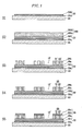
- FIGURE 1 is a schematic flowchart showing a method of making a plasma display panel according to one embodiment of the present invention.
- an address electrode 32 is formed on a front substrate 20 (S1).
- the substrate 20 may be a sheet-shaped insulating substrate, for example one made of glass, silicon, alumina, and so on, and is preferably a glass substrate.
- the insulating substrate may be subject to pretreatment such as a reagent treatment with a silane coupling agent, a plasma treatment, or thin membrane formation using an ion plating method, a sputtering method, a vapor reaction method, a vacuum deposition method, etc.
- the address electrode 32 may include a protrusion electrode 32a and a bus electrode 32b.
- the protrusion electrode 32a may be a transparent electrode, for example an ITO (Indium Tin Oxide) electrode that is suitable for forming an opening of a panel.
- the bus electrode 32b may be a metal electrode such as Ag to compensate a high resistance of the transparent electrode and thereby improve conductivity thereof.
- the protrusion electrode and the bus electrode may be formed in accordance with a conventional method.
- the protrusion electrode 32a may be formed using a photo etching method. More particularly, ITO is sputtered on a substrate, a dry film register (hereinafter referred to as "DFR") is laminated thereon, and then the DFR is patterned by exposure and development in accordance with the shape of the protrusion electrode. Subsequently, etching is performed and the DFR pattern is peeled off followed by firing to form a protrusion electrode 32a.
- DFR dry film register
- the bus electrode 32b may be formed using a photosensitive paste method. More particularly, a photosensitive paste for forming a bus electrode including Ag is coated, followed by leveling and drying. Subsequently, it is exposed, which can be performed by indirect exposure using a photo mask or by direct exposure. The drying and exposure are repeated three times or more, followed by development and firing to form a bus electrode 32b with a predetermined pattern.
- the green sheet 280 has a double-layered structure including a first green sheet layer 280a made of a composition for a first dielectric layer, and a second green sheet layer 280b which is formed on the first green sheet layer and is made of a photosensitive composition for a second dielectric layer.
- the composition for a first dielectric layer may be a general composition for forming a dielectric layer and is not particularly limited. It may include lead-free glass powders which are preferably not harmful to the environment or people. Non-limiting examples of the glass powder include at least one selected from the group consisting of ZnO, B 2 O 3 , Al 2 O 3 , SiO 2 , SnO, P 2 O 5 , Sb 2 O 3 , and Bi 2 O 3 .
- it may include at least one selected from the group consisting of zinc oxide-boron oxide-silicon oxide (ZnO-B 2 O 3 -SiO 2 ), zinc oxide-boron oxide-silicon oxide-aluminum oxide (ZnO-B 2 O 3 -SiO 2 -Al 2 O 3 ), bismuth oxide-boron oxide-silicon oxide (Bi 2 O 3 -B 2 O 3 -SiO 2 ), bismuth oxide-boron oxide-silicon oxide-aluminum oxide (Bi 2 O 3 -B 2 O 3 -SiO 2 -Al 2 O 3 ), bismuth oxide-zinc oxide-boron oxide-silicon oxide (Bi 2 O 3 -ZnO-B 2 O 3 -SiO 2 ), and bismuth oxide-zinc oxide-boron oxide-silicon oxide-aluminum oxide (Bi 2 O 3 -ZnO-B 2 O 3 -SiO 2 ), and bismuth oxide-zinc oxide-
- the glass powder may include at least one selected from the group consisting of oxides of Group 1 to Group 5 metal elements, oxides of lanthanum-based elements, and fluorides of Group 1 metal elements.
- the glass powder may include at least one selected from the group consisting of Na 2 O, Li 2 O, K 2 O, Cs 2 O, MgO, CaO, SrO, BaO, Sc 2 O 3 , Y 2 O 3 , TiO 2 , ZrO 2 , V 2 O 5 , Nb 2 O 5 , La 2 O 3 , CeO 2 , Pr 2 O 3 , Nd 2 O 3 , Sm 2 O 3 , Eu 2 O 3 , Gd 2 O 3 , Tb 2 O 3 , Dy 2 O 3 , Ho 2 O 3 , Er 2 O 3 , Tm 2 O 3 , Yb 2 O 3 , Lu 2 O 3 , LiF, NaF, and KF.
- the Group 1 to Group 5 metal elements refer to the element of Group 1 to Group 5 of the
- the glass powder is prepared by mixing all the components, and fusing, dry cooling, dry pulverizing, and crushing them.
- the glass powder prepared according to the method has good fineness and color.
- the glass powder is not limited to any shape thereto, but a spherical shape is preferable. It has an average particle diameter ranging from 0.1 to 5 ⁇ m, and is preferably 0.5 to 2 ⁇ m. When the average particle diameter of the glass powder is out of the above range, the surface of the dielectric layer pattern formed after firing is non-uniform and the linearity of the pattern may be reduced.
- the composition for a first dielectric layer may include 50 to 70wt%, and preferably 55 to 65wt%, of the glass powder based on the total weight of the composition for the first dielectric layer.
- amount of the glass powder is less than 50wt%, greater amounts of a binder and a plasticizer are needed and thus sintering characteristics of the composition may be deteriorated.
- it is more than 70wt%, relative amounts of a binder and a plasticizer are reduced and thus it is hard to handle and work with.
- the composition for a first dielectric layer may include a balance amount of a solvent, a binder, or a plasticizer, which are generally used in forming a dielectric layer.
- the photosensitive composition for a second dielectric layer includes i) a glass powder, ii) a photosensitive binder, iii) a cross-linking compound having at least two ethylene-based double bonds, iv) a photopolymerization initiator, and v) a solvent.
- the glass powder is the same as one used in the composition for a first dielectric layer.
- the photosensitive composition for a second dielectric layer may include 50 to 65wt%, and preferably 55 to 60wt%, of a glass powder based on a total weight of the photosensitive composition for the second dielectric layer.
- amount of the glass powder is less than 50wt%, sintering characteristics of the composition may be deteriorated.
- it more than 65wt% it is hard to handle and work with.
- the photosensitive binder may be a polymer which can be cross-linked by a photoinitiator and can be easily removed by development during formation of a pattern of a dielectric layer.
- Such a photosensitive binder may be an acryl-based resin, a styrene resin, a novolac resin, or a polyester resin which is generally used in a photoresist composition.
- the photosensitive binder may be a polymer which is obtained by polymerizing at least monomer selected from the group consisting of a) a monomer having a carboxyl group, b) a monomer having a OH group, and c) another monomer that can be copolymerized.
- the monomer having a carboxyl group may include acrylic acid, methacrylic acid, maleic acid, fumaric acid, crotonic acid, itaconic acid, citraconic acid, mesaconic acid, cinamic acid, mono (2-(meth)acryloyloxyethyl) succinate, or ⁇ -carboxylpolycaprolactone mono(meth)acrylate.
- the monomer having an OH group may include 2-hydroxyethyl (meth)acrylate, 2-hydroxypropyl (meth)acrylate, 3-hydroxypropyl (meth)acrylate, a phenolic monomer having a OH group such as o-hydroxystyrene, m-hydroxystyrene, p-hydroxystyrene, and so on.
- Another monomer that can be copolymerized may include a (meth)acrylic acid ester such as methyl (meth)acrylate, ethyl (meth)acrylate, n-butyl (meth)acrylate, n-lauryl (meth)acrylate, benzyl (meth)acrylate, glycidyl (meth)acrylate, dicyclopentanyl (meth)acrylate, phosphate acrylate; an aromatic vinyl-based monomer such as styrene, ⁇ -methylstyrene, and so on; a conjugated diene such as butadiene, isoprene, and so on; a macromonomer (polymer) having a polymerizable unsaturated group such as a (meth)acryloyl group at one end of a polymer chain, such as polystyrene, poly(methyl (meth)acrylate), poly(ethyl (meth)acrylate), poly(benzyl (
- the photosensitive binder has a number average molecular weight (Mn) ranging from 5,000 to 50,000, so that it may have a suitable viscosity for coating the photosensitive composition for a second dielectric layer on a substrate and may be decomposed during a development process.
- Mn number average molecular weight
- the photosensitive binder has an acid value ranging from 20 to 100mg KOH/g. When the acid value is less than 20mg KOH/g, it is hard to dissolve in an alkali aqueous solution which causes a failure of development. When it is more than 100mg KOH/g, the photosensitive dielectric layer cannot be closely attached during the development process, or exposed portions may dissolve.
- the photosensitive binder may be used in an amount of 5 to 10wt%, and preferably at 5 to 7wt% based on the total weight of the photosensitive composition for a second dielectric layer.
- amount of the photosensitive binder is less than 5wt%, printing properties are poor, whereas when it is more than 10wt%, development failure may be caused or residue may remain around a dielectric layer after firing.
- the cross-linking compound having at least two ethylene-based double bonds is any compound to which a radical polymerization reaction can be performed by a photoinitiator, and it is not particularly limited.
- it may include an acrylate, a methacrylate, or a mono-, di-, tri- or more ester which is obtained by a reaction of a polybasic acid and hydroxy alkyl(meth)acrylate.
- the polybasic acid may include phthalic acid, adipic acid, maleic acid, itaconic acid, trimellitic acid, terephthalic acid, and so on.
- the listed monomer may be used singularly, in combination or in a copolymer.
- the cross-linking compound may be at least one selected from the group consisting of 1,4-butanedioldiacrylate, 1,3-butylene glycol diacrylate, ethylene glycol diacrylate, pentaerythrytol tetraacrylate, triethylene glycol diacrylate, dipentaerythrytol diacrylate, sorbitol triacrylate, a bisphenol A diacrylate derivative, trimethylol propane triacrylate, trimethylol propane triacrylate modified with ethylene oxide, dipentaerythrytol polyacrylate, 1,4-butanediol dimethacrylate, 1,3-butylene glycol dimethacrylate, ethylene glycol dimethacrylate, pentaerythrytol tetramethacrylate, triethylene glycol dimethacrylate, dipentaerythrytol dimethacrylate, sorbitol trimethacrylate, bisphenol A dimethacrylate derivative, trimethylol propanetrimeth
- the cross-linking compound is added in a predetermined ratio based on the amount of the photosensitive binder. It may be added in an amount of 20 to 150 parts by weight based on 100 parts by weight of the photosensitive binder.
- the amount of the cross-linking compound is calculated based on the photosensitive composition for a second dielectric layer, the amount corresponds to 1 to 15 wt%, and preferably 3 to 10wt% based on the total weight of the photosensitive composition for a second dielectric layer.
- the amount of the cross-linking compound is less than 1wt%, exposure sensitivity may be reduced during exposure for forming a dielectric layer, and a defect in a dielectric layer pattern may be formed during development.
- it is more than 15wt% excessive cross-linking may occur and thereby a rough pattern may be formed after development, and pattern linearity may be reduced.
- the photopolymerization initiator may include any compound that generates radicals during an exposure process, and that initiates a cross-linking reaction of the cross-linking compound, and it is not particularly limited.
- Typical examples of the photopolymerization initiator include benzoin, benzoin alkyl ethers such as benzoin methylether, benzoin ethylether, or benzoin isopropylethyl; acetophenone-based compounds such as acetophenone, 2,2-dimethoxy-2-phenylacetophenone, 2,2-diethoxy-2-phenylacetophenone, 1,1-dichloroacetophenone; aminoacetophenones such as ⁇ -amino acetophenone, 2-methyl-1-[4-(methylthio)phenyl]-2-morpholinopropanone-1,2-benzyl-2-dimethylamino-1- (4-morpholinophenyl)-butanone-1; anthraquinones such as 2-methylanthra
- ⁇ -amino acetophenone (Irgacure907 ® Ciba Specialty Chemicals Ltd.) may be used.
- the photopolymerization initiator is added in a predetermined ratio based on the amount of the cross-linking compound. It may be added in an amount of 10 to 50 parts by weight based on 100 parts by weight of the cross-linking compound.
- the amount of the photopolymerization initiator is calculated based on the photosensitive composition for a second dielectric layer, the amount corresponds to 0.1 to 8wt%, and preferably 0.3 to 5wt%, based on the total weight of the photosensitive composition for a second dielectric layer.
- the amount of the photopolymerization initiator is less than 0.1wt%, exposure sensitivity may be reduced and it is difficult to obtain a good pattern, and linearity of a pattern may be reduced.
- it is more than 8wt% storage stability may be reduced and excessive cross-linking may occur and thereby a rough pattern may be formed after development.
- the photosensitive composition for a second dielectric layer includes a solvent to improve coating of the composition.
- Suitable solvents may be selected depended on dissolution and coating properties of the components of the photosensitive composition for the second dielectric layer.
- Typical examples include ketones such as diethylketone, methylbutylketone, dipropylketone, cyclohexanone, and so on; alcohols such as n-pentenol, 4-methyl-2-pentenol, cyclohexanol, diacetonealcohol, and so on; ether-based alcohols such as ethylene glycol monomethylether, ethylene glycol monoethylether, ethylene glycol monobutylether, propylene glycol monomethylether, propylene glycol monoethylether, and so on; saturated aliphatic monocarboxylic acid alkyl esters such as n-butyl acetate and amyl acetate; lactic acid esters such as ethyl lactate, n-butyl lactate, and so on; and ether-based esters such as methylcello
- the solvent may be used in a balance amount of the photosensitive composition for a second dielectric layer. It may be used in an amount of 4 to 30wt%, and preferably 10 to 25wt% based on the total weight of the photosensitive composition for a second dielectric layer to obtain a composition having a suitable viscosity.
- the photosensitive composition for a second dielectric layer may include an additive depending on properties of the composition to be obtained.
- the additive may include a sensitizer for improving sensitivity; a polymerization inhibitor for improving storage stability of a coating composition, such as phosphoric acid, phosphoric acid ester, or a carboxylic acid-containing compound; an oxidation inhibitor; an ultraviolet ray absorber for improving resolution; an antifoaming agent for reducing pores in a coating composition such as a silicon-based or acryl-based compound; a dispersing agent for improving dispersion properties; a leveling agent for improving flatness of a printed layer, such as polyester modified dimethylpolysiloxane, polyhydroxycarboxylic acid amide, a silicon-based polyacrylate copolymer, or a fluoro-based paraffin compound; or a plasticizer for endowing thixotropy characteristics.
- the additive may be added as needed in a suitable amount.
- the photosensitive composition for a second dielectric layer is prepared by dispersing glass powders, a photosensitive binder, a cross-linking compound having at least two ethylene-based double bonds, and a photopolymerization initiator in a solvent.
- the photosensitive binder and the photopolymerization initiator are mixed first, and then the glass powder, cross-linking compound, and solvent are added to disperse the mixture.
- compositions for a first dielectric layer and the photosensitive composition for a second dielectric layer may be coated on a supporter such as polyethyleneterephthalate film using a general coating method such as knife coating or die coating, and then dried to remove a solvent. Thereby, a film-shaped first green sheet layer 280a and the second green sheet layer 280b are formed. The first green sheet layer 280a and the second green sheet layer 280b are stacked to each other to make a green sheet 280.
- the first green sheet layer 280a may be thicker than the second green sheet layer 280b.
- the first green sheet layer 280a and the second green sheet layer 280b may be formed in a thickness ratio ranging 3:1 to 4:1.
- cost may increase and a high-definition pattern may be difficult to obtain.
- the second green sheet layer 280b has a thickness ranging from 5 to 30 ⁇ m, preferably 8 to 25 ⁇ m, and more preferably 10 to 20 ⁇ m when considering a thickness of a display electrode of a plasma display panel.
- the green sheet 280 is laminated on a substrate 20 on which an address electrode 32 is formed, then the green sheet 280 is subject to exposure and development, and is fired to form a pattern of a dielectric layer 28 (S3).
- the exposure may be performed with respect to the photosensitive second green sheet layer 280b.
- the exposure may be performed by optionally radiating UV rays to the second green sheet layer 280b through a patterned photomask. Alternatively, it can be performed in a direct imaging (DI) manner.
- DI direct imaging
- halogen lamps high pressure mercury lamps, laser lights, metal halogen lamps, black lamps, electrodeless lamps, and so on may be used.
- the exposing amount ranges from 50 to 1,000mJ/cm 2 .
- the development solution may be a base aqueous solution.
- the base may be selected from the group consisting of an inorganic alkali compound such as lithium hydroxide, sodium hydroxide, potassium hydroxide, phosphoric acid hydrogen sodium, phosphoric acid hydrogen diammonium, phosphoric acid hydrogen dipotassium, phosphoric acid hydrogen disodium, phosphoric acid dihydrogen ammonium, phosphoric acid dihydrogen potassium, phosphoric acid dihydrogen sodium, lithium silicate, sodium silicate, potassium silicate, lithium carbonate, sodium carbonate, potassium carbonate, lithium borate, sodium borate, potassium borate, ammonia, and so on; and an organic alkali compound such as tetramethyl ammonium hydroxide, trimethyl hydroxyl ethyl ammonium hydroxide, monomethylamine, dimethylamine, trimethylamine, monoethylamine, diethylamine, triethylamine, mono
- the development solution has a concentration ranging 0.1 to 1%, and is preferably 0.2 to 0.6%.
- concentration is less than 0.2%, the time for forming a pattern is lengthened, whereas when it is more than 1%, pattern uniformity is reduced.
- the development solution has a temperature ranging from 25°C to 55°C, and is preferably 30°C to 45°C. When the temperature is less than 25°C, development time increases, whereas when it is more than 40°C, a process margin for forming a pattern decreases.
- the photopolymerization initiator is exposed to ultraviolet rays and decomposed to generate free radicals.
- the active radicals attack a double bond of the cross-linking compound to induce a polymerization reaction.
- the cross-linking compound has at least two double bonds in one molecule and thereby forms a polymer having a three dimensional network structure through a polymerization reaction.
- the polymer is not removed by the development solution.
- the non-exposed portions When the photosensitive binder of the non-exposed portions is dissolved out by an alkali aqueous solution during development, the glass powder and unreacted cross-linking compound are removed together. Thereby, the non-exposed portions have a different shape to that of the exposed portions to form a patterned second dielectric layer 28b.
- any unnecessary development solution may be removed by rinsing or performing neutralization with acid.
- the patterned second dielectric layer 28b is fired.
- spaces 21' and 24' for forming display electrodes and a discharge cell 18' are formed in the second dielectric layer 28b simultaneously.
- the firing process may be performed at a temperature ranging from 480°C to 620°C, and preferably at 500°C to 580°C. It is performed for 3 to 6 hours, and preferably for 4 to 5 hours. When the firing temperature and time are out of the range, moisture is not completely removed, and binder is also not removed completely.
- a composition for forming a display electrode is filled in the pattern of the dielectric layer followed by firing to form a patterned display electrode (S4). More specifically, a composition for forming a display electrode is filled in spaces for forming display electrodes 21' and 23' between the patterns of the second dielectric layer 28b and fired to form a display electrode 25 including a sustain electrode 21 and a scan electrode 23.
- the composition for forming a display electrode may be a composition which is generally used for making a display electrode, without limitation.
- the composition may include at least one metal selected from the group consisting of silver (Ag), gold (Au), aluminum (A1), copper (Cu), nickel (Ni), chromium (Cr), and a silver-palladium alloy (Ag-Pd).
- the firing process during forming a patterned display electrode may be performed at a temperature of 500°C to 600°C, and preferably at 550°C to 580°C.
- the firing time may range from 3 to 6 hours, and is preferably 4 to 5 hours. When the firing temperature and time are out of the range, pores may be formed.
- a third dielectric layer 28c is formed to cover the display electrode 25 (S5).
- a composition for a third dielectric layer is coated to cover the display electrode 25 followed by firing to form the third dielectric layer 28c.
- the third dielectric layer 28c may be extended to cover the second dielectric layer 28b as well as the display electrode 25.
- the third dielectric layer may be formed using a general coating composition for a first dielectric layer and a coating method. More preferably, the third dielectric layer may be formed using the same composition as the composition for the first dielectric layer.
- a protection layer may additionally be formed to cover the dielectric layer formed on the display electrode.
- the protection layer may include at least one layer selected from the group consisting of a fluoride layer and an oxide layer. More specifically, the protection layer may include a fluoride compound such as MgF 2 , CaF 2 , or LiF; and an oxide compound such as MgO, Al 2 O 3 , ZnO, CaO, SrO, SiO 2 , or La 2 O 3 .
- the protection layer may be formed with any a thick-layer printing method using a paste or a deposition method using a plasma, but the method is not limited to thereto.
- the protection layer formed by the deposition method has relatively good resistance to ion impacts, and can release secondary electrons to thereby reduce a discharge maintenance voltage and discharge initiation voltage.
- the plasma deposition method may include a magnetron sputtering method, electron beam deposition, IBAD (ion beam assisted deposition), CVD (chemical vapor deposition), an ion plating method, and so on.
- barrier ribs and phosphor layers may be formed successively in accordance with a conventional process.
- the fabricated rear substrate and the front substrate are assembled with each other, followed by evacuating and sealing them to make a plasma display panel.
- a dielectric layer to cover an address electrode and a dielectric layer covering display electrodes are formed in a singular process using two-layer green sheet, which thereby simplifies a manufacturing process and reduces manufacturing time and inferior products.
- the present invention also provides a method of making a plasma display panel.
- FIGURE 2 is a schematic exploded perspective view showing a plasma display panel in accordance with one embodiment of the present invention.
- the plasma display panel includes a rear substrate 10 and a front substrate 20 which are disposed to be opposed to each other with a predetermined interval therebetween, and a plurality of discharge cells 18 and 18' separated by the barrier ribs 16 between the two substrates 10 and 20.
- Phosphor layers 19 to absorb ultraviolet rays and release visible rays are formed on the sidewalls of the barrier ribs 16 and the bottom surfaces of discharge cells 18 and 18' in which discharge gases, for example a mixed gas of xenon (Xe), neon (Ne), etc. are filled, to cause a plasma discharge.
- discharge gases for example a mixed gas of xenon (Xe), neon (Ne), etc.
- Address electrodes 32 are disposed on the front substrate 20 along one direction (y-axis direction of the drawing).
- a dielectric layer 28 is disposed on the entire interior surface of the front substrate 20 so as to cover the address electrodes 32.
- the neighboring address electrodes 32 are arranged with a predetermined interval therebetween.
- Each of the address electrodes 32 includes a protrusion electrode 32a and a bus electrode 32b.
- the bus electrode 32b extends along one edge of the discharge cells 18 and 18'.
- the protrusion electrode 32a protrudes from the bus electrode 32b toward the opposite edge of the discharge cells 18 and 18'.
- the protrusion electrode 32a is a transparent electrode made of, for example, indium tin oxide (ITO) in order to increase the aperture ratio of the panel.
- the bus electrode 32b is preferably a metallic electrode to increase the conductivity of the bus electrode 32b by compensating for a high resistance of the protrusion electrode 32a.
- the protrusion electrode 32a may have preferably a rectangular shape.
- Display electrodes 25 are disposed in proximity to the address electrodes 32.
- the display electrodes 25 are electrically isolated and separated from the address electrodes 32 by a front dielectric layer 28.
- Each of the display electrodes 25 in a respective discharge cell includes a sustain electrode 21 and a scan electrode 23.
- the sustain electrode 21 and scan electrode 23 extend in a direction (the x direction in the drawing) intersecting the address electrode 32.
- the sustain electrodes 21 are used to apply a discharge voltage during a sustain period.
- the scan electrodes 23 are used to apply discharge voltages in reset, address, and sustain periods.
- the scan electrodes 23 are involved in all of the discharges of the reset, address, and sustain periods.
- the sustain electrodes 21 are mainly involved in discharge during the sustain period.
- the functions of the electrodes vary according to the discharge voltages applied to the electrodes. Therefore, the electrodes are not limited to the aforementioned functions.
- the respective pair of sustain and scan electrodes are disposed in one discharge cell in FIGURE 2.
- the sustain or scan electrodes may be disposed in the boundary of neighboring discharge cells, the sustain or scan electrode thereby being used for both neighboring discharge cells.
- the sustain electrode 21 and the scan electrode 23 protrude in a direction (the opposite direction of z direction in the drawing) from the front substrate 20 to the rear substrate 10.
- the sustain electrode 21 and the scan electrode 23 face each other so as to define a space therebetween. A facing discharge is generated in the space between the sustain electrode 21 and the scan electrode 23.
- the sustain electrodes 21, the scan electrodes 23, and the address electrodes 32 are formed in different layers and are electrically isolated by a dielectric layer 28.
- the dielectric layer 28 includes a first dielectric layer 28a, a second dielectric layer 28b, and a third dielectric layer 28c.
- the first dielectric layer 28a is formed so as to cover the address electrodes 32 in the front substrate 20.
- the second dielectric layer 28b is formed so as to surround the sustain electrodes 21 and scan electrodes 23, which are the display electrodes 25 disposed on the first dielectric layer 28a.
- the third dielectric layer 28c is formed so as to cover a display electrode 25 exposed to the discharge cell.
- the first dielectric layer 28a is formed using the first green sheet layer prepared from a composition for a first dielectric layer.
- the second dielectric layer 28b is formed using the second green sheet layer prepared from a photosensitive composition for a second dielectric layer.
- the second green sheet layer is formed on the first green sheet layer and then exposure, development, and firing are performed. During the above process, the photosensitive components are reacted in the second green sheet layer to form a dielectric layer pattern. Subsequently a composition for a display electrode is filled in the dielectric layer pattern to form a patterned display electrode.
- the third dielectric layer 28c may be formed so as to cover the display electrode 25 disposed toward to a discharge cell.
- the third dielectric layer 28c may be formed using the same composition as the composition for the first dielectric layer 28a in accordance with a conventional method.
- a MgO protection layer 29 may be formed on the first dielectric layer 28a, the second dielectric layer 28b, and the third dielectric layer 28c in order to protect them from the impact of ions during the plasma discharge. In addition, since it has a high secondary electron emission coefficient with respect to the impacting ions, the protective layer 29 can improve discharge efficiency.
- barrier ribs 16 are disposed on the rear substrate 10.
- the barrier ribs 16 include first barrier rib members 16a and second barrier rib members 16b.
- the first barrier rib members 16a extend in a direction parallel to the address electrode 32, and the second barrier rib members 16b intersect the first barrier rib member 16a and compartmentalize each discharge cell 18 and 18' to be an independent space.
- the barrier ribs may be disposed in various structures, such as stripe and matrix structures. In the stripe structure, longitudinal barrier ribs are disposed parallel to each other and to address electrodes. In the matrix structure, each discharge cell is partitioned to be an independent cell. As shown in FIGURE 2, a dielectric layer 14 may be formed on the rear substrate 10.
- all of the electrodes associated with discharge in the discharge cells 18 are disposed on the front substrate 20.
- the address electrodes 32 and the display electrodes 25 are disposed on the front substrate 20.
- the discharge space partitioned by the barrier ribs 16 can increase.
- the area of the coated phosphor layers can increase so that discharge efficiency can be improved.
- the associated accumulation of charge on the phosphor layers can prevent shortening of the life-span of the phosphor layers due to ion sputtering.
- a first green sheet layer was prepared by coating a polyethyleneterephthalate supporter with a composition for a first dielectric layer, which included a glass powder of SiO 2 -ZnO-B 2 O 3 with an average particle diameter of 1 ⁇ m (69.8wt% of SiO 2 , 28.4wt% of ZnO, and 1.8wt% of B 2 O 3 ), and then drying it to be 45 ⁇ m thick.
- a second green sheet layer was prepared by coating a polyethyleneterephthalate supporter with a composition for a second dielectric layer, which was prepared by dissolving 8wt% of an acrylate copolymer resin (22wt% of benzylmethacrylate, 25wt% of methacrylic acid, 7wt% of phosphateacrylate, 20wt% of 2-hydroxyethylmethacrylate, and 26wt% of methylmethacrylate based on the total weight of monomers), 10wt% of TMP(EO) 3 TA, and 2wt% of Irgacure 907 into 20wt% of PGMEA, and thereafter dispersing 60wt% of a glass powder of SiO 2 -ZnO-B 2 O 3 , and then drying it to be 15 ⁇ m thick.
- an acrylate copolymer resin 22wt% of benzylmethacrylate, 25wt% of methacrylic acid, 7wt% of phosphateacrylate,
- a green sheet was prepared by assembling the first green sheet layer with the second green sheet layer.
- Another green sheet was prepared according to the same method as in Preparation Example 1, except for using a glass powder of B 2 O 3 -BaO-ZnO with an average particle diameter of 0.1 ⁇ m (comprising 70wt% of B 2 O 3 , 20wt% of BaO, and 10wt% of ZnO) instead of the SiO 2 -ZnO-B 2 O 3 glass powder.
- a glass powder of B 2 O 3 -BaO-ZnO with an average particle diameter of 0.1 ⁇ m comprising 70wt% of B 2 O 3 , 20wt% of BaO, and 10wt% of ZnO
- a green sheet was prepared according to the same method as in Preparation Example 1, except for using a glass powder of Bi 2 O 3 -B 2 O 3 -SiO 2 -Al 2 O 3 -Na 2 O-MgO with an average particle diameter of 5 ⁇ m (25wt% of Bi 2 O 3 , 25wt% of B 2 O 3 , 30wt% of SiO 2 , 15wt% of Al 2 O 3 , 2wt% of Na 2 O, and 3wt% of MgO) instead of the SiO 2 -ZnO-B 2 O 3 glass powder.
- Example 1 Manufacture of a plasma display panel
- a front substrate made of soda lime glass was sputtered with indium tin oxide and a dry film register (DFR) was laminated thereon.
- a patterned photo mask was additionally laminated on the DFR, and thereafter it was exposed by using high pressure mercury lamp, developed by using a 0.4% Na 2 CO 3 alkali aqueous solution, and dried to pattern the DFR to have a shape corresponding to a protrusion electrode.
- protrusion electrodes were formed by etching the patterned substrate with hydrochloric acid and nitric acid, peeling the DFR patterned part with an aqueous solution containing 5.0% of NaOH, and then firing it.
- a photosensitive paste for forming a bus electrode including Ag was applied on the protrusion electrodes.
- the coated photosensitive paste including Ag was leveled, dried, and thereafter exposed by using a DI (direct imaging) exposer.
- bus electrodes having a stripe pattern were formed by repeating drying and exposing five times on the resultant substrate, developing it with a 0.4% Na 2 CO 3 aqueous solution, and firing it. Then, address electrodes including the protrusion electrodes and the bus electrodes were fabricated.
- the green sheet prepared in Preparation Example 1 was laminated on the substrate including the address electrode formed thereon. Thereafter, it was exposed 100mJ/cm 2 by using a DI (direct imaging) exposer, developed by spraying a 0.4% Na 2 CO 3 alkali aqueous solution thereon, and fired at 500°C for 4 hours to form a dielectric layer pattern.
- DI direct imaging
- the dielectric layer pattern was filled with a composition for forming a display electrode including Cr-Cu-Cr and fired at 500°C for 4 hours to form a patterned display electrode.
- a composition for a first dielectric layer which includes a glass powder of SiO 2 -ZnO-B 2 O 3 (69.8wt% of SiO 2 , 28.4wt% of ZnO, and 1.8wt% of B 2 O 3 ), was additionally coated on the patterned display electrode, and was dried and fired to form a dielectric layer.
- a rear substrate was formed with a patterned barrier rib and a phosphor layer. Then, it was assembled with the above fabricated front substrate formed with the address electrode, the display electrode, and the dielectric layer. Thereafter, the air in a discharge cell was evacuated, and discharge gases were injected under a condition of 400Torr to manufacture a resultant plasma display panel.
- Example 2 Manufacture of a plasma display panel
- a plasma display panel was manufactured according to the same method as in Example 1, with the exception of using the green sheet prepared in Preparation Example 2.
- Example 3 Manufacture of a plasma display panel
- a front substrate made of soda lime glass was sputtered with indium tin oxide, and a dry film register (DFR) was laminated thereon.
- a patterned photo mask was additionally laminated on the DFR, and thereafter the laminated substrate was exposed by using a high pressure mercury lamp, developed by using a 0.4% Na 2 CO 3 alkali aqueous solution, and dried to pattern the DFR to have a shape corresponding to a protrusion electrode.
- protrusion electrodes were formed by etching the patterned substrate with hydrochloric acid and nitric acid, peeling the DFR patterned part with an aqueous solution containing 5.0% of NaOH, and then firing it.
- a photosensitive paste for forming a bus electrode including Ag was applied on the protrusion electrodes of the front substrate.
- the coated photosensitive paste including Ag was leveled, dried, and thereafter exposed by using a DI (direct imaging) exposer.
- Bus electrodes with a stripe pattern were formed by repeating the drying and exposing five times on the resulting substrate, developing it by using a 0.4% Na 2 CO 3 alkali aqueous solution, and firing it. Then, address electrodes including the protrusion electrodes and the bus electrodes were fabricated.
- a green sheet prepared according to Preparation Example 3 was laminated on the substrate including the address electrode formed thereon, exposed 100mJ/cm 2 by using a DI (direct imaging) exposer, developed by using a 0.4% Na 2 CO 3 alkali aqueous solution, and fired at 500°C for 4 hours to form a dielectric layer pattern. Then, the dielectric layer pattern was filled with a composition for forming a display electrode including Cr-Cu-Cr and fired at 550°C for 4 hours to form a patterned display electrode.
- DI direct imaging
- the patterned display electrode was additionally coated with a composition for a third dielectric layer including a glass powder of Bi 2 O 3 -B 2 O 3 -SiO 2 -Al 2 O 3 -Na 2 O-MgO, dried, and fired to form a third dielectric layer.
- a front substrate was fabricated by putting the substrate with the dielectric layer in a protection layer deposition room and depositing a protection layer including MgO with an ion plating method.
- the deposition room was internally maintained to have a basic pressure of 1 ⁇ 10 -4 Pa and a pressure of 5.3 ⁇ 10 -2 Pa during the deposition, and was supplied with oxygen at 100sccm (a flux volume unit) to keep the substrate at 200 ⁇ 5°C.
- a plasma display panel was made by forming a barrier rib and a phosphor layer on a rear substrate, and assembling it with the above fabricated front substrate having an address electrode, a display electrode, and a dielectric layer. Thereafter, the air in a discharge cell was evacuated and discharge gases were injected into the discharge cell under a condition of 400Torr to manufacture a resultant plasma display panel.
- Comparative Example 1 Manufacture of a plasma display panel
- a front substrate made of soda lime glass was sputtered with indium tin oxide and a dry film register (DFR) was laminated thereon.
- a patterned photo mask was additionally laminated on the DFR, and thereafter it was exposed by using high pressure mercury lamp, developed by using a 0.4% Na 2 CO 3 alkali aqueous solution, and dried to pattern the DFR to have a shape corresponding to a protrusion electrode.
- protrusion electrodes were formed by etching the patterned substrate with hydrochloric acid and nitric acid, peeling the DFR patterned part with an aqueous solution containing 5.0% of NaOH, and then firing it.
- a photosensitive paste for forming a bus electrode including Ag was applied on the protrusion electrodes.
- the coated photosensitive paste including Ag was leveled, dried, and thereafter was exposed by using a DI (direct imaging) exposer.
- bus electrodes having a stripe pattern were formed by repeating drying and exposing five times on the resultant substrate, developing it with a 0.4% Na 2 CO 3 aqueous solution, and firing it. Then, address electrodes including the protrusion electrodes and the bus electrodes were fabricated.
- a first dielectric layer was formed by coating a composition for a first dielectric layer, which includes a glass powder of PbO-B 2 O 3 -SiO 2 , and drying and then firing it.
- the dielectric layer was coated with a composition for forming a display electrode including Cr-Cu-Cr in a screen-coating method. Then, a display electrode was formed by repeating the coating and drying process ten times.
- a dielectric layer pattern was formed by coating a photosensitive composition for a second dielectric layer, which was prepared by dissolving 8wt% of an acrylate copolymer resin (22wt% of benzylmethacrylate, 25wt% of methacrylic acid, 7wt% of phosphateacrylate, 20wt% of 2-hydroxyethylmethacrylate, and 26wt% of methylmethacrylate based on the entire monomer), 10wt% of TMP(EO)3TA, and 2wt% of Irgacure907 into 20wt%of PGMEA and thereafter dispersing 60wt% of a glass powder of PbO-B2O3-SiO2, and then drying, exposing, developing, and firing it.
- an acrylate copolymer resin 22wt% of benzylmethacrylate, 25wt% of methacrylic acid, 7wt% of phosphateacrylate, 20wt% of 2-hydroxyethylmeth
- a rear substrate was formed with a rear dielectric layer, a barrier rib, and a phosphor layer.
- the rear substrate was assembled with the front substrate with the address electrode, the display electrode, and the dielectric layer.
- a plasma display panel was fabricated by evacuating the air in a discharge cell and injecting a discharge gas thereinto under a condition of 400Torr.
- a dielectric layer to cover an address electrode and a dielectric layer covering display electrodes can be formed in a singular process using a two-layer green sheet, and it thereby simplifies a manufacturing process and reduces manufacturing time and inferior products.
Landscapes
- Chemical & Material Sciences (AREA)
- Engineering & Computer Science (AREA)
- Geochemistry & Mineralogy (AREA)
- Life Sciences & Earth Sciences (AREA)
- Chemical Kinetics & Catalysis (AREA)
- General Chemical & Material Sciences (AREA)
- Materials Engineering (AREA)
- Organic Chemistry (AREA)
- Physics & Mathematics (AREA)
- Plasma & Fusion (AREA)
- Manufacturing & Machinery (AREA)
- Ceramic Engineering (AREA)
- Dispersion Chemistry (AREA)
- Gas-Filled Discharge Tubes (AREA)
- Materials For Photolithography (AREA)
Abstract
Description
- The present invention relates to a method of making a plasma display panel. More particularly, the present invention relates to a method of making a plasma display panel in which a dielectric layer to cover an address electrode and a dielectric layer covering display electrodes are formed in a singular process using a two-layer green sheet, and which thereby simplifies a manufacturing process and reduces manufacturing time and inferior products.
- A plasma display panel (herein referred to as a "PDP") is a display apparatus using plasma discharge. Vacuum ultraviolet (herein referred to as "VUV") rays emitted by the plasma discharge excite phosphor layers, and in turn, the phosphor layers emit visible light. The visible light is used to display images. Recently, the PDP has been implemented as a thin wide screen apparatus having a screen size of 60 inches or more and a thickness of 10 cm or less. In addition, since it is a spontaneous light emitting apparatus like a cathode ray tube (CRT), the PDP has excellent color reproducibility. Further, the PDP has no image distortion associated with its viewing angle.
- Moreover, the PDP can be manufactured by a simpler method than a liquid crystal display (LCD) can, so the PDP can be produced with a low production cost and high productivity. Therefore, the PDP is expected to be the next generation of flat display apparatus for industry and home televisions.
- Since the 1970s, various structures of the PDP have been developed. In recent years, a three-electrode surface-discharge type PDP has been widely used. In the three-electrode surface-discharge PDP, two electrodes including scan and sustain electrodes are disposed on one substrate, and one address electrode is disposed on the other substrate in a direction intersecting the scan and sustain electrodes. The two substrates are separated from each other so as to provide a discharge cell. The discharge cell is filled with a discharge gas. In general, in the three-electrode surface-discharge PDP, the presence of a discharge is determined by an address discharge. Specifically, the address discharge is generated as a facing discharge between the scan electrode controlled separately and the address electrode opposite to the scan electrode, and a sustain discharge related to brightness is generated as a surface discharge between the scan and sustain electrodes disposed on the same substrate.
- A general AC three-electrode surface-discharge PDP includes a front substrate and a rear substrate facing each other. Address electrodes are disposed on the rear substrate along one direction, and a dielectric layer is disposed on the entire the front substrate so as to cover the address electrodes. A plurality of barrier ribs are disposed on the dielectric layer so as to define discharge cells. Red (R), green (G), and blue (B) phosphor layers are disposed in the respective discharge cells partitioned by the barrier ribs. Pairs of display electrodes are disposed on the front substrate in a direction intersecting the direction of address electrodes. Each pair of display electrodes includes a transparent electrode and a bus electrode. A dielectric layer and a protection layer made of magnesium oxide (MgO) are sequentially formed on the entire surface of the front substrate so as to cover the display electrodes. The intersections between the address electrodes of the rear substrate and the pairs of display electrodes correspond to the discharge cells.
- A metal electrode in such a structure of a plasma display panel is generally formed using a pattern-printing method. The pattern-printing method is relatively simple and can make a metal electrode with narrow intervals. However, there is a limit for forming a fine width of electrodes, and the method is not suitable for large screens and the high-definition of high resolution PDPs.
- The present invention is intended to provide a method of making a plasma display panel which simplifies the manufacturing process, and reduces manufacturing time and inferior products.
- According to a first aspect of the present invention, a method of making a plasma display panel includes the following steps. An address electrode is formed on a front substrate, a green sheet is formed to cover the address electrode, a dielectric layer pattern is formed by exposing, developing, and firing the green sheet, a composition for a display electrode is filled in the dielectric layer pattern and then fired to form a patterned display electrode, and a dielectric layer is formed to cover the patterned display electrode. The green sheet includes a first green sheet layer that is formed using a dielectric composition (i.e., a composition for a first dielectric layer), and a second green sheet layer that is formed on the first green sheet layer and that uses a photosensitive dielectric composition (i.e., a photosensitive composition for a second dielectric layer).
- The composition for a first dielectric layer may include 50 to 70wt% of a glass powder with respect to the total weight of the composition for the first dielectric layer.
- The glass powder may include at least one selected from the group consisting of ZnO, B2O3, Al2O3, SiO2, SnO, P2O5, Sb2O3, and Bi2O3. The glass powder may further include at least one material selected from the group consisting of oxides of group 1 to
group 5 metal elements, oxides of lanthanum-based elements, and fluorides of group 1 metal elements. - The photosensitive composition for the second dielectric layer may include a glass powder, a photosensitive binder, a cross-linking compound having at least two ethylene-based double bonds, a photopolymerization initiator, and a solvent. According to an embodiment of the present invention, a method of making a plasma display panel includes the following steps. An address electrode is formed on a front substrate, a green sheet is formed to cover the address electrode, a dielectric layer pattern is formed by exposing, developing, and firing the green sheet, a composition for a display electrode is filled in the dielectric layer pattern and then fired to form a patterned display electrode, a dielectric layer is formed to cover the patterned display electrode, thereby fabricating a front substrate, a patterned barrier rib is formed on a rear substrate, phosphor layers are formed on the barrier rib, and the fabricated front substrate and rear substrate are assembled, evacuated, and sealed. The green sheet includes a first green sheet layer that is formed using a composition for a first dielectric layer, and a second green sheet layer that is formed on the first green sheet layerand that uses a photosensitive composition for a second dielectric layer.
- According to a second aspect of the present invention, a green sheet for forming dielectric layers of a plasma display panel, including a first green sheet layer comprising a dielectric composition and a second green sheet layer formed on the first green sheet layer, and the second green sheet layer comprising a photosensitive dielectric composition.
- According to another aspect of the invention, there is provided the use of a green sheet according to the invention in its second aspect for making a plasma display panel.
- A more complete appreciation of the present invention, and many of the above and other features and advantages of the present invention, will be readily apparent as the same becomes better understood by reference to the following detailed description when considered in conjunction with the accompanying drawings in which like reference symbols indicate the same or similar components, wherein:
- FIGURE 1 is a schematic flowchart showing a method of making a plasma display panel according to one embodiment of the present invention; and
- FIGURE 2 is a schematic exploded perspective view showing a plasma display panel according to one embodiment of the present invention.
- Generally, an electrode of a plasma display panel with a predetermined height has been formed using a printing method. However, the printing method should be performed repeatedly to obtain the predetermined height or more. Therefore, more working processes are needed, and it is difficult to obtain a desirable pattern since each working process is not performed uniformly.
- In the present invention, a 2-layered green sheet is used to form a dielectric layer. The green sheet includes a first green sheet layerthat is formed using a composition for a first dielectric layer, and a second green sheet layer that is formed on the first green sheet layer and that uses a photosensitive composition for a second dielectric layer. Thereby, formation of a dielectric layer on an address electrode and another dielectric layer to cover a display electrode are performed in a single step. Display electrodes with the same height and shape can also be formed easily.
- According to an embodiment of the present invention, a method of making a plasma display panel includes the following steps:
- an address electrode is formed on a front substrate (S1);
- a green sheet is formed to cover the address electrode (S2);
- a dielectric layer pattern is formed by exposing, developing, and firing the green sheet (S3);
- a composition for a display electrode is filled in the dielectric layer pattern and then fired to form a patterned display electrode (S4); and
- a dielectric layer is formed to cover the patterned display electrode (S5).
- The green sheet includes a first green sheet layer that is formed using a composition for a first dielectric layer and a second green sheet layer that is formed on the first green sheet layer and that uses a photosensitive composition for a second dielectric layer.
- FIGURE 1 is a schematic flowchart showing a method of making a plasma display panel according to one embodiment of the present invention.
- Referring to FIGURE 1, an
address electrode 32 is formed on a front substrate 20 (S1). - The
substrate 20 may be a sheet-shaped insulating substrate, for example one made of glass, silicon, alumina, and so on, and is preferably a glass substrate. The insulating substrate may be subject to pretreatment such as a reagent treatment with a silane coupling agent, a plasma treatment, or thin membrane formation using an ion plating method, a sputtering method, a vapor reaction method, a vacuum deposition method, etc. - The
address electrode 32 may include aprotrusion electrode 32a and abus electrode 32b. Theprotrusion electrode 32a may be a transparent electrode, for example an ITO (Indium Tin Oxide) electrode that is suitable for forming an opening of a panel. Thebus electrode 32b may be a metal electrode such as Ag to compensate a high resistance of the transparent electrode and thereby improve conductivity thereof. - The protrusion electrode and the bus electrode may be formed in accordance with a conventional method.
- For example, the
protrusion electrode 32a may be formed using a photo etching method. More particularly, ITO is sputtered on a substrate, a dry film register (hereinafter referred to as "DFR") is laminated thereon, and then the DFR is patterned by exposure and development in accordance with the shape of the protrusion electrode. Subsequently, etching is performed and the DFR pattern is peeled off followed by firing to form aprotrusion electrode 32a. - The
bus electrode 32b may be formed using a photosensitive paste method. More particularly, a photosensitive paste for forming a bus electrode including Ag is coated, followed by leveling and drying. Subsequently, it is exposed, which can be performed by indirect exposure using a photo mask or by direct exposure. The drying and exposure are repeated three times or more, followed by development and firing to form abus electrode 32b with a predetermined pattern. - Then a
green sheet 280 is formed on the address electrode 32to cover the address electrode (S2). - The
green sheet 280 has a double-layered structure including a firstgreen sheet layer 280a made of a composition for a first dielectric layer, and a secondgreen sheet layer 280b which is formed on the first green sheet layer and is made of a photosensitive composition for a second dielectric layer. - The composition for a first dielectric layer may be a general composition for forming a dielectric layer and is not particularly limited. It may include lead-free glass powders which are preferably not harmful to the environment or people. Non-limiting examples of the glass powder include at least one selected from the group consisting of ZnO, B2O3, Al2O3, SiO2, SnO, P2O5, Sb2O3, and Bi2O3.
- According to the preferred embodiment of the present invention, it may include at least one selected from the group consisting of zinc oxide-boron oxide-silicon oxide (ZnO-B2O3-SiO2), zinc oxide-boron oxide-silicon oxide-aluminum oxide (ZnO-B2O3-SiO2-Al2O3), bismuth oxide-boron oxide-silicon oxide (Bi2O3-B2O3-SiO2), bismuth oxide-boron oxide-silicon oxide-aluminum oxide (Bi2O3-B2O3-SiO2-Al2O3), bismuth oxide-zinc oxide-boron oxide-silicon oxide (Bi2O3-ZnO-B2O3-SiO2), and bismuth oxide-zinc oxide-boron oxide-silicon oxide-aluminum oxide (Bi2O3-ZnO-B2O3-SiO2-Al2O3).
- The glass powder may include at least one selected from the group consisting of oxides of Group 1 to
Group 5 metal elements, oxides of lanthanum-based elements, and fluorides of Group 1 metal elements. According to one embodiment, the glass powder may include at least one selected from the group consisting of Na2O, Li2O, K2O, Cs2O, MgO, CaO, SrO, BaO, Sc2O3, Y2O3, TiO2, ZrO2, V2O5, Nb2O5, La2O3, CeO2, Pr2O3, Nd2O3, Sm2O3, Eu2O3, Gd2O3, Tb2O3, Dy2O3, Ho2O3, Er2O3, Tm2O3, Yb2O3, Lu2O3, LiF, NaF, and KF. The Group 1 toGroup 5 metal elements refer to the element of Group 1 toGroup 5 of the periodic table according to the new IUPAC agreement, for example, including Li (Group 1), Be (Group 2), Sc (Group 3), Ti (Group 4), and V (Group 5). - The glass powder is prepared by mixing all the components, and fusing, dry cooling, dry pulverizing, and crushing them. The glass powder prepared according to the method has good fineness and color.
- The glass powder is not limited to any shape thereto, but a spherical shape is preferable. It has an average particle diameter ranging from 0.1 to 5µm, and is preferably 0.5 to 2µm. When the average particle diameter of the glass powder is out of the above range, the surface of the dielectric layer pattern formed after firing is non-uniform and the linearity of the pattern may be reduced.
- The composition for a first dielectric layer may include 50 to 70wt%, and preferably 55 to 65wt%, of the glass powder based on the total weight of the composition for the first dielectric layer. When the amount of the glass powder is less than 50wt%, greater amounts of a binder and a plasticizer are needed and thus sintering characteristics of the composition may be deteriorated. When it is more than 70wt%, relative amounts of a binder and a plasticizer are reduced and thus it is hard to handle and work with.
- The composition for a first dielectric layer may include a balance amount of a solvent, a binder, or a plasticizer, which are generally used in forming a dielectric layer.
- The photosensitive composition for a second dielectric layer includes i) a glass powder, ii) a photosensitive binder, iii) a cross-linking compound having at least two ethylene-based double bonds, iv) a photopolymerization initiator, and v) a solvent.
- The glass powder is the same as one used in the composition for a first dielectric layer.
- The photosensitive composition for a second dielectric layer may include 50 to 65wt%, and preferably 55 to 60wt%, of a glass powder based on a total weight of the photosensitive composition for the second dielectric layer. When the amount of the glass powder is less than 50wt%, sintering characteristics of the composition may be deteriorated. When it more than 65wt%, it is hard to handle and work with.
- The photosensitive binder may be a polymer which can be cross-linked by a photoinitiator and can be easily removed by development during formation of a pattern of a dielectric layer.
- Such a photosensitive binder may be an acryl-based resin, a styrene resin, a novolac resin, or a polyester resin which is generally used in a photoresist composition. According to one embodiment, the photosensitive binder may be a polymer which is obtained by polymerizing at least monomer selected from the group consisting of a) a monomer having a carboxyl group, b) a monomer having a OH group, and c) another monomer that can be copolymerized.
- The monomer having a carboxyl group may include acrylic acid, methacrylic acid, maleic acid, fumaric acid, crotonic acid, itaconic acid, citraconic acid, mesaconic acid, cinamic acid, mono (2-(meth)acryloyloxyethyl) succinate, or ω-carboxylpolycaprolactone mono(meth)acrylate.
- The monomer having an OH group may include 2-hydroxyethyl (meth)acrylate, 2-hydroxypropyl (meth)acrylate, 3-hydroxypropyl (meth)acrylate, a phenolic monomer having a OH group such as o-hydroxystyrene, m-hydroxystyrene, p-hydroxystyrene, and so on.
- Another monomer that can be copolymerized may include a (meth)acrylic acid ester such as methyl (meth)acrylate, ethyl (meth)acrylate, n-butyl (meth)acrylate, n-lauryl (meth)acrylate, benzyl (meth)acrylate, glycidyl (meth)acrylate, dicyclopentanyl (meth)acrylate, phosphate acrylate; an aromatic vinyl-based monomer such as styrene, α-methylstyrene, and so on; a conjugated diene such as butadiene, isoprene, and so on; a macromonomer (polymer) having a polymerizable unsaturated group such as a (meth)acryloyl group at one end of a polymer chain, such as polystyrene, poly(methyl (meth)acrylate), poly(ethyl (meth)acrylate), poly(benzyl (meth)acrylate), and so on.
- The photosensitive binder has a number average molecular weight (Mn) ranging from 5,000 to 50,000, so that it may have a suitable viscosity for coating the photosensitive composition for a second dielectric layer on a substrate and may be decomposed during a development process. When the molecular weight of the photosensitive binder is less than 5,000, the photosensitive dielectric layer cannot be closely attached during the development process. When it is more than 50,000, it induces development failure. The photosensitive binder has an acid value ranging from 20 to 100mg KOH/g. When the acid value is less than 20mg KOH/g, it is hard to dissolve in an alkali aqueous solution which causes a failure of development. When it is more than 100mg KOH/g, the photosensitive dielectric layer cannot be closely attached during the development process, or exposed portions may dissolve.
- The photosensitive binder may be used in an amount of 5 to 10wt%, and preferably at 5 to 7wt% based on the total weight of the photosensitive composition for a second dielectric layer. When the amount of the photosensitive binder is less than 5wt%, printing properties are poor, whereas when it is more than 10wt%, development failure may be caused or residue may remain around a dielectric layer after firing.
- The cross-linking compound having at least two ethylene-based double bonds is any compound to which a radical polymerization reaction can be performed by a photoinitiator, and it is not particularly limited. For example, it may include an acrylate, a methacrylate, or a mono-, di-, tri- or more ester which is obtained by a reaction of a polybasic acid and hydroxy alkyl(meth)acrylate. The polybasic acid may include phthalic acid, adipic acid, maleic acid, itaconic acid, trimellitic acid, terephthalic acid, and so on. The listed monomer may be used singularly, in combination or in a copolymer. According to one embodiment, the cross-linking compound may be at least one selected from the group consisting of 1,4-butanedioldiacrylate, 1,3-butylene glycol diacrylate, ethylene glycol diacrylate, pentaerythrytol tetraacrylate, triethylene glycol diacrylate, dipentaerythrytol diacrylate, sorbitol triacrylate, a bisphenol A diacrylate derivative, trimethylol propane triacrylate, trimethylol propane triacrylate modified with ethylene oxide, dipentaerythrytol polyacrylate, 1,4-butanediol dimethacrylate, 1,3-butylene glycol dimethacrylate, ethylene glycol dimethacrylate, pentaerythrytol tetramethacrylate, triethylene glycol dimethacrylate, dipentaerythrytol dimethacrylate, sorbitol trimethacrylate, bisphenol A dimethacrylate derivative, trimethylol propanetrimethacrylate, trimethylol propane trimethacrylate modified with ethylene oxide, dipentaerythrytol polymethacrylate, a copolymer thereof and so on.
- The cross-linking compound is added in a predetermined ratio based on the amount of the photosensitive binder. It may be added in an amount of 20 to 150 parts by weight based on 100 parts by weight of the photosensitive binder. When the amount of the cross-linking compound is calculated based on the photosensitive composition for a second dielectric layer, the amount corresponds to 1 to 15 wt%, and preferably 3 to 10wt% based on the total weight of the photosensitive composition for a second dielectric layer. When the amount of the cross-linking compound is less than 1wt%, exposure sensitivity may be reduced during exposure for forming a dielectric layer, and a defect in a dielectric layer pattern may be formed during development. When it is more than 15wt%, excessive cross-linking may occur and thereby a rough pattern may be formed after development, and pattern linearity may be reduced.
- The photopolymerization initiator may include any compound that generates radicals during an exposure process, and that initiates a cross-linking reaction of the cross-linking compound, and it is not particularly limited. Typical examples of the photopolymerization initiator include benzoin, benzoin alkyl ethers such as benzoin methylether, benzoin ethylether, or benzoin isopropylethyl; acetophenone-based compounds such as acetophenone, 2,2-dimethoxy-2-phenylacetophenone, 2,2-diethoxy-2-phenylacetophenone, 1,1-dichloroacetophenone; aminoacetophenones such as α-amino acetophenone, 2-methyl-1-[4-(methylthio)phenyl]-2-morpholinopropanone-1,2-benzyl-2-dimethylamino-1- (4-morpholinophenyl)-butanone-1; anthraquinones such as 2-methylanthraquinone, 2-ethylanthraquinone, 2-t-butylanthraquinone; thioxanthone such as 2,4-dimethylthioxanthone; ketals such as acetophenonedimethylketal, benzyldimethylketal, and so on; benzophenone; xanthone; triazine; imidazole; phosphineoxide such as (2,6-dimethoxybenzoyl)-2,4,4-trimethylpentylphosphineoxide, bis (2,4,6-trimethylbenzoyl)-phenylphosphineoxide, 2,4,6-trimethylbenzoyldiphenylphosphineoxide, ethyl-2,4,6-trimethylbenzoylphenylphosphinate, and so on; and various peroxides. Preferably, α-amino acetophenone (Irgacure907® Ciba Specialty Chemicals Ltd.) may be used. The photopolymerization initiator is added in a predetermined ratio based on the amount of the cross-linking compound. It may be added in an amount of 10 to 50 parts by weight based on 100 parts by weight of the cross-linking compound. When the amount of the photopolymerization initiator is calculated based on the photosensitive composition for a second dielectric layer, the amount corresponds to 0.1 to 8wt%, and preferably 0.3 to 5wt%, based on the total weight of the photosensitive composition for a second dielectric layer. When the amount of the photopolymerization initiator is less than 0.1wt%, exposure sensitivity may be reduced and it is difficult to obtain a good pattern, and linearity of a pattern may be reduced. When it is more than 8wt%, storage stability may be reduced and excessive cross-linking may occur and thereby a rough pattern may be formed after development.
- The photosensitive composition for a second dielectric layer includes a solvent to improve coating of the composition.
- Suitable solvents may be selected depended on dissolution and coating properties of the components of the photosensitive composition for the second dielectric layer. Typical examples include ketones such as diethylketone, methylbutylketone, dipropylketone, cyclohexanone, and so on; alcohols such as n-pentenol, 4-methyl-2-pentenol, cyclohexanol, diacetonealcohol, and so on; ether-based alcohols such as ethylene glycol monomethylether, ethylene glycol monoethylether, ethylene glycol monobutylether, propylene glycol monomethylether, propylene glycol monoethylether, and so on; saturated aliphatic monocarboxylic acid alkyl esters such as n-butyl acetate and amyl acetate; lactic acid esters such as ethyl lactate, n-butyl lactate, and so on; and ether-based esters such as methylcellosolve acetate, ethylcellosolve acetate, propylene glycol monomethylether acetate, ethyl-3-ethoxypropanoate, 2,2,4-trimethyl-1,3-pentanediol mono (2-methylpropanoate), and so on. The solvent may be used singularly or in a mixture.
- The solvent may be used in a balance amount of the photosensitive composition for a second dielectric layer. It may be used in an amount of 4 to 30wt%, and preferably 10 to 25wt% based on the total weight of the photosensitive composition for a second dielectric layer to obtain a composition having a suitable viscosity.
- The photosensitive composition for a second dielectric layer may include an additive depending on properties of the composition to be obtained.
- The additive may include a sensitizer for improving sensitivity; a polymerization inhibitor for improving storage stability of a coating composition, such as phosphoric acid, phosphoric acid ester, or a carboxylic acid-containing compound; an oxidation inhibitor; an ultraviolet ray absorber for improving resolution; an antifoaming agent for reducing pores in a coating composition such as a silicon-based or acryl-based compound; a dispersing agent for improving dispersion properties; a leveling agent for improving flatness of a printed layer, such as polyester modified dimethylpolysiloxane, polyhydroxycarboxylic acid amide, a silicon-based polyacrylate copolymer, or a fluoro-based paraffin compound; or a plasticizer for endowing thixotropy characteristics. The additive may be added as needed in a suitable amount.
- The photosensitive composition for a second dielectric layer is prepared by dispersing glass powders, a photosensitive binder, a cross-linking compound having at least two ethylene-based double bonds, and a photopolymerization initiator in a solvent. The photosensitive binder and the photopolymerization initiator are mixed first, and then the glass powder, cross-linking compound, and solvent are added to disperse the mixture.
- The compositions for a first dielectric layer and the photosensitive composition for a second dielectric layer may be coated on a supporter such as polyethyleneterephthalate film using a general coating method such as knife coating or die coating, and then dried to remove a solvent. Thereby, a film-shaped first
green sheet layer 280a and the secondgreen sheet layer 280b are formed. The firstgreen sheet layer 280a and the secondgreen sheet layer 280b are stacked to each other to make agreen sheet 280. - The first
green sheet layer 280a may be thicker than the secondgreen sheet layer 280b. According to one embodiment, the firstgreen sheet layer 280a and the secondgreen sheet layer 280b may be formed in a thickness ratio ranging 3:1 to 4:1. When the secondgreen sheet layer 280b is thicker than the firstgreen sheet layer 280a, cost may increase and a high-definition pattern may be difficult to obtain. - The second
green sheet layer 280b has a thickness ranging from 5 to 30µm, preferably 8 to 25µm, and more preferably 10 to 20µm when considering a thickness of a display electrode of a plasma display panel. - The
green sheet 280 is laminated on asubstrate 20 on which anaddress electrode 32 is formed, then thegreen sheet 280 is subject to exposure and development, and is fired to form a pattern of a dielectric layer 28 (S3).
The exposure may be performed with respect to the photosensitive secondgreen sheet layer 280b. The exposure may be performed by optionally radiating UV rays to the secondgreen sheet layer 280b through a patterned photomask. Alternatively, it can be performed in a direct imaging (DI) manner. - For an exposure light source, halogen lamps, high pressure mercury lamps, laser lights, metal halogen lamps, black lamps, electrodeless lamps, and so on may be used. The exposing amount ranges from 50 to 1,000mJ/cm2.
- After exposure, a development process is performed by spraying a development solution or by dipping in the development solution. The development solution may be a base aqueous solution. The base may be selected from the group consisting of an inorganic alkali compound such as lithium hydroxide, sodium hydroxide, potassium hydroxide, phosphoric acid hydrogen sodium, phosphoric acid hydrogen diammonium, phosphoric acid hydrogen dipotassium, phosphoric acid hydrogen disodium, phosphoric acid dihydrogen ammonium, phosphoric acid dihydrogen potassium, phosphoric acid dihydrogen sodium, lithium silicate, sodium silicate, potassium silicate, lithium carbonate, sodium carbonate, potassium carbonate, lithium borate, sodium borate, potassium borate, ammonia, and so on; and an organic alkali compound such as tetramethyl ammonium hydroxide, trimethyl hydroxyl ethyl ammonium hydroxide, monomethylamine, dimethylamine, trimethylamine, monoethylamine, diethylamine, triethylamine, monoisopropylamine, diisopropylamine, ethanolamine, and so on.
- The development solution has a concentration ranging 0.1 to 1%, and is preferably 0.2 to 0.6%. When the concentration is less than 0.2%, the time for forming a pattern is lengthened, whereas when it is more than 1%, pattern uniformity is reduced.
- The development solution has a temperature ranging from 25°C to 55°C, and is preferably 30°C to 45°C. When the temperature is less than 25°C, development time increases, whereas when it is more than 40°C, a process margin for forming a pattern decreases.
- Through the exposure, the photopolymerization initiator is exposed to ultraviolet rays and decomposed to generate free radicals. The active radicals attack a double bond of the cross-linking compound to induce a polymerization reaction. The cross-linking compound has at least two double bonds in one molecule and thereby forms a polymer having a three dimensional network structure through a polymerization reaction. The polymer is not removed by the development solution.
- When the photosensitive binder of the non-exposed portions is dissolved out by an alkali aqueous solution during development, the glass powder and unreacted cross-linking compound are removed together. Thereby, the non-exposed portions have a different shape to that of the exposed portions to form a patterned second
dielectric layer 28b. - After the development process, any unnecessary development solution may be removed by rinsing or performing neutralization with acid.
- Subsequently, the patterned second
dielectric layer 28b is fired. In according to the above process, spaces 21' and 24' for forming display electrodes and a discharge cell 18' are formed in thesecond dielectric layer 28b simultaneously. - The firing process may be performed at a temperature ranging from 480°C to 620°C, and preferably at 500°C to 580°C. It is performed for 3 to 6 hours, and preferably for 4 to 5 hours. When the firing temperature and time are out of the range, moisture is not completely removed, and binder is also not removed completely.
- Then, a composition for forming a display electrode is filled in the pattern of the dielectric layer followed by firing to form a patterned display electrode (S4).
More specifically, a composition for forming a display electrode is filled in spaces for forming display electrodes 21' and 23' between the patterns of thesecond dielectric layer 28b and fired to form adisplay electrode 25 including a sustainelectrode 21 and ascan electrode 23. - The composition for forming a display electrode may be a composition which is generally used for making a display electrode, without limitation. The composition may include at least one metal selected from the group consisting of silver (Ag), gold (Au), aluminum (A1), copper (Cu), nickel (Ni), chromium (Cr), and a silver-palladium alloy (Ag-Pd).
- The firing process during forming a patterned display electrode may be performed at a temperature of 500°C to 600°C, and preferably at 550°C to 580°C. The firing time may range from 3 to 6 hours, and is preferably 4 to 5 hours. When the firing temperature and time are out of the range, pores may be formed.
- After the patterned display electrode is formed, a third
dielectric layer 28c is formed to cover the display electrode 25 (S5). - More specifically, a composition for a third dielectric layer is coated to cover the
display electrode 25 followed by firing to form the thirddielectric layer 28c. The thirddielectric layer 28c may be extended to cover thesecond dielectric layer 28b as well as thedisplay electrode 25. - The third dielectric layer may be formed using a general coating composition for a first dielectric layer and a coating method. More preferably, the third dielectric layer may be formed using the same composition as the composition for the first dielectric layer.
- After forming the patterned display electrode, a protection layer may additionally be formed to cover the dielectric layer formed on the display electrode.
The protection layer may include at least one layer selected from the group consisting of a fluoride layer and an oxide layer. More specifically, the protection layer may include a fluoride compound such as MgF2, CaF2, or LiF; and an oxide compound such as MgO, Al2O3, ZnO, CaO, SrO, SiO2, or La2O3. - The protection layer may be formed with any a thick-layer printing method using a paste or a deposition method using a plasma, but the method is not limited to thereto. The protection layer formed by the deposition method has relatively good resistance to ion impacts, and can release secondary electrons to thereby reduce a discharge maintenance voltage and discharge initiation voltage.
- The plasma deposition method may include a magnetron sputtering method, electron beam deposition, IBAD (ion beam assisted deposition), CVD (chemical vapor deposition), an ion plating method, and so on.
- On the rear substrate, a predetermined shape of barrier ribs and phosphor layers may be formed successively in accordance with a conventional process.
- The fabricated rear substrate and the front substrate are assembled with each other, followed by evacuating and sealing them to make a plasma display panel.
- As described above, a dielectric layer to cover an address electrode and a dielectric layer covering display electrodes are formed in a singular process using two-layer green sheet, which thereby simplifies a manufacturing process and reduces manufacturing time and inferior products.
- The present invention also provides a method of making a plasma display panel.
- FIGURE 2 is a schematic exploded perspective view showing a plasma display panel in accordance with one embodiment of the present invention. The plasma display panel includes a
rear substrate 10 and afront substrate 20 which are disposed to be opposed to each other with a predetermined interval therebetween, and a plurality ofdischarge cells 18 and 18' separated by thebarrier ribs 16 between the twosubstrates barrier ribs 16 and the bottom surfaces ofdischarge cells 18 and 18' in which discharge gases, for example a mixed gas of xenon (Xe), neon (Ne), etc. are filled, to cause a plasma discharge.
Address electrodes 32 are disposed on thefront substrate 20 along one direction (y-axis direction of the drawing). Adielectric layer 28 is disposed on the entire interior surface of thefront substrate 20 so as to cover theaddress electrodes 32. The neighboringaddress electrodes 32 are arranged with a predetermined interval therebetween. - Each of the
address electrodes 32 includes aprotrusion electrode 32a and abus electrode 32b. Thebus electrode 32b extends along one edge of thedischarge cells 18 and 18'. Theprotrusion electrode 32a protrudes from thebus electrode 32b toward the opposite edge of thedischarge cells 18 and 18'. As described above in the method of making a plasma display panel, theprotrusion electrode 32a is a transparent electrode made of, for example, indium tin oxide (ITO) in order to increase the aperture ratio of the panel. Thebus electrode 32b is preferably a metallic electrode to increase the conductivity of thebus electrode 32b by compensating for a high resistance of theprotrusion electrode 32a. Theprotrusion electrode 32a may have preferably a rectangular shape. -
Display electrodes 25 are disposed in proximity to theaddress electrodes 32. Thedisplay electrodes 25 are electrically isolated and separated from theaddress electrodes 32 by afront dielectric layer 28. - Each of the
display electrodes 25 in a respective discharge cell includes a sustainelectrode 21 and ascan electrode 23. The sustainelectrode 21 andscan electrode 23 extend in a direction (the x direction in the drawing) intersecting theaddress electrode 32. The sustainelectrodes 21 are used to apply a discharge voltage during a sustain period. Thescan electrodes 23 are used to apply discharge voltages in reset, address, and sustain periods. Thescan electrodes 23 are involved in all of the discharges of the reset, address, and sustain periods. The sustainelectrodes 21 are mainly involved in discharge during the sustain period. The functions of the electrodes vary according to the discharge voltages applied to the electrodes. Therefore, the electrodes are not limited to the aforementioned functions. - The respective pair of sustain and scan electrodes are disposed in one discharge cell in FIGURE 2. Alternatively, the sustain or scan electrodes may be disposed in the boundary of neighboring discharge cells, the sustain or scan electrode thereby being used for both neighboring discharge cells.
- In this embodiment, the sustain
electrode 21 and thescan electrode 23 protrude in a direction (the opposite direction of z direction in the drawing) from thefront substrate 20 to therear substrate 10. In addition, the sustainelectrode 21 and thescan electrode 23 face each other so as to define a space therebetween. A facing discharge is generated in the space between the sustainelectrode 21 and thescan electrode 23. - In the embodiment, the sustain
electrodes 21, thescan electrodes 23, and theaddress electrodes 32 are formed in different layers and are electrically isolated by adielectric layer 28. Thedielectric layer 28 includes a firstdielectric layer 28a, asecond dielectric layer 28b, and a thirddielectric layer 28c. The firstdielectric layer 28a is formed so as to cover theaddress electrodes 32 in thefront substrate 20. Thesecond dielectric layer 28b is formed so as to surround the sustainelectrodes 21 andscan electrodes 23, which are thedisplay electrodes 25 disposed on the firstdielectric layer 28a. The thirddielectric layer 28c is formed so as to cover adisplay electrode 25 exposed to the discharge cell. - The first
dielectric layer 28a is formed using the first green sheet layer prepared from a composition for a first dielectric layer. Thesecond dielectric layer 28b is formed using the second green sheet layer prepared from a photosensitive composition for a second dielectric layer. The second green sheet layer is formed on the first green sheet layer and then exposure, development, and firing are performed. During the above process, the photosensitive components are reacted in the second green sheet layer to form a dielectric layer pattern. Subsequently a composition for a display electrode is filled in the dielectric layer pattern to form a patterned display electrode. - The third
dielectric layer 28c may be formed so as to cover thedisplay electrode 25 disposed toward to a discharge cell. The thirddielectric layer 28c may be formed using the same composition as the composition for the firstdielectric layer 28a in accordance with a conventional method. - A
MgO protection layer 29 may be formed on the firstdielectric layer 28a, thesecond dielectric layer 28b, and the thirddielectric layer 28c in order to protect them from the impact of ions during the plasma discharge. In addition, since it has a high secondary electron emission coefficient with respect to the impacting ions, theprotective layer 29 can improve discharge efficiency. - On the
rear substrate 10, patternedbarrier ribs 16 are disposed. In this embodiment, thebarrier ribs 16 include firstbarrier rib members 16a and secondbarrier rib members 16b. The firstbarrier rib members 16a extend in a direction parallel to theaddress electrode 32, and the secondbarrier rib members 16b intersect the firstbarrier rib member 16a and compartmentalize eachdischarge cell 18 and 18' to be an independent space. The barrier ribs may be disposed in various structures, such as stripe and matrix structures. In the stripe structure, longitudinal barrier ribs are disposed parallel to each other and to address electrodes. In the matrix structure, each discharge cell is partitioned to be an independent cell. As shown in FIGURE 2, adielectric layer 14 may be formed on therear substrate 10. - In the PDP according to this embodiment of the present invention, all of the electrodes associated with discharge in the
discharge cells 18 are disposed on thefront substrate 20. Namely, theaddress electrodes 32 and the display electrodes 25 (sustainelectrodes 21 and scan electrodes 23) are disposed on thefront substrate 20. As a result, the discharge space partitioned by thebarrier ribs 16 can increase. In turn, the area of the coated phosphor layers can increase so that discharge efficiency can be improved. In addition, the associated accumulation of charge on the phosphor layers can prevent shortening of the life-span of the phosphor layers due to ion sputtering. - The following examples illustrate the present invention in more detail. However, it is understood that the present invention is not limited by these examples.
- A first green sheet layer was prepared by coating a polyethyleneterephthalate supporter with a composition for a first dielectric layer, which included a glass powder of SiO2-ZnO-B2O3 with an average particle diameter of 1µm (69.8wt% of SiO2, 28.4wt% of ZnO, and 1.8wt% of B2O3), and then drying it to be 45µm thick.
- A second green sheet layer was prepared by coating a polyethyleneterephthalate supporter with a composition for a second dielectric layer, which was prepared by dissolving 8wt% of an acrylate copolymer resin (22wt% of benzylmethacrylate, 25wt% of methacrylic acid, 7wt% of phosphateacrylate, 20wt% of 2-hydroxyethylmethacrylate, and 26wt% of methylmethacrylate based on the total weight of monomers), 10wt% of TMP(EO)3TA, and 2wt% of Irgacure 907 into 20wt% of PGMEA, and thereafter dispersing 60wt% of a glass powder of SiO2-ZnO-B2O3, and then drying it to be 15µm thick.
- A green sheet was prepared by assembling the first green sheet layer with the second green sheet layer.
- TMP(EO)3TA: trimethylolpropane triacrylate modified with ethylene oxide (manufactured by a Japanese chemical company)
- Irgacure907: manufactured by Ciba Specialty Chemicals Ltd.
- PGMEA: propylene glycol monomethylether acetate
- Another green sheet was prepared according to the same method as in Preparation Example 1, except for using a glass powder of B2O3-BaO-ZnO with an average particle diameter of 0.1µm (comprising 70wt% of B2O3, 20wt% of BaO, and 10wt% of ZnO) instead of the SiO2-ZnO-B2O3 glass powder.
- A green sheet was prepared according to the same method as in Preparation Example 1, except for using a glass powder of Bi2O3-B2O3-SiO2-Al2O3-Na2O-MgO with an average particle diameter of 5µm (25wt% of Bi2O3, 25wt% of B2O3, 30wt% of SiO2, 15wt% of Al2O3, 2wt% of Na2O, and 3wt% of MgO) instead of the SiO2-ZnO-B2O3 glass powder.
- A front substrate made of soda lime glass was sputtered with indium tin oxide and a dry film register (DFR) was laminated thereon. A patterned photo mask was additionally laminated on the DFR, and thereafter it was exposed by using high pressure mercury lamp, developed by using a 0.4% Na2CO3 alkali aqueous solution, and dried to pattern the DFR to have a shape corresponding to a protrusion electrode. Then, protrusion electrodes were formed by etching the patterned substrate with hydrochloric acid and nitric acid, peeling the DFR patterned part with an aqueous solution containing 5.0% of NaOH, and then firing it. A photosensitive paste for forming a bus electrode including Ag was applied on the protrusion electrodes. The coated photosensitive paste including Ag was leveled, dried, and thereafter exposed by using a DI (direct imaging) exposer. Next, bus electrodes having a stripe pattern were formed by repeating drying and exposing five times on the resultant substrate, developing it with a 0.4% Na2CO3 aqueous solution, and firing it. Then, address electrodes including the protrusion electrodes and the bus electrodes were fabricated.
- Then, the green sheet prepared in Preparation Example 1 was laminated on the substrate including the address electrode formed thereon. Thereafter, it was exposed 100mJ/cm2 by using a DI (direct imaging) exposer, developed by spraying a 0.4% Na2CO3 alkali aqueous solution thereon, and fired at 500°C for 4 hours to form a dielectric layer pattern.
- The dielectric layer pattern was filled with a composition for forming a display electrode including Cr-Cu-Cr and fired at 500°C for 4 hours to form a patterned display electrode.
- A composition for a first dielectric layer, which includes a glass powder of SiO2-ZnO-B2O3 (69.8wt% of SiO2, 28.4wt% of ZnO, and 1.8wt% of B2O3), was additionally coated on the patterned display electrode, and was dried and fired to form a dielectric layer.
- Separately, a rear substrate was formed with a patterned barrier rib and a phosphor layer. Then, it was assembled with the above fabricated front substrate formed with the address electrode, the display electrode, and the dielectric layer. Thereafter, the air in a discharge cell was evacuated, and discharge gases were injected under a condition of 400Torr to manufacture a resultant plasma display panel.
- A plasma display panel was manufactured according to the same method as in Example 1, with the exception of using the green sheet prepared in Preparation Example 2.
- A front substrate made of soda lime glass was sputtered with indium tin oxide, and a dry film register (DFR) was laminated thereon. A patterned photo mask was additionally laminated on the DFR, and thereafter the laminated substrate was exposed by using a high pressure mercury lamp, developed by using a 0.4% Na2CO3 alkali aqueous solution, and dried to pattern the DFR to have a shape corresponding to a protrusion electrode. Then, protrusion electrodes were formed by etching the patterned substrate with hydrochloric acid and nitric acid, peeling the DFR patterned part with an aqueous solution containing 5.0% of NaOH, and then firing it. A photosensitive paste for forming a bus electrode including Ag was applied on the protrusion electrodes of the front substrate. The coated photosensitive paste including Ag was leveled, dried, and thereafter exposed by using a DI (direct imaging) exposer. Bus electrodes with a stripe pattern were formed by repeating the drying and exposing five times on the resulting substrate, developing it by using a 0.4% Na2CO3 alkali aqueous solution, and firing it. Then, address electrodes including the protrusion electrodes and the bus electrodes were fabricated.
- Next, a green sheet prepared according to Preparation Example 3 was laminated on the substrate including the address electrode formed thereon, exposed 100mJ/cm2 by using a DI (direct imaging) exposer, developed by using a 0.4% Na2CO3 alkali aqueous solution, and fired at 500°C for 4 hours to form a dielectric layer pattern. Then, the dielectric layer pattern was filled with a composition for forming a display electrode including Cr-Cu-Cr and fired at 550°C for 4 hours to form a patterned display electrode.
- The patterned display electrode was additionally coated with a composition for a third dielectric layer including a glass powder of Bi2O3-B2O3-SiO2-Al2O3-Na2O-MgO, dried, and fired to form a third dielectric layer. Then, a front substrate was fabricated by putting the substrate with the dielectric layer in a protection layer deposition room and depositing a protection layer including MgO with an ion plating method. The deposition room was internally maintained to have a basic pressure of 1×10⁻⁴Pa and a pressure of 5.3×10⁻²Pa during the deposition, and was supplied with oxygen at 100sccm (a flux volume unit) to keep the substrate at 200±5°C.
- Separately, a plasma display panel was made by forming a barrier rib and a phosphor layer on a rear substrate, and assembling it with the above fabricated front substrate having an address electrode, a display electrode, and a dielectric layer. Thereafter, the air in a discharge cell was evacuated and discharge gases were injected into the discharge cell under a condition of 400Torr to manufacture a resultant plasma display panel.
- A front substrate made of soda lime glass was sputtered with indium tin oxide and a dry film register (DFR) was laminated thereon. A patterned photo mask was additionally laminated on the DFR, and thereafter it was exposed by using high pressure mercury lamp, developed by using a 0.4% Na2CO3 alkali aqueous solution, and dried to pattern the DFR to have a shape corresponding to a protrusion electrode. Then, protrusion electrodes were formed by etching the patterned substrate with hydrochloric acid and nitric acid, peeling the DFR patterned part with an aqueous solution containing 5.0% of NaOH, and then firing it. A photosensitive paste for forming a bus electrode including Ag was applied on the protrusion electrodes. The coated photosensitive paste including Ag was leveled, dried, and thereafter was exposed by using a DI (direct imaging) exposer. Next, bus electrodes having a stripe pattern were formed by repeating drying and exposing five times on the resultant substrate, developing it with a 0.4% Na2CO3 aqueous solution, and firing it. Then, address electrodes including the protrusion electrodes and the bus electrodes were fabricated.
- Next, a first dielectric layer was formed by coating a composition for a first dielectric layer, which includes a glass powder of PbO-B2O3-SiO2, and drying and then firing it.
- The dielectric layer was coated with a composition for forming a display electrode including Cr-Cu-Cr in a screen-coating method. Then, a display electrode was formed by repeating the coating and drying process ten times.
- A dielectric layer pattern was formed by coating a photosensitive composition for a second dielectric layer, which was prepared by dissolving 8wt% of an acrylate copolymer resin (22wt% of benzylmethacrylate, 25wt% of methacrylic acid, 7wt% of phosphateacrylate, 20wt% of 2-hydroxyethylmethacrylate, and 26wt% of methylmethacrylate based on the entire monomer), 10wt% of TMP(EO)3TA, and 2wt% of Irgacure907 into 20wt%of PGMEA and thereafter dispersing 60wt% of a glass powder of PbO-B2O3-SiO2, and then drying, exposing, developing, and firing it.
- Separately, a rear substrate was formed with a rear dielectric layer, a barrier rib, and a phosphor layer. The rear substrate was assembled with the front substrate with the address electrode, the display electrode, and the dielectric layer. Thereafter, a plasma display panel was fabricated by evacuating the air in a discharge cell and injecting a discharge gas thereinto under a condition of 400Torr.
- Compared with Comparative Example 1, manufacturing processes of Examples 1 to 3 turned out to sharply reduce the time taken for manufacturing a plasma display. In accordance with a method of making a plasma display panel of the present invention, a dielectric layer to cover an address electrode and a dielectric layer covering display electrodes can be formed in a singular process using a two-layer green sheet, and it thereby simplifies a manufacturing process and reduces manufacturing time and inferior products.
- While this invention has been described in connection with what is presently considered to be practical exemplary embodiments, it is to be understood that the invention is not limited to the disclosed embodiments, but, on the contrary, is intended to cover various modifications and equivalent arrangements included within the scope of the appended claims.
Claims (44)
- A method of making a plasma display panel, comprising:forming an address electrode on a front substrate;forming a green sheet to cover the address electrode, the green sheet comprising a first green sheet layer and a second green sheet layer formed on the first green sheet layer, the first green sheet layer formed using a composition for a first dielectric layer, the second green sheet layer formed using a photosensitive composition for a second dielectric layer;forming a dielectric layer pattern by exposing, developing, and firing the green sheet;filling a composition for a display electrode in the dielectric layer pattern and then firing the filled composition to form a patterned display electrode; andforming a third dielectric layer on the patterned display electrode.
- The method of claim 1, wherein the composition for the first dielectric layer or the photosensitive composition for the second dielectric layer comprises a glass powder selected from the group consisting of ZnO, B2O3, Al2O3, SiO2, SnO, P2O5, Sb2O3, Bi2O3 and combinations thereof.
- The method of claim 2, wherein the glass powder is selected from the group consisting of zinc oxide-boron oxide-silicon oxide (ZnO-B2O3-SiO2), zinc oxide-boron oxide-silicon oxide-aluminum oxide (ZnO-B2O3-SiO2-Al2O3), bismuth oxide-boron oxide-silicon oxide (Bi2O3-B2O3-SiO2), bismuth oxide-boron oxide-silicon oxide-aluminum oxide (Bi2O3-B2O3-SiO2-Al2O3), bismuth oxide-zinc oxide-boron oxide-silicon oxide (Bi2O3-ZnO-B2O3-SiO2), bismuth oxide-zinc oxide-boron oxide-silicon oxide-aluminum oxide (Bi2O3-ZnO-B2O3-SiO2-Al2O3), and combinations thereof.
- The method of claims 2 or 3, wherein the glass powder further comprises at least one material selected from the group consisting of an oxide of a group 1 to group 5 metal element, an oxide of a lanthanum-based element, and a fluoride of a group 1 metal element.
- The method of claim 4, wherein the glass powder further comprises a material selected from the group consisting of Na2O, Li2O, K2O, Cs2O, MgO, CaO, SrO, BaO, Sc2O3, Y2O3, TiO2, ZrO2, V2O5, Nb2O5, La2O3, CeO2, Pr2O3, Nd2O3, Sm2O3, Eu2O3, Gd2O3, Tb2O3, Dy2O3, Ho2O3, Er2O3, Tm2O3, Yb2O3, Lu2O3, LiF, NaF, KF, and combinations thereof.
- The method of any one of claims 2 to 5, wherein the glass powder has an average particle diameter ranging from 0.1 to 5µm.
- The method of claim 6, wherein the glass powder has an average particle diameter ranging from 0.5 to 2µm.
- The method of any one of claims 2 to 7, wherein the composition for the first dielectric layer comprises 50 to 70wt% of the glass powder based on the total weight of the composition for the first dielectric layer.
- The method of claim 8, wherein the composition for the first dielectric layer comprises 55 to 65wt% of the glass powder based on the total weight of the composition for the first dielectric layer.
- The method of any one of the preceding claims 1, wherein the photosensitive composition for the second dielectric layer comprises:a glass powder;a photosensitive binder;a cross-linking compound having at least two ethylene-based double bonds;a photopolymerization initiator; anda solvent.
- The method of claim 10, wherein the glass powder is included in an amount of 50 to 65wt% based on the total weight of the photosensitive composition for the second dielectric layer.
- The method of claim 11, wherein the glass powder is included in an amount of 55 to 60wt% based on the total weight of the photosensitive composition for the second dielectric layer.
- The method of claims 10, 11 or 12, wherein the photosensitive binder is at least one selected from the group consisting of an acryl-based resin, a styrene resin, a novolac resin, and a polyester resin.
- The method of any one of claims 10 to 12, wherein the photosensitive binder is selected from the group consisting of acrylic acid, methacrylic acid, maleic acid, fumaric acid, crotonic acid, itaconic acid, citraconic acid, mesaconic acid, cinamic acid, mono (2-(meth)acryloyloxyethyl) succinate, ω-carboxylpolycaprolactone mono(meth)acrylate, 2-hydroxyethyl (meth)acrylate, 2-hydroxypropyl (meth)acrylate, 3-hydroxypropyl (meth)acrylate, o-hydroxystyrene, m-hydroxystyrene, p-hydroxystyrene, (meth)acrylic acid ester, an aromatic vinyl-based monomer, a conjugated diene, a macromonomer (polymer) having a polymerizable unsaturated group, and combinations thereof.
- The method of any one of claims 10 to 14, wherein the photosensitive binder has a number average molecular weight (Mn) ranging from 5,000 to 50,000.
- The method of any one of claims 10 to 15, wherein the photosensitive binder has an acid value ranging from 20 to 100mg KOH/g.
- The method of any one of claims 10 to 16, wherein the photosensitive binder is included in an amount of 5 to 10wt% based on the total weight of the photosensitive composition for the second dielectric layer.
- The method of claim 17, wherein the photosensitive binder is included in an amount of 5 to 7wt% based on the total weight of the photosensitive composition for the second dielectric layer.
- The method of any one of claims 10 to 18, wherein the cross-linking compound having at least two ethylene-based double bonds is selected from the group consisting of an acrylate, a methacrylate, a mono-, di-, tri-, or more ester obtained by a reaction of a polybasic acid and hydroxy alkyl(meth)acrylate, and combinations thereof.
- The method of any one of claims 10 to 19, wherein the cross-linking compound having at least two ethylene-based double bonds is selected from the group consisting of 1,4-butanedioldiacrylate, 1,3-butylene glycol diacrylate, ethylene glycol diacrylate, pentaerythrytol tetraacrylate, triethylene glycol diacrylate, dipentaerythrytol diacrylate, sorbitol triacrylate, a bisphenol A diacrylate derivative, trimethylol propane triacrylate, trimethylol propane triacrylate modified with ethylene oxide, dipentaerythrytol polyacrylate, 1,4-butanediol dimethacrylate, 1,3-butylene glycol dimethacrylate, ethylene glycol dimethacrylate, pentaerythrytol tetramethacrylate, triethylene glycol dimethacrylate, dipentaerythrytol dimethacrylate, sorbitol trimethacrylate, bisphenol A dimethacrylate derivative, trimethylol propane trimethacrylate, trimethylol propane trimethacrylate modified with ethylene oxide, dipentaerythrytol polymethacrylate, a copolymer thereof and combinations thereof.
- The method of any one of claims 10 to 20, wherein the cross-linking compound having at least two ethylene-based double bonds is included in an amount of 1 to 15wt% based on the total weight of the photosensitive composition for the second dielectric layer.
- The method of claim 21, wherein the cross-linking compound having at least two ethylene-based double bonds is included in an amount of 3 to 10wt% based on the total weight of the photosensitive composition for the second dielectric layer.
- The method of any one of claims 10 to 22, wherein the photopolymerization initiator is selected from the group consisting of benzoin, benzoin alkyl ethers, acetophenone-based compounds, aminoacetophenone, anthraquinone, thioxanthone, ketals, benzophenone, xanthone, triazine, imidazole, phosphineoxide, peroxides, and combinations thereof.
- The method of claim 23, wherein the photopolymerization initiator is selected from the group consisting of benzoin, benzoin methylether, benzoin ethylether, benzoin isopropylethyl, acetophenone, 2,2-dimethoxy-2-phenylacetophenone, 2,2-diethoxy-2-phenylacetophenone, 1,1-dichloroacetophenone, α-amino acetophenone, 2-methyl-1-[4-(methylthio)phenyl]-2-morpholinopropanone-1,2-benzyl-2-dimethylamino-1- (4-morpholinophenyl)-butanone-1, 2-methylanthraquinone, 2-ethylanthraquinone, 2-t-butylanthraquinone, 2,4-dimethylthioxanthone, acetophenonedimethylketal, benzyldimethylketal, benzophenone, xanthone, triazine, imidazole, (2,6-dimethoxybenzoyl)-2,4,4-trimethylpentylphosphineoxide, bis (2,4,6-trimethylbenzoyl)-phenylphosphineoxide, 2,4,6-trimethylbenzoyldiphenylphosphineoxide, ethyl-2,4,6-trimethylbenzoylphenylphosphinate, and combinations thereof.
- The method of any one of claims 10 to 24, wherein the photopolymerization initiator is included in an amount of 0.1 to 8wt% based on the total weight of the photosensitive composition for the second dielectric layer.
- The method of claim 25, wherein the photopolymerization initiator is included in an amount of 0.3 to 5wt% based on the total weight of the photosensitive composition for the second dielectric layer.
- The method of any one of claims 10 to 26, wherein the solvent is selected from the group consisting of ketone, alcohol, ether-based alcohol, saturated aliphatic monocarboxylic acid alkyl ester, lactic acid ester, ether-based ester, and combinations thereof.
- The method of any one of claims 10 to 27, wherein the solvent is included in an amount of 4 to 30wt% based on the total weight of the photosensitive composition for the second dielectric layer.
- The method of any one of claims 10 to 28, further comprising an additive selected from the group consisting of a sensitizer, a polymerization inhibitor, an oxidation inhibitor, an ultraviolet ray absorber, an antifoaming agent, a dispersing agent, a leveling agent, a plasticizer, and combinations thereof.
- The method of any one of the preceding claims, wherein the first green sheet layer and the second green sheet layer have a thickness ratio ranging from 3:1 to 4:1.
- The method of any one of the preceding claims, wherein the second green sheet layer has a thickness ranging from 5 to 30µm.
- The method of any one of the preceding claims, wherein the exposing is performed with a photomask or by direct imaging.
- The method of any one of the preceding claims, wherein the developing is performed by spraying a base aqueous solution or by dipping in a base aqueous solution.
- The method of claim 33, wherein the base aqueous solution comprises a base selected from the group consisting of lithium hydroxide, sodium hydroxide, potassium hydroxide, phosphoric acid hydrogen sodium, phosphoric acid hydrogen diammonium, phosphoric acid hydrogen dipotassium, phosphoric acid hydrogen disodium, phosphoric acid dihydrogen ammonium, phosphoric acid dihydrogen potassium, phosphoric acid dihydrogen sodium, lithium silicate, sodium silicate, potassium silicate, lithium carbonate, sodium carbonate, potassium carbonate, lithium borate, sodium borate, potassium borate, ammonia, tetramethyl ammonium hydroxide, trimethyl hydroxyl ethyl ammonium hydroxide, monomethylamine, dimethylamine, trimethylamine, monoethylamine, diethylamine, triethylamine, monoisopropylamine, diisopropylamine, ethanolamine, and combinations thereof.
- The method of claim 33 or 34, wherein the base aqueous solution has a concentration of 0.1 to 1%.
- The method of claims 33, 34 or 35, wherein the base aqueous solution has a temperature ranging from 25°C to 55°C.
- The method of any one of the preceding claims, further comprising, after the developing, rinsing or performing neutralization with acid to remove unnecessary development solution.
- The method of any one of the preceding claims, wherein the firing is performed at a temperature of 480 to 620°C.
- The method of any one of the preceding claims , further comprising forming a protection layer to cover the dielectric layer after forming the dielectric layer on the patterned display electrode.
- The method of any one of the preceding claims, wherein the protection layer comprises at least one layer selected from the group consisting of a fluoride layer and an oxide layer.
- The method of claim 40, wherein the protection layer comprises a layer selected from the group consisting of MgF2, CaF2, LiF, MgO, Al2O3, ZnO, CaO, SrO, SiO2, La2O3, and combinations thereof.
- A method of making a plasma display panel as claimed in any one of the preceding claims, further comprising:forming patterned barrier ribs on a rear substrate;forming phosphor layers between the barrier ribs; andassembling the front substrate and the rear substrate followed by evacuating and sealing.
- A green sheet for forming dielectric layers of a plasma display panel, comprising:a first green sheet layer made of a dielectric composition; anda second green sheet layer formed on the first green sheet layer, the second green sheet layer made of a photosensitive dielectric composition.
- Use of a green sheet as claimed in claim 43 for making a plasma display panel.
Applications Claiming Priority (1)
| Application Number | Priority Date | Filing Date | Title |
|---|---|---|---|
| KR1020050094251A KR20070039204A (en) | 2005-10-07 | 2005-10-07 | Manufacturing Method of Plasma Display Panel |
Publications (2)
| Publication Number | Publication Date |
|---|---|
| EP1772890A2 true EP1772890A2 (en) | 2007-04-11 |
| EP1772890A3 EP1772890A3 (en) | 2008-08-06 |
Family
ID=37606977
Family Applications (1)
| Application Number | Title | Priority Date | Filing Date |
|---|---|---|---|
| EP06121570A Withdrawn EP1772890A3 (en) | 2005-10-07 | 2006-09-29 | Method for Preparing Plasma Display Panel |
Country Status (5)
| Country | Link |
|---|---|
| US (1) | US7677942B2 (en) |
| EP (1) | EP1772890A3 (en) |
| JP (1) | JP4416773B2 (en) |
| KR (1) | KR20070039204A (en) |
| CN (1) | CN1945778A (en) |
Cited By (1)
| Publication number | Priority date | Publication date | Assignee | Title |
|---|---|---|---|---|
| KR100858660B1 (en) | 2007-04-03 | 2008-09-16 | 엘지전자 주식회사 | Plasma Display Panel Dielectric Composition And Plasma Display Panel Including The Same |
Families Citing this family (18)
| Publication number | Priority date | Publication date | Assignee | Title |
|---|---|---|---|---|
| KR100696699B1 (en) * | 2005-11-08 | 2007-03-20 | 삼성에스디아이 주식회사 | Plasma display panel |
| KR20080047769A (en) * | 2006-11-27 | 2008-05-30 | 삼성에스디아이 주식회사 | A plasma display panel comprising a composition for forming a bus electrode for a plasma display panel, and a bus electrode prepared therefrom |
| JP4492638B2 (en) * | 2007-05-09 | 2010-06-30 | 株式会社日立製作所 | Plasma display panel, substrate structure of plasma display panel |
| US8419965B1 (en) * | 2009-06-16 | 2013-04-16 | Rockwell Collins, Inc. | System and method for texturing glass |
| US8815380B1 (en) | 2009-11-02 | 2014-08-26 | Rockwell Collins, Inc. | System and method for texturing glass |
| JP5000028B2 (en) * | 2010-07-12 | 2012-08-15 | 国立大学法人名古屋大学 | Broadband infrared radiation equipment |
| SG179379A1 (en) * | 2010-09-21 | 2012-04-27 | Rohm & Haas Elect Mat | Improved method of stripping hot melt etch resists from semiconductors |
| CN102153281B (en) * | 2010-11-11 | 2013-09-04 | 广东羚光新材料股份有限公司 | Piezoelectric ceramic glass and preparation method and application of piezoelectric ceramic glass |
| GB201116517D0 (en) * | 2011-09-23 | 2011-11-09 | Nanoco Technologies Ltd | Semiconductor nanoparticle based light emitting materials |
| CN102496547A (en) * | 2011-12-31 | 2012-06-13 | 四川虹欧显示器件有限公司 | Addressing electrode in plasma display screen and preparation method thereof |
| CN102522293B (en) * | 2011-12-31 | 2015-06-17 | 四川虹欧显示器件有限公司 | Addressing electrode in plasma display screen and manufacturing method thereof |
| KR101834691B1 (en) * | 2012-02-27 | 2018-03-05 | 가부시키가이샤 무라타 세이사쿠쇼 | Electronic component manufacturing method |
| KR101951029B1 (en) * | 2012-06-13 | 2019-04-26 | 삼성디스플레이 주식회사 | Mask for deposition and method for manufacturing organic light emitting diode display using the same |
| US9435915B1 (en) | 2012-09-28 | 2016-09-06 | Rockwell Collins, Inc. | Antiglare treatment for glass |
| KR102093392B1 (en) * | 2013-07-25 | 2020-03-26 | 삼성디스플레이 주식회사 | Organic light-emitting display apparatus and method for manufacturing the same |
| CN110690085B (en) * | 2019-10-24 | 2022-03-11 | 成都国光电气股份有限公司 | Method for preparing six-membered cathode emission material |
| CN113264679B (en) * | 2021-06-15 | 2022-07-12 | 深圳市正通仁禾科技有限公司 | Material for preparing light guide plate, light guide plate and liquid crystal module |
| KR102667382B1 (en) * | 2021-09-27 | 2024-05-20 | 동우 화인켐 주식회사 | A photo sensitive resin composition, a display partition wall structure prepared using the composition, and a display devide comprising the same |
Citations (3)
| Publication number | Priority date | Publication date | Assignee | Title |
|---|---|---|---|---|
| US20010052753A1 (en) * | 2000-06-02 | 2001-12-20 | Keisuke Jo | Method of manufacturing plasma-display-panel-substrate, plasma-display-panel-substrate, and plasma display panel |
| US20020021080A1 (en) * | 2000-04-28 | 2002-02-21 | Yoshihiro Kanno | Display apparatus and method for producing same |
| EP1187163A1 (en) | 2000-03-27 | 2002-03-13 | Technology Trade And Transfer Corporation | Single substrate type discharge display device, method of driving the discharge display device, and color single substrate type discharge display device |
Family Cites Families (24)
| Publication number | Priority date | Publication date | Assignee | Title |
|---|---|---|---|---|
| JP2917279B2 (en) | 1988-11-30 | 1999-07-12 | 富士通株式会社 | Gas discharge panel |
| JP3259253B2 (en) * | 1990-11-28 | 2002-02-25 | 富士通株式会社 | Gray scale driving method and gray scale driving apparatus for flat display device |
| US6097357A (en) * | 1990-11-28 | 2000-08-01 | Fujitsu Limited | Full color surface discharge type plasma display device |
| DE69232961T2 (en) * | 1991-12-20 | 2003-09-04 | Fujitsu Ltd | Device for controlling a display board |
| EP0554172B1 (en) * | 1992-01-28 | 1998-04-29 | Fujitsu Limited | Color surface discharge type plasma display device |
| JP3025598B2 (en) * | 1993-04-30 | 2000-03-27 | 富士通株式会社 | Display driving device and display driving method |
| JP2891280B2 (en) * | 1993-12-10 | 1999-05-17 | 富士通株式会社 | Driving device and driving method for flat display device |
| JP3489198B2 (en) | 1994-08-09 | 2004-01-19 | 東レ株式会社 | Photosensitive insulating glass paste |
| JPH08339766A (en) | 1995-06-09 | 1996-12-24 | Fujitsu Ltd | Plasma panel, manufacturing method thereof, and image display device |
| JP3163563B2 (en) * | 1995-08-25 | 2001-05-08 | 富士通株式会社 | Surface discharge type plasma display panel and manufacturing method thereof |
| JP2845183B2 (en) | 1995-10-20 | 1999-01-13 | 富士通株式会社 | Gas discharge panel |
| JPH10321145A (en) * | 1997-03-19 | 1998-12-04 | Sony Corp | Display device |
| DE69935882T2 (en) | 1998-05-12 | 2007-09-06 | Matsushita Electric Industrial Co., Ltd., Kadoma | Manufacturing method of a plasma discharge display panel |
| JP3424587B2 (en) * | 1998-06-18 | 2003-07-07 | 富士通株式会社 | Driving method of plasma display panel |
| DE60045786D1 (en) | 1999-04-28 | 2011-05-12 | Panasonic Corp | PLASMA SCOREBOARD |
| JP2000331615A (en) | 1999-05-20 | 2000-11-30 | Fujitsu Ltd | Plasma display panel and driving method thereof |
| JP4030685B2 (en) | 1999-07-30 | 2008-01-09 | 三星エスディアイ株式会社 | Plasma display and manufacturing method thereof |
| JP4014190B2 (en) | 2000-01-18 | 2007-11-28 | パイオニア株式会社 | Method for manufacturing plasma display panel |
| JP2001325888A (en) | 2000-03-09 | 2001-11-22 | Samsung Yokohama Research Institute Co Ltd | Plasma display and method of manufacturing the same |
| JP2001319569A (en) | 2000-05-02 | 2001-11-16 | Mitsubishi Electric Corp | Method for manufacturing plasma display panel substrate, plasma display panel substrate, and plasma display panel |
| US6509689B1 (en) | 2000-05-22 | 2003-01-21 | Plasmion Displays, Llc | Plasma display panel having trench type discharge space and method of fabricating the same |
| JP2003288847A (en) | 2002-01-28 | 2003-10-10 | Matsushita Electric Ind Co Ltd | Plasma display device |
| JP2005216604A (en) * | 2004-01-28 | 2005-08-11 | Jsr Corp | Method for manufacturing plasma display panel member and transfer film |
| JP2005276762A (en) | 2004-03-26 | 2005-10-06 | Fujifilm Electronic Materials Co Ltd | Inorganic barrier layer for pdp and process for manufacturing the same |
-
2005
- 2005-10-07 KR KR1020050094251A patent/KR20070039204A/en not_active Withdrawn
-
2006
- 2006-09-13 JP JP2006247778A patent/JP4416773B2/en not_active Expired - Fee Related
- 2006-09-29 EP EP06121570A patent/EP1772890A3/en not_active Withdrawn
- 2006-09-29 US US11/529,398 patent/US7677942B2/en not_active Expired - Fee Related
- 2006-10-08 CN CNA2006101420462A patent/CN1945778A/en active Pending
Patent Citations (3)
| Publication number | Priority date | Publication date | Assignee | Title |
|---|---|---|---|---|
| EP1187163A1 (en) | 2000-03-27 | 2002-03-13 | Technology Trade And Transfer Corporation | Single substrate type discharge display device, method of driving the discharge display device, and color single substrate type discharge display device |
| US20020021080A1 (en) * | 2000-04-28 | 2002-02-21 | Yoshihiro Kanno | Display apparatus and method for producing same |
| US20010052753A1 (en) * | 2000-06-02 | 2001-12-20 | Keisuke Jo | Method of manufacturing plasma-display-panel-substrate, plasma-display-panel-substrate, and plasma display panel |
Cited By (2)
| Publication number | Priority date | Publication date | Assignee | Title |
|---|---|---|---|---|
| KR100858660B1 (en) | 2007-04-03 | 2008-09-16 | 엘지전자 주식회사 | Plasma Display Panel Dielectric Composition And Plasma Display Panel Including The Same |
| US8164260B2 (en) | 2007-04-03 | 2012-04-24 | Lg Electronics Inc. | Dielectric composition and plasma display panel including the same |
Also Published As
| Publication number | Publication date |
|---|---|
| KR20070039204A (en) | 2007-04-11 |
| US7677942B2 (en) | 2010-03-16 |
| EP1772890A3 (en) | 2008-08-06 |
| JP2007103359A (en) | 2007-04-19 |
| JP4416773B2 (en) | 2010-02-17 |
| CN1945778A (en) | 2007-04-11 |
| US20070082575A1 (en) | 2007-04-12 |
Similar Documents
| Publication | Publication Date | Title |
|---|---|---|
| US7677942B2 (en) | Method of making a plasma display panel and green sheet for forming dielectric layers of the plasma display panel | |
| JP2004241379A (en) | Plasma display member, plasma display, and method of manufacturing plasma display member | |
| JP4688834B2 (en) | Plasma display panel | |
| JPH11314937A (en) | Inorganic fine powder, photosensitive paste, display panel member, and method of manufacturing the same | |
| WO2012026151A1 (en) | Light-sensitive paste, method for forming pattern, and method for producing flat display panel member | |
| US20080121850A1 (en) | Composition for preparing bus-electrode of plasma display panel, and plasma display panel including bus-electrode prepared from same | |
| JP4519629B2 (en) | Plasma display member and plasma display | |
| JP4770502B2 (en) | Plasma display panel | |
| KR20070005126A (en) | Plasma display panel | |
| JP5092650B2 (en) | Black paste composition and method for producing black film using the composition | |
| JP4062557B2 (en) | Plasma display substrate | |
| JP4613503B2 (en) | Display member manufacturing method, display member manufactured by the method, and display | |
| JP5025907B2 (en) | Method for manufacturing plasma display panel | |
| JP2005129319A (en) | Photocurable composition, plasma display panel using the same, and manufacturing method thereof | |
| JP2008108719A (en) | Method for manufacturing plasma display member | |
| JP2009144086A (en) | Black paste composition and method for producing black film using the composition | |
| JP2005209636A (en) | Plasma display member and plasma display | |
| JP4432523B2 (en) | Display member manufacturing method | |
| JP2009181764A (en) | Method for manufacturing plasma display member | |
| JP2005285710A (en) | Plasma display panel | |
| JP2012124053A (en) | Back plate for plasma display, and plasma display panel | |
| JP2005250465A (en) | Method for manufacturing display member, and display member | |
| KR20090059624A (en) | Composition for plasma display panel electrode, plasma display panel electrode and plasma display panel manufactured therefrom | |
| US20060043896A1 (en) | Plasma display apparatus including barrier rib and method of manufacturing the same | |
| JPH11120921A (en) | Substrate for plasma display |
Legal Events
| Date | Code | Title | Description |
|---|---|---|---|
| PUAI | Public reference made under article 153(3) epc to a published international application that has entered the european phase |
Free format text: ORIGINAL CODE: 0009012 |
|
| 17P | Request for examination filed |
Effective date: 20061003 |
|
| AK | Designated contracting states |
Kind code of ref document: A2 Designated state(s): AT BE BG CH CY CZ DE DK EE ES FI FR GB GR HU IE IS IT LI LT LU LV MC NL PL PT RO SE SI SK TR |
|
| AX | Request for extension of the european patent |
Extension state: AL BA HR MK YU |
|
| PUAL | Search report despatched |
Free format text: ORIGINAL CODE: 0009013 |
|
| AK | Designated contracting states |
Kind code of ref document: A3 Designated state(s): AT BE BG CH CY CZ DE DK EE ES FI FR GB GR HU IE IS IT LI LT LU LV MC NL PL PT RO SE SI SK TR |
|
| AX | Request for extension of the european patent |
Extension state: AL BA HR MK RS |
|
| 17Q | First examination report despatched |
Effective date: 20080911 |
|
| AKX | Designation fees paid |
Designated state(s): DE FR GB NL |
|
| RAP1 | Party data changed (applicant data changed or rights of an application transferred) |
Owner name: SAMSUNG SDI CO., LTD. |
|
| STAA | Information on the status of an ep patent application or granted ep patent |
Free format text: STATUS: THE APPLICATION IS DEEMED TO BE WITHDRAWN |
|
| 18D | Application deemed to be withdrawn |
Effective date: 20110823 |