EP1768176A2 - Method of producing a thin layer of semiconductor material - Google Patents
Method of producing a thin layer of semiconductor material Download PDFInfo
- Publication number
- EP1768176A2 EP1768176A2 EP06291790A EP06291790A EP1768176A2 EP 1768176 A2 EP1768176 A2 EP 1768176A2 EP 06291790 A EP06291790 A EP 06291790A EP 06291790 A EP06291790 A EP 06291790A EP 1768176 A2 EP1768176 A2 EP 1768176A2
- Authority
- EP
- European Patent Office
- Prior art keywords
- wafer
- heat treatment
- semiconductor material
- ions
- support
- Prior art date
- Legal status (The legal status is an assumption and is not a legal conclusion. Google has not performed a legal analysis and makes no representation as to the accuracy of the status listed.)
- Withdrawn
Links
Images

Classifications
-
- G—PHYSICS
- G03—PHOTOGRAPHY; CINEMATOGRAPHY; ANALOGOUS TECHNIQUES USING WAVES OTHER THAN OPTICAL WAVES; ELECTROGRAPHY; HOLOGRAPHY
- G03F—PHOTOMECHANICAL PRODUCTION OF TEXTURED OR PATTERNED SURFACES, e.g. FOR PRINTING, FOR PROCESSING OF SEMICONDUCTOR DEVICES; MATERIALS THEREFOR; ORIGINALS THEREFOR; APPARATUS SPECIALLY ADAPTED THEREFOR
- G03F7/00—Photomechanical, e.g. photolithographic, production of textured or patterned surfaces, e.g. printing surfaces; Materials therefor, e.g. comprising photoresists; Apparatus specially adapted therefor
- G03F7/70—Microphotolithographic exposure; Apparatus therefor
- G03F7/70483—Information management; Active and passive control; Testing; Wafer monitoring, e.g. pattern monitoring
- G03F7/70491—Information management, e.g. software; Active and passive control, e.g. details of controlling exposure processes or exposure tool monitoring processes
- G03F7/70541—Tagging, i.e. hardware or software tagging of features or components, e.g. using tagging scripts or tagging identifier codes for identification of chips, shots or wafers
-
- H—ELECTRICITY
- H01—ELECTRIC ELEMENTS
- H01L—SEMICONDUCTOR DEVICES NOT COVERED BY CLASS H10
- H01L21/00—Processes or apparatus adapted for the manufacture or treatment of semiconductor or solid state devices or of parts thereof
- H01L21/02—Manufacture or treatment of semiconductor devices or of parts thereof
- H01L21/04—Manufacture or treatment of semiconductor devices or of parts thereof the devices having at least one potential-jump barrier or surface barrier, e.g. PN junction, depletion layer or carrier concentration layer
- H01L21/18—Manufacture or treatment of semiconductor devices or of parts thereof the devices having at least one potential-jump barrier or surface barrier, e.g. PN junction, depletion layer or carrier concentration layer the devices having semiconductor bodies comprising elements of Group IV of the Periodic System or AIIIBV compounds with or without impurities, e.g. doping materials
- H01L21/30—Treatment of semiconductor bodies using processes or apparatus not provided for in groups H01L21/20 - H01L21/26
- H01L21/302—Treatment of semiconductor bodies using processes or apparatus not provided for in groups H01L21/20 - H01L21/26 to change their surface-physical characteristics or shape, e.g. etching, polishing, cutting
- H01L21/304—Mechanical treatment, e.g. grinding, polishing, cutting
-
- H—ELECTRICITY
- H01—ELECTRIC ELEMENTS
- H01L—SEMICONDUCTOR DEVICES NOT COVERED BY CLASS H10
- H01L21/00—Processes or apparatus adapted for the manufacture or treatment of semiconductor or solid state devices or of parts thereof
- H01L21/70—Manufacture or treatment of devices consisting of a plurality of solid state components formed in or on a common substrate or of parts thereof; Manufacture of integrated circuit devices or of parts thereof
- H01L21/71—Manufacture of specific parts of devices defined in group H01L21/70
- H01L21/76—Making of isolation regions between components
- H01L21/762—Dielectric regions, e.g. EPIC dielectric isolation, LOCOS; Trench refilling techniques, SOI technology, use of channel stoppers
- H01L21/7624—Dielectric regions, e.g. EPIC dielectric isolation, LOCOS; Trench refilling techniques, SOI technology, use of channel stoppers using semiconductor on insulator [SOI] technology
- H01L21/76251—Dielectric regions, e.g. EPIC dielectric isolation, LOCOS; Trench refilling techniques, SOI technology, use of channel stoppers using semiconductor on insulator [SOI] technology using bonding techniques
- H01L21/76254—Dielectric regions, e.g. EPIC dielectric isolation, LOCOS; Trench refilling techniques, SOI technology, use of channel stoppers using semiconductor on insulator [SOI] technology using bonding techniques with separation/delamination along an ion implanted layer, e.g. Smart-cut, Unibond
-
- H—ELECTRICITY
- H01—ELECTRIC ELEMENTS
- H01L—SEMICONDUCTOR DEVICES NOT COVERED BY CLASS H10
- H01L2221/00—Processes or apparatus adapted for the manufacture or treatment of semiconductor or solid state devices or of parts thereof covered by H01L21/00
- H01L2221/67—Apparatus for handling semiconductor or electric solid state devices during manufacture or treatment thereof; Apparatus for handling wafers during manufacture or treatment of semiconductor or electric solid state devices or components; Apparatus not specifically provided for elsewhere
- H01L2221/683—Apparatus for handling semiconductor or electric solid state devices during manufacture or treatment thereof; Apparatus for handling wafers during manufacture or treatment of semiconductor or electric solid state devices or components; Apparatus not specifically provided for elsewhere for supporting or gripping
- H01L2221/68304—Apparatus for handling semiconductor or electric solid state devices during manufacture or treatment thereof; Apparatus for handling wafers during manufacture or treatment of semiconductor or electric solid state devices or components; Apparatus not specifically provided for elsewhere for supporting or gripping using temporarily an auxiliary support
- H01L2221/68359—Apparatus for handling semiconductor or electric solid state devices during manufacture or treatment thereof; Apparatus for handling wafers during manufacture or treatment of semiconductor or electric solid state devices or components; Apparatus not specifically provided for elsewhere for supporting or gripping using temporarily an auxiliary support used as a support during manufacture of interconnect decals or build up layers
-
- H—ELECTRICITY
- H01—ELECTRIC ELEMENTS
- H01L—SEMICONDUCTOR DEVICES NOT COVERED BY CLASS H10
- H01L2221/00—Processes or apparatus adapted for the manufacture or treatment of semiconductor or solid state devices or of parts thereof covered by H01L21/00
- H01L2221/67—Apparatus for handling semiconductor or electric solid state devices during manufacture or treatment thereof; Apparatus for handling wafers during manufacture or treatment of semiconductor or electric solid state devices or components; Apparatus not specifically provided for elsewhere
- H01L2221/683—Apparatus for handling semiconductor or electric solid state devices during manufacture or treatment thereof; Apparatus for handling wafers during manufacture or treatment of semiconductor or electric solid state devices or components; Apparatus not specifically provided for elsewhere for supporting or gripping
- H01L2221/68304—Apparatus for handling semiconductor or electric solid state devices during manufacture or treatment thereof; Apparatus for handling wafers during manufacture or treatment of semiconductor or electric solid state devices or components; Apparatus not specifically provided for elsewhere for supporting or gripping using temporarily an auxiliary support
- H01L2221/68363—Apparatus for handling semiconductor or electric solid state devices during manufacture or treatment thereof; Apparatus for handling wafers during manufacture or treatment of semiconductor or electric solid state devices or components; Apparatus not specifically provided for elsewhere for supporting or gripping using temporarily an auxiliary support used in a transfer process involving transfer directly from an origin substrate to a target substrate without use of an intermediate handle substrate
-
- Y—GENERAL TAGGING OF NEW TECHNOLOGICAL DEVELOPMENTS; GENERAL TAGGING OF CROSS-SECTIONAL TECHNOLOGIES SPANNING OVER SEVERAL SECTIONS OF THE IPC; TECHNICAL SUBJECTS COVERED BY FORMER USPC CROSS-REFERENCE ART COLLECTIONS [XRACs] AND DIGESTS
- Y10—TECHNICAL SUBJECTS COVERED BY FORMER USPC
- Y10S—TECHNICAL SUBJECTS COVERED BY FORMER USPC CROSS-REFERENCE ART COLLECTIONS [XRACs] AND DIGESTS
- Y10S438/00—Semiconductor device manufacturing: process
- Y10S438/977—Thinning or removal of substrate
-
- Y—GENERAL TAGGING OF NEW TECHNOLOGICAL DEVELOPMENTS; GENERAL TAGGING OF CROSS-SECTIONAL TECHNOLOGIES SPANNING OVER SEVERAL SECTIONS OF THE IPC; TECHNICAL SUBJECTS COVERED BY FORMER USPC CROSS-REFERENCE ART COLLECTIONS [XRACs] AND DIGESTS
- Y10—TECHNICAL SUBJECTS COVERED BY FORMER USPC
- Y10T—TECHNICAL SUBJECTS COVERED BY FORMER US CLASSIFICATION
- Y10T428/00—Stock material or miscellaneous articles
- Y10T428/24—Structurally defined web or sheet [e.g., overall dimension, etc.]
- Y10T428/24479—Structurally defined web or sheet [e.g., overall dimension, etc.] including variation in thickness
- Y10T428/24612—Composite web or sheet
Abstract
Description
La présente invention concerne un procédé de réalisation d'une couche mince de matériau semiconducteur. La couche mince réalisée peut éventuellement être pourvue de composants électroniques.The present invention relates to a method for producing a thin layer of semiconductor material. The thin film produced may optionally be provided with electronic components.
L'invention permet la réalisation de couches minces de semiconducteur aussi bien monocristallin que polycristallin et même amorphe et par exemple la réalisation de substrats de type Silicium Sur Isolant, la réalisation de couches minces autoportantes de semiconducteur monocristallin. Des circuits électroniques et/ou des microstructures peuvent être réalisés complètement ou en partie dans ces couches ou dans ces substrats.The invention allows the production of thin layers of semiconductor both monocrystalline and polycrystalline and even amorphous and for example the production of silicon-on-insulator substrates, the production of monocrystalline semiconductor thin films. Electronic circuits and / or microstructures can be made completely or partly in these layers or in these substrates.
Il est connu que l'implantation d'ions d'un gaz rare ou d'hydrogène dans un matériau semiconducteur induit la formation de microcavités à une profondeur voisine de la profondeur moyenne de pénétration des ions. Le document
- une première étape d'implantation par bombardement de la face plane de la plaquette au moyen d'ions créant, dans le volume de la plaquette et à une profondeur voisine de la profondeur de pénétration des ions, une couche de microcavités séparant la plaquette en une région inférieure constituant la masse du substrat et une région supérieure constituant le film mince, les ions étant choisis parmi les ions de gaz rares ou de gaz hydrogène et la température de la plaquette étant maintenue au-dessous de la température à laquelle les ions implantés peuvent s'échapper du semiconducteur par diffusion ;
- une deuxième étape de mise en contact intime de la face plane de la plaquette avec un support constitué au moins d'une couche de matériau rigide. Ce contact intime pouvant être réalisé par exemple à l'aide d'une substance adhésive ou par l'effet d'une préparation préalable des surfaces et éventuellement d'un traitement thermique ou/et électrostatique pour favoriser les liaisons interatomiques entre le support et la plaquette ;
- une troisième étape de traitement thermique de l'ensemble plaquette et support à une température supérieure à la température durant laquelle l'implantation a été effectuée et suffisante pour créer par effet de réarrangement cristallin dans la plaquette et de pression des microcavités une séparation entre le film mince et la masse du substrat. Cette température est par exemple de 500°C pour du silicium.
- a first step of implantation by bombarding the flat face of the wafer by means of ions creating, in the volume of the wafer and at a depth close to the depth of penetration of the ions, a layer of microcavities separating the wafer into a lower region constituting the mass of the substrate and an upper region constituting the thin film, the ions being chosen from rare gas or hydrogen gas ions and the temperature of the wafer being kept below the temperature at which the implanted ions can to escape from the semiconductor by diffusion;
- a second step of bringing into intimate contact the flat face of the wafer with a support consisting of at least one layer of rigid material. This intimate contact can be achieved for example by means of an adhesive substance or by the effect of a preliminary preparation of the surfaces and optionally a heat treatment and / or electrostatic to promote interatomic bonds between the support and the wafer;
- a third step of heat treatment of the platelet and support assembly at a temperature above the temperature during which the implantation was performed and sufficient to create a crystalline rearrangement effect in the wafer and pressure of the microcavities a separation between the film thin and the mass of the substrate. This temperature is for example 500 ° C for silicon.
Cette implantation est apte à créer une couche de microbulles gazeuses. Cette couche de microbulles créée ainsi dans le volume de la plaquette, à une profondeur voisine de la profondeur moyenne de 'pénétration des ions, délimite dans le volume de la plaquette deux régions séparées par cette couche : une région destinée à constituer le film mince et une région formant le reste du substrat.This implantation is capable of creating a layer of gaseous microbubbles. This layer of microbubbles thus created in the volume of the wafer, at a depth close to the average depth of penetration of the ions, delimits in the volume of the wafer two regions separated by this layer: a region intended to constitute the thin film and a region forming the remainder of the substrate.
Suivant les conditions d'implantation, après implantation d'un gaz comme par exemple l'hydrogène, des cavités ou microbulles sont observables ou non en microscopie électronique à transmission. Dans le cas du silicium, on peut avoir des microcavités dont la taille peut varier de quelques nm à quelques centaines de nm. Ainsi, en particulier lorsque la température d'implantation est faible, ces cavités ne sont observables qu'au cours de l'étape de traitement thermique, étape au cours de laquelle on réalise alors une nucléation pour permettre d'aboutir en fin de traitement thermique à la coalescence des microcavités.Depending on the implantation conditions, after implantation of a gas such as for example hydrogen, cavities or microbubbles are observable or not by transmission electron microscopy. In the case of silicon, one can have microcavities whose size can vary from a few nm to a few hundred nm. Thus, particularly when the implantation temperature is low, these cavities are only observable during the heat treatment step, during which stage a nucleation is then carried out to allow the end of heat treatment to be completed. the coalescence of microcavities.
Le procédé décrit dans le document
Ce phénomène de formation de cloques et de cratères à la surface d'une plaquette de silicium implantée d'ions hydrogène après recuit a été discuté dans l'article "
La présente invention a été conçue pour perfectionner le procédé décrit dans le document
L'invention s'applique également au cas où l'épaisseur de la couche mince est suffisante pour lui conférer une bonne tenue mécanique, auquel cas il n'est pas nécessaire d'utiliser un applicateur pour obtenir la séparation de la couche mince du reste de la plaquette, mais où l'on désire malgré tout éviter des défauts de surface à la face plane.The invention also applies to the case where the thickness of the thin layer is sufficient to give it a good mechanical strength, in which case it is not necessary to use an applicator to obtain the separation of the thin layer from the rest of the wafer, but where it is nevertheless desired to avoid surface defects on the flat face.
L'invention a donc pour objet un procédé de réalisation d'une couche mince de matériau semiconducteur à partir d'une plaquette dudit matériau comportant une face plane, comprenant une étape d'implantation ionique consistant à bombarder ladite face plane par des ions choisis parmi les ions de gaz rares ou d'hydrogène, selon une température déterminée et une dose déterminée pour créer, dans un plan dit plan de référence et situé à une profondeur voisine de la profondeur moyenne de pénétration des ions, des microcavités, le procédé comprenant également une étape postérieure de traitement thermique à une température suffisante en vue d'obtenir une séparation de la plaquette en deux parties, de part et d'autre dudit plan de référence, la partie située du côté de la face plane constituant la couche mince, caractérisé en ce que :
- l'étape d'implantation ionique est conduite avec une dose d'ions comprise entre une dose minimum et une dose maximum, la dose minimum étant celle à partir de laquelle il y aura une création suffisante de microcavités pour obtenir la fragilisation de la plaquette suivant le plan de référence, la dose maximum, ou dose critique, étant celle au-dessus de laquelle, pendant l'étape de traitement thermique, il y a séparation de la plaquette,
- une étape de séparation de la plaquette en deux parties, de part et d'autre du plan de référence, est prévue après ou pendant l'étape de traitement thermique, cette étape de séparation comportant l'application de forces mécaniques entre les deux parties de la plaquette.
- the ion implantation step is carried out with a dose of ions between a minimum dose and a maximum dose, the minimum dose being that from which there will be a sufficient creation of microcavities to obtain the weakening of the following wafer the reference plane, the maximum dose, or critical dose, being the one above which, during the heat treatment step, there is separation of the wafer,
- a step of separating the wafer in two parts, on either side of the reference plane, is provided after or during the heat treatment step, this separation step involving the application of mechanical forces between the two parts of the the wafer.
Ces forces mécaniques peuvent être des forces de traction, de cisaillement et de flexion appliquées seules ou en combinaison.These mechanical forces may be tensile, shear and flexural forces applied alone or in combination.
On entend dans la demande par microcavités, des cavités pouvant se présenter sous forme quelconque ; par exemple, les cavités peuvent être de forme aplatie, c'est-à-dire de faible hauteur (quelques distances interatomiques) ou de forme sensiblement sphérique ou de toute autre forme différente. Ces cavités peuvent contenir une phase gazeuse libre et/ou des atomes de gaz issus des ions implantés fixés sur des atomes du matériau formant les parois des cavités. Ces cavités sont généralement appelées en terminologie anglo-saxonne "platelets", "microblisters" ou même "bubbles".In the microcavity application, cavities may be understood in any form; for example, the cavities may be of flattened shape, that is to say of low height (some interatomic distances) or of substantially spherical shape or of any other different form. These cavities may contain a free gas phase and / or gas atoms derived from implanted ions fixed on atoms of the material forming the walls of the cavities. These cavities are generally called in English terminology "platelets", "microblisters" or even "bubbles".
Le traitement thermique réalisé en vue de l'obtention de la séparation de la couche mince du reste de la plaquette, permet d'amener les microcavités dans un état stable. En effet, sous l'effet de la température, les microcavités coalescent pour atteindre un état définitif. La température est donc choisie de façon à obtenir cet état.The heat treatment carried out in order to obtain separation of the thin layer from the rest of the wafer, makes it possible to bring the microcavities into a stable state. Indeed, under the effect of temperature, microcavities coalesce to reach a final state. The temperature is therefore chosen so as to obtain this state.
Selon le document
Selon la présente invention, les doses implantées sont insuffisantes pour obtenir au cours du traitement thermique une séparation, les doses implantées permettent seulement une fragilisation de la plaquette au niveau du plan de référence, la séparation nécessite une étape supplémentaire par application de forces mécaniques. En outre, la dose critique telle que définie dans l'invention est inférieure à la dose à laquelle aux cours des étapes d'implantation ionique et de traitement thermique, il y a formation de cloques sur la face plane de la plaquette. Le problème de cloques ne se pose donc pas dans l'invention.According to the present invention, the implanted doses are insufficient to obtain during the heat treatment a separation, the implanted doses allow only a weakening of the wafer at the reference plane, the separation requires an additional step by application of mechanical forces. In addition, the critical dose as defined in the invention is less than the dose at which during ion implantation and heat treatment, there is formation of blisters on the flat face of the wafer. The problem of blisters does not arise in the invention.
Le procédé selon l'invention peut comprendre, entre l'étape de traitement thermique et l'étape de séparation, une étape consistant à réaliser au moins tout ou partie d'un composant électronique dans la partie de la plaquette devant constituer la couche mince.The method according to the invention may comprise, between the heat treatment step and the separation step, a step consisting in producing at least all or part of an electronic component in the portion of the wafer to constitute the thin layer.
Si la réalisation de ce composant électronique nécessite des phases de traitement thermique, celles-ci sont de préférence menées à une température inférieure à celle du traitement thermique.If the production of this electronic component requires heat treatment phases, these are preferably conducted at a temperature lower than that of the heat treatment.
En cas de besoin, juste avant l'étape de séparation, il est prévu une étape supplémentaire consistant à mettre en contact intime et à solidariser ladite plaquette, du côté de ladite face plane, avec un support par l'intermédiaire duquel les forces mécaniques telles que des forces de traction et/ou de cisaillement seront appliquées.If necessary, just before the separation step, there is provided an additional step of intimately contacting and securing said wafer, on the side of said planar face, with a support through which the mechanical forces such as that tensile and / or shear forces will be applied.
Ce support peut être un support souple, par exemple une feuille de Kapton®. Il peut être un support rigide comme une plaquette de silicium oxydé.This support may be a flexible support, for example a Kapton® sheet. It can be a rigid support such as an oxidized silicon wafer.
L'invention sera mieux comprise et d'autres avantages et particularités apparaîtront à la lecture de la description qui va suivre, donnée à titre d'exemple non limitatif, parmi lesquels :
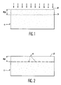
- la figure 1 représente, de façon schématique, une plaquette de matériau semiconducteur dont l'une de ses faces est soumise à un bombardement d'ions en application du procédé selon la présente invention,
- la figure 2 représente, de façon schématique, la plaquette précédente à l'issue de l'étape de traitement thermique destinée à faire coalescer les microcavités, selon la présente invention,
- la figure 3 représente, de façon schématique, la plaquette précédente après formation de composants électroniques dans la partie correspondant à la couche mince désirée,
- la figure 4 représente, de façon schématique, l'étape de séparation de la plaquette précédente en deux parties, conformément à la présente invention.
- FIG. 1 schematically represents a wafer of semiconductor material, one of its faces being subjected to ion bombardment by application of the method according to the present invention,
- FIG. 2 schematically represents the preceding wafer at the end of the heat treatment step intended to coalesce the microcavities, according to the present invention,
- FIG. 3 schematically represents the previous wafer after formation of electronic components in the part corresponding to the desired thin layer,
- Fig. 4 schematically shows the step of separating the previous wafer into two parts according to the present invention.
Un point important de la présente invention réside dans l'implantation d'ions d'hydrogène ou de gaz rare, selon une dose inférieure ou égale à la dose au-dessus de laquelle il y aurait séparation au cours du traitement thermique. La dose utilisée est telle qu'elle permet une fragilisation du matériau à une profondeur Rp correspondant au parcours moyen des ions dans le matériau, mais la plaquette reste suffisamment résistante mécaniquement pour supporter toutes les étapes de traitement thermique nécessaires à la réalisation de circuits électroniques. Autrement dit, la plaquette implantée présente, dans la zone de microcavités, des ponts solides reliant la partie de la plaquette destinée à constituer la couche mince à la partie restante de la plaquette.An important point of the present invention lies in the implantation of hydrogen or rare gas ions, in a dose less than or equal to the dose above which there would be separation during the heat treatment. The dose used is such that it allows embrittlement of the material at a depth Rp corresponding to the average path of the ions in the material, but the wafer remains mechanically strong enough to withstand all the heat treatment steps necessary for the production of electronic circuits. In other words, the implanted wafer has, in the microcavity zone, solid bridges connecting the portion of the wafer intended to constitute the thin layer to the remaining portion of the wafer.
La description va maintenant porter sur la réalisation d'une couche mince en matériau semiconducteur à partir d'un substrat épais présentant une face plane. Le substrat de départ peut être ou non recouvert sur cette face plane d'une ou de plusieurs couches de matériaux, comme par exemple des matériaux encapsulants tels qu'un diélectrique.The description will now relate to the production of a thin layer of semiconductor material from a thick substrate having a flat face. The starting substrate may or may not be covered on this plane face with one or more layers of materials, for example encapsulating materials such as a dielectric.
La figure 1 illustre l'étape d'implantation ionique d'une plaquette 1 en matériau semiconducteur. La face plane 2 de la plaquette reçoit le bombardement ionique qui est figuré par des flèches. Dans le cas où la face plane 2 de la plaquette est recouverte d'un ou de plusieurs matériaux non semiconducteurs, l'énergie des ions est choisie suffisante pour qu'ils pénètrent dans la masse de matériau semiconducteur.FIG. 1 illustrates the step of ion implantation of a
Le cas échéant, l'épaisseur de matériau semiconducteur implanté doit être telle que l'on puisse réaliser tout ou partie de composants électroniques et/ou des microstructures dans la couche mince. A titre d'exemple, la pénétration moyenne des ions hydrogène est de 2 µm à 200 keV dans du silicium.Where appropriate, the thickness of implanted semiconductor material must be such that all or part of the components can be and / or microstructures in the thin layer. For example, the average penetration of hydrogen ions is from 2 μm to 200 keV in silicon.
L'implantation ionique de ces types d'ions dans le substrat semiconducteur crée en profondeur, au voisinage de la profondeur correspondant au parcours moyen Rp des ions suivant une perpendiculaire à la face plane, une zone 3 à forte concentration en atomes donnant naissance à des microcavités. Par exemple, la concentration maximum en hydrogène est de 1021 H+/cm3 pour une dose d'implantation de 2.1016 H+/cm2 à 100 keV. Cette étape d'implantation ionique doit être réalisée à une température telle que les ions de gaz implantés ne diffusent pas au fur et à mesure (pendant l'étape d'implantation) à longue distance. Ceci perturberait ou annihilerait la formation de microcavités. Par exemple, dans le cas d'une implantation d'ions d'hydrogène dans du silicium on réalisera l'implantation ionique à une température inférieure à 350°C.The ion implantation of these types of ions in the semiconductor substrate creates, deep in the vicinity of the depth corresponding to the average path Rp of the ions along a perpendicular to the plane face, a
La dose d'implantation (nombre d'ions par unité de surface reçu pendant la durée de l'implantation) est choisie de sorte que la dose soit inférieure ou égale à une dose, dite dose critique, telle que, au-dessus de cette dose critique, pendant l'étape subséquente de traitement thermique, il y a séparation de la couche mince du reste de la plaquette. Dans le cas d'une implantation d'ions hydrogène, cette dose critique est de l'ordre de 4.1016 H+/cm2 pour une énergie de 160 keV.The implantation dose (number of ions per unit area received during the duration of the implantation) is chosen so that the dose is less than or equal to a dose, called the critical dose, such that, above this critical dose, during the subsequent heat treatment stage, there is separation of the thin layer from the rest of the wafer. In the case of implantation of hydrogen ions, this critical dose is of the order of 4.10 16 H + / cm 2 for an energy of 160 keV.
La dose d'implantation est également choisie supérieure à une dose minimum à partir de laquelle, lors de l'étape de traitement thermique subséquente, la formation de microcavités et l'interaction entre celles-ci est suffisante, c'est-à-dire qu'elle permet de fragiliser le matériau implanté dans la zone de microcavités 3. Cela veut dire qu'il existe encore des ponts solides de matériau semiconducteur situé entre les microcavités. Dans le cas d'une implantation d'ions de gaz hydrogène dans un substrat de silicium, cette dose minimum est de l'ordre de 1.1016/cm2 à une énergie de 100 keV.The implantation dose is also chosen greater than a minimum dose from which, during the subsequent heat treatment step, the formation of microcavities and the interaction between them is sufficient, that is to say it makes it possible to weaken the implanted material in the
L'étape suivante du procédé selon l'invention consiste en un traitement thermique de la plaquette à une température suffisante pour permettre une coalescence des microcavités suivant le plan de référence. Dans le cas d'une implantation, à une température inférieure à 350°C, d'ions de gaz hydrogène dans un substrat de silicium et une dose de 3.1016 H+/cm2 à une énergie de 100 keV, après un traitement thermique de trente minutes à 550°C, on observe par microscopie électronique à transmission en coupe, des cavités de hauteur égale à quelques fractions de nanomètres et d'extension suivant le plan de référence de plusieurs nanomètres voire plusieurs dizaines de nanomètres. Ce traitement thermique permet à la fois la précipitation et la stabilisation des atomes de gaz implantés sous forme de microcavités.The next step of the process according to the invention consists in a heat treatment of the wafer at a temperature sufficient to allow a coalescence of the microcavities according to the reference plane. In the case of an implantation, at a temperature below 350 ° C, hydrogen gas ions in a silicon substrate and a dose of 3.10 16 H + /
Les microcavités 4 (voir la figure 2) occupent, suivant le plan de référence, une surface sensiblement égale à la surface implantée. Les cavités 4 ne se situent pas exactement dans le même plan. Elles se trouvent dans des plans parallèles au plan de référence à quelques nanomètres ou dizaines de nanomètres de ce plan de référence. De ce fait, la partie supérieure du substrat situé entre le plan de référence et la face plane 2 n'est pas totalement séparée de la masse du substrat, la masse du substrat étant définie comme le reste du substrat compris entre le plan de référence et les faces du substrat autres que la face plane. Les liaisons restantes sont suffisamment fortes pour supporter des étapes de manipulation et de recuit dues aux étapes technologiques dans la réalisation de circuits intégrés. Cependant, la liaison entre la partie supérieure et la masse du substrat est très affaiblie puisque cette liaison n'est réalisée que par l'intermédiaire de ponts de matériau semiconducteur situés entre les cavités.Microcavities 4 (see Figure 2) occupy, according to the reference plane, a surface substantially equal to the implanted surface. The cavities 4 are not exactly in the same plane. They are in planes parallel to the reference plane a few nanometers or tens of nanometers from this reference plane. As a result, the upper part of the substrate situated between the reference plane and the
On peut ensuite réaliser sur la face plane 2 (à la surface et sous la surface) tout ou partie des composants électroniques, des circuits et des microstructures.It is then possible to produce on the flat face 2 (at the surface and under the surface) all or part of the electronic components, circuits and microstructures.
L'énergie d'implantation ionique des ions d'hydrogène ou de gaz rare de la première étape a été choisie de telle façon que la profondeur de la zone de microcavités soit suffisante pour qu'elle ne soit pas perturbée par la réalisation de composants, de circuits électroniques et/ou de microstructures durant cette étape. En outre, l'ensemble des opérations de recuit thermique que nécessite l'élaboration de composants, de circuits électroniques ou de microstructures, est choisi de façon à minimiser une éventuelle diffusion des ions implantés. Par exemple, dans le cas d'une plaquette de silicium monocristallin, on limitera préférentiellement la température maximum des diverses phases du procédé à 900°C.The ion implantation energy of the hydrogen or noble gas ions of the first stage has been chosen so that the depth of the microcavity zone is sufficient so that it is not disturbed by the production of components. electronic circuits and / or microstructures during this step. In addition, all the thermal annealing operations required for the development of components, electronic circuits or microstructures, is chosen so as to minimize possible diffusion of the implanted ions. For example, in the case of a monocrystalline silicon wafer, the maximum temperature of the various process phases will preferably be limited to 900 ° C.
La figure 3 illustre le cas où l'on a élaboré plusieurs composants électroniques, référencés 5, sur la face plane 2 et dans la partie de la plaquette destinée à constituer la couche mince.FIG. 3 illustrates the case where several electronic components, referenced 5, have been developed on the
L'étape de séparation vient ensuite. Elle consiste à appliquer des forces mécaniques, par exemple de traction, séparatrices entre les parties de la plaquette ou substrat situées de part et d'autre du plan de référence de façon à fracturer les ponts solides subsistants. Cette opération permet d'obtenir la couche mince de matériau semiconducteur, équipée de composants électroniques dans le cas décrit. La figure 4 illustre cette étape de séparation au cours de laquelle la couche mince 6 est séparée de la 'masse restante 7 du substrat par l'action de forces exerçant leurs actions en sens contraires et figurées par des flèches.The separation step comes next. It consists in applying mechanical forces, for example traction, separating between the parts of the wafer or substrate located on either side of the reference plane so as to fracture the remaining solid bridges. This operation makes it possible to obtain the thin layer of semiconductor material equipped with electronic components in the case described. FIG. 4 illustrates this separation step during which the
L'expérience montre que l'effort de traction nécessaire pour séparer la partie supérieure de la masse du substrat est faible en particulier lorsque l'on exerce un effort de cisaillement entre la partie supérieure et la masse du substrat, c'est-à-dire quand les forces exercées présentent une composante suivant le plan de référence. Ceci s'explique simplement par le fait que l'effort de cisaillement favorise la propagation des fractures et des cavités dans le plan de référence.Experience shows that the tensile force required to separate the upper part of the mass of the substrate is low, particularly when shearing force is exerted between the upper part and the mass of the substrate, that is to say say when the forces exerted have a component according to the reference plane. This is simply because the shear force promotes the propagation of fractures and cavities in the reference plane.
La partie supérieure du substrat étant par nature mince, l'effort de traction et/ou de cisaillement ne peut pas, dans bien des cas, être appliqué commodément directement sur celle-ci. Il est alors préférable, avant l'étape de séparation, de rendre la plaquette solidaire, par sa face plane 2, d'un support ou applicateur par l'intermédiaire duquel on appliquera les forces mécaniques à la partie supérieure de la plaquette. Cet applicateur est représenté sous la référence 8 à la figure 4.Since the upper part of the substrate is thin in nature, the tensile and / or shear force can not, in many cases, be conveniently applied directly to it. It is then preferable, before the separation step, to make the wafer integral, by its
L'applicateur peut être un support rigide ou souple. On entend ici par solidarisation de l'applicateur sur la plaquette toute opération de collage ou de préparation des surfaces et de mise en contact, permettant d'assurer une énergie de liaison suffisante entre l'applicateur et la face plane de la plaquette pour résister à l'opération de traction et/ou de cisaillement et/ou de flexion de l'étape de séparation.The applicator can be a rigid or flexible support. By the joining of the applicator on the wafer is meant any bonding operation or surface preparation and contacting, to ensure sufficient connection energy between the applicator and the flat face of the wafer to withstand the operation of traction and / or shearing and / or bending of the separation step.
L'applicateur peut être par exemple une feuille de matériau plastique tel que du Kapton® que l'on a rendu adhérent à la face plane du substrat. Dans cet exemple, après application du procédé selon l'invention, on obtient une couche mince de semiconducteur monocristallin sur feuille de Kapton®.The applicator may be for example a sheet of plastic material such as Kapton® that has been made adherent to the flat face of the substrate. In this example, after application of the process according to the invention, a monocrystalline semiconductor thin film is obtained on a Kapton® sheet.
Afin de transmettre correctement les efforts à l'ensemble de la couche mince supérieure, les circuits réalisés dans et à la surface de la couche supérieure peuvent avoir été recouverts d'une couche de protection éventuellement planarisante au cours de l'étape d'élaboration des composants électroniques. L'applicateur est alors solidarisé de la couche mince supérieure de la plaquette par l'intermédiaire de cette couche de protection.In order to correctly transmit the forces to the whole of the upper thin layer, the circuits made in and on the surface of the upper layer may have been covered with an optionally planar protective layer during the step of producing the electronic components. The applicator is then secured to the upper thin layer of the wafer through this protective layer.
L'applicateur peut être aussi un support rigide, par exemple une plaquette de silicium dont la surface peut être recouverte d'une couche diélectrique. On effectue par exemple un traitement physico-chimique approprié de la face plane de la plaquette et/ou de la surface de l'applicateur (portant ou non une couche diélectrique) pour que la mise en contact associée à un éventuel traitement thermique solidarise la face plane de la plaquette et l'applicateur.The applicator may also be a rigid support, for example a silicon wafer whose surface may be covered with a dielectric layer. For example, an appropriate physicochemical treatment of the flat face of the wafer and / or of the surface of the applicator (with or without a dielectric layer) is carried out so that the placing in contact associated with a possible heat treatment solidarises the face. plane of the wafer and the applicator.
Dans le cas cité à titre d'exemple où l'applicateur est une plaquette de silicium portant à sa surface une couche d'oxyde et où le substrat semiconducteur est une plaquette de silicium monocristallin, après application du procédé selon l'invention, on obtient une plaquette de silicium sur isolant où la couche de silicium superficielle est la couche fine fournie par la partie supérieure du substrat.In the case cited by way of example, where the applicator is a silicon wafer carrying on its surface an oxide layer and where the semiconductor substrate is a monocrystalline silicon wafer, after application of the method according to the invention, we obtain a silicon-on-insulator wafer where the superficial silicon layer is the thin layer provided by the upper part of the substrate.
En outre, après séparation de la couche mince du reste de la plaquette, la face libre de cette couche peut permettre le report d'un substrat supplémentaire pouvant être équipé de composants électroniques réalisés complètement ou partiellement sur le substrat. Un tel empilement permet un assemblage "trois dimensions" de circuits électroniques, le raidisseur pouvant ou non comporter lui-même des composants électroniques.In addition, after separation of the thin layer from the rest of the wafer, the free face of this layer can allow the transfer of an additional substrate that can be equipped with electronic components made completely or partially on the substrate. Such a stack allows a "three-dimensional" assembly of electronic circuits, the stiffener may or may not itself comprise electronic components.
Claims (19)
caractérisé en ce que :
characterized in that
Applications Claiming Priority (2)
| Application Number | Priority Date | Filing Date | Title |
|---|---|---|---|
| FR9606086A FR2748851B1 (en) | 1996-05-15 | 1996-05-15 | PROCESS FOR PRODUCING A THIN FILM OF SEMICONDUCTOR MATERIAL |
| EP97401062A EP0807970B1 (en) | 1996-05-15 | 1997-05-13 | Method of manufacturing a thin semiconductor layer |
Related Parent Applications (1)
| Application Number | Title | Priority Date | Filing Date |
|---|---|---|---|
| EP97401062A Division EP0807970B1 (en) | 1996-05-15 | 1997-05-13 | Method of manufacturing a thin semiconductor layer |
Publications (2)
| Publication Number | Publication Date |
|---|---|
| EP1768176A2 true EP1768176A2 (en) | 2007-03-28 |
| EP1768176A3 EP1768176A3 (en) | 2007-04-04 |
Family
ID=9492177
Family Applications (2)
| Application Number | Title | Priority Date | Filing Date |
|---|---|---|---|
| EP06291790A Withdrawn EP1768176A3 (en) | 1996-05-15 | 1997-05-13 | Method of manufacturing a thin semiconductor layer |
| EP97401062A Revoked EP0807970B1 (en) | 1996-05-15 | 1997-05-13 | Method of manufacturing a thin semiconductor layer |
Family Applications After (1)
| Application Number | Title | Priority Date | Filing Date |
|---|---|---|---|
| EP97401062A Revoked EP0807970B1 (en) | 1996-05-15 | 1997-05-13 | Method of manufacturing a thin semiconductor layer |
Country Status (9)
| Country | Link |
|---|---|
| US (7) | US6020252A (en) |
| EP (2) | EP1768176A3 (en) |
| JP (2) | JP3517080B2 (en) |
| KR (1) | KR100704107B1 (en) |
| DE (1) | DE69738608T2 (en) |
| FR (1) | FR2748851B1 (en) |
| MY (1) | MY125679A (en) |
| SG (1) | SG52966A1 (en) |
| TW (1) | TW366527B (en) |
Families Citing this family (429)
| Publication number | Priority date | Publication date | Assignee | Title |
|---|---|---|---|---|
| TW374196B (en) | 1996-02-23 | 1999-11-11 | Semiconductor Energy Lab Co Ltd | Semiconductor thin film and method for manufacturing the same and semiconductor device and method for manufacturing the same |
| FR2748851B1 (en) | 1996-05-15 | 1998-08-07 | Commissariat Energie Atomique | PROCESS FOR PRODUCING A THIN FILM OF SEMICONDUCTOR MATERIAL |
| US20050280155A1 (en) * | 2004-06-21 | 2005-12-22 | Sang-Yun Lee | Semiconductor bonding and layer transfer method |
| US7052941B2 (en) * | 2003-06-24 | 2006-05-30 | Sang-Yun Lee | Method for making a three-dimensional integrated circuit structure |
| US8018058B2 (en) * | 2004-06-21 | 2011-09-13 | Besang Inc. | Semiconductor memory device |
| US8058142B2 (en) * | 1996-11-04 | 2011-11-15 | Besang Inc. | Bonded semiconductor structure and method of making the same |
| FR2755537B1 (en) * | 1996-11-05 | 1999-03-05 | Commissariat Energie Atomique | METHOD FOR MANUFACTURING A THIN FILM ON A SUPPORT AND STRUCTURE THUS OBTAINED |
| SG71094A1 (en) * | 1997-03-26 | 2000-03-21 | Canon Kk | Thin film formation using laser beam heating to separate layers |
| US6162705A (en) | 1997-05-12 | 2000-12-19 | Silicon Genesis Corporation | Controlled cleavage process and resulting device using beta annealing |
| US20070122997A1 (en) | 1998-02-19 | 2007-05-31 | Silicon Genesis Corporation | Controlled process and resulting device |
| US6033974A (en) | 1997-05-12 | 2000-03-07 | Silicon Genesis Corporation | Method for controlled cleaving process |
| US6582999B2 (en) | 1997-05-12 | 2003-06-24 | Silicon Genesis Corporation | Controlled cleavage process using pressurized fluid |
| EP0889505B1 (en) * | 1997-07-03 | 2005-06-08 | STMicroelectronics S.r.l. | Process for cutting trenches in a single crystal substrate |
| US6548382B1 (en) | 1997-07-18 | 2003-04-15 | Silicon Genesis Corporation | Gettering technique for wafers made using a controlled cleaving process |
| US6534380B1 (en) * | 1997-07-18 | 2003-03-18 | Denso Corporation | Semiconductor substrate and method of manufacturing the same |
| US6686623B2 (en) | 1997-11-18 | 2004-02-03 | Semiconductor Energy Laboratory Co., Ltd. | Nonvolatile memory and electronic apparatus |
| FR2773261B1 (en) | 1997-12-30 | 2000-01-28 | Commissariat Energie Atomique | METHOD FOR THE TRANSFER OF A THIN FILM COMPRISING A STEP OF CREATING INCLUSIONS |
| MY118019A (en) * | 1998-02-18 | 2004-08-30 | Canon Kk | Composite member, its separation method, and preparation method of semiconductor substrate by utilization thereof |
| US7227176B2 (en) | 1998-04-10 | 2007-06-05 | Massachusetts Institute Of Technology | Etch stop layer system |
| JP2000012864A (en) * | 1998-06-22 | 2000-01-14 | Semiconductor Energy Lab Co Ltd | Manufacture of semiconductor device |
| US6054370A (en) * | 1998-06-30 | 2000-04-25 | Intel Corporation | Method of delaminating a pre-fabricated transistor layer from a substrate for placement on another wafer |
| JP3395661B2 (en) * | 1998-07-07 | 2003-04-14 | 信越半導体株式会社 | Method for manufacturing SOI wafer |
| US6271101B1 (en) | 1998-07-29 | 2001-08-07 | Semiconductor Energy Laboratory Co., Ltd. | Process for production of SOI substrate and process for production of semiconductor device |
| DE19837944A1 (en) * | 1998-08-21 | 2000-02-24 | Asea Brown Boveri | Method of manufacturing a semiconductor device |
| JP4476390B2 (en) | 1998-09-04 | 2010-06-09 | 株式会社半導体エネルギー研究所 | Method for manufacturing semiconductor device |
| FR2784795B1 (en) * | 1998-10-16 | 2000-12-01 | Commissariat Energie Atomique | STRUCTURE COMPRISING A THIN LAYER OF MATERIAL COMPOSED OF CONDUCTIVE ZONES AND INSULATING ZONES AND METHOD FOR MANUFACTURING SUCH A STRUCTURE |
| FR2784794A1 (en) * | 1998-10-20 | 2000-04-21 | Commissariat Energie Atomique | Electronic structure, especially an IC chip, has an insulating support formed by particle irradiation of a semiconductor wafer |
| US6555443B1 (en) * | 1998-11-11 | 2003-04-29 | Robert Bosch Gmbh | Method for production of a thin film and a thin-film solar cell, in particular, on a carrier substrate |
| DE19936941B4 (en) * | 1998-11-11 | 2008-11-06 | Robert Bosch Gmbh | Method for producing thin layers, in particular thin-film solar cells, on a carrier substrate |
| US20050124142A1 (en) * | 1998-12-31 | 2005-06-09 | Bower Robert W. | Transposed split of ion cut materials |
| US6534381B2 (en) * | 1999-01-08 | 2003-03-18 | Silicon Genesis Corporation | Method for fabricating multi-layered substrates |
| US6355541B1 (en) * | 1999-04-21 | 2002-03-12 | Lockheed Martin Energy Research Corporation | Method for transfer of thin-film of silicon carbide via implantation and wafer bonding |
| JP2001015721A (en) * | 1999-04-30 | 2001-01-19 | Canon Inc | Separation method of composite member and manufacture of thin film |
| US6162702A (en) * | 1999-06-17 | 2000-12-19 | Intersil Corporation | Self-supported ultra thin silicon wafer process |
| FR2795866B1 (en) | 1999-06-30 | 2001-08-17 | Commissariat Energie Atomique | METHOD FOR PRODUCING A THIN MEMBRANE AND MEMBRANE STRUCTURE THUS OBTAINED |
| FR2797347B1 (en) * | 1999-08-04 | 2001-11-23 | Commissariat Energie Atomique | METHOD FOR TRANSFERRING A THIN FILM HAVING A SURFRAGILILIZATION STEP |
| US6500732B1 (en) | 1999-08-10 | 2002-12-31 | Silicon Genesis Corporation | Cleaving process to fabricate multilayered substrates using low implantation doses |
| JP2003506883A (en) * | 1999-08-10 | 2003-02-18 | シリコン ジェネシス コーポレイション | Cleavage process for manufacturing multi-layer substrates with low implant dose |
| US6263941B1 (en) | 1999-08-10 | 2001-07-24 | Silicon Genesis Corporation | Nozzle for cleaving substrates |
| FR2797713B1 (en) | 1999-08-20 | 2002-08-02 | Soitec Silicon On Insulator | PROCESS FOR PROCESSING SUBSTRATES FOR MICROELECTRONICS AND SUBSTRATES OBTAINED BY THIS PROCESS |
| FR2802340B1 (en) * | 1999-12-13 | 2003-09-05 | Commissariat Energie Atomique | STRUCTURE COMPRISING PHOTOVOLTAIC CELLS AND METHOD FOR PRODUCING THE SAME |
| US7427526B2 (en) * | 1999-12-20 | 2008-09-23 | The Penn State Research Foundation | Deposited thin films and their use in separation and sacrificial layer applications |
| JP2001189288A (en) * | 1999-12-20 | 2001-07-10 | Ind Technol Res Inst | Board-dicing method using ion implantation |
| US6544862B1 (en) | 2000-01-14 | 2003-04-08 | Silicon Genesis Corporation | Particle distribution method and resulting structure for a layer transfer process |
| TW452866B (en) * | 2000-02-25 | 2001-09-01 | Lee Tien Hsi | Manufacturing method of thin film on a substrate |
| JP2003531492A (en) * | 2000-04-14 | 2003-10-21 | エス オー イ テク シリコン オン インシュレータ テクノロジース | Method of cutting at least one thin layer from a substrate or ingot, especially made of semiconductor material |
| US6709955B2 (en) * | 2000-04-17 | 2004-03-23 | Stmicroelectronics S.R.L. | Method of fabricating electronic devices integrated in semiconductor substrates provided with gettering sites, and a device fabricated by the method |
| FR2809867B1 (en) * | 2000-05-30 | 2003-10-24 | Commissariat Energie Atomique | FRAGILE SUBSTRATE AND METHOD FOR MANUFACTURING SUCH SUBSTRATE |
| JP3580227B2 (en) * | 2000-06-21 | 2004-10-20 | 三菱住友シリコン株式会社 | Composite substrate separation method and separation device |
| FR2811807B1 (en) * | 2000-07-12 | 2003-07-04 | Commissariat Energie Atomique | METHOD OF CUTTING A BLOCK OF MATERIAL AND FORMING A THIN FILM |
| JP5066321B2 (en) | 2000-08-04 | 2012-11-07 | 台湾積體電路製造股▲ふん▼有限公司 | Silicon wafer with embedded optoelectronic material for monolithic OEIC |
| JP2004507084A (en) * | 2000-08-16 | 2004-03-04 | マサチューセッツ インスティテュート オブ テクノロジー | Manufacturing process of semiconductor products using graded epitaxial growth |
| FR2816445B1 (en) * | 2000-11-06 | 2003-07-25 | Commissariat Energie Atomique | METHOD FOR MANUFACTURING A STACKED STRUCTURE COMPRISING A THIN LAYER ADHERING TO A TARGET SUBSTRATE |
| FR2840731B3 (en) * | 2002-06-11 | 2004-07-30 | Soitec Silicon On Insulator | METHOD FOR MANUFACTURING A SUBSTRATE HAVING A USEFUL LAYER OF SINGLE-CRYSTAL SEMICONDUCTOR MATERIAL OF IMPROVED PROPERTIES |
| US8507361B2 (en) | 2000-11-27 | 2013-08-13 | Soitec | Fabrication of substrates with a useful layer of monocrystalline semiconductor material |
| FR2894990B1 (en) * | 2005-12-21 | 2008-02-22 | Soitec Silicon On Insulator | PROCESS FOR PRODUCING SUBSTRATES, IN PARTICULAR FOR OPTICS, ELECTRONICS OR OPTOELECTRONICS AND SUBSTRATE OBTAINED BY SAID PROCESS |
| JP3957038B2 (en) * | 2000-11-28 | 2007-08-08 | シャープ株式会社 | Semiconductor substrate and manufacturing method thereof |
| US7094667B1 (en) | 2000-12-28 | 2006-08-22 | Bower Robert W | Smooth thin film layers produced by low temperature hydrogen ion cut |
| FR2821697B1 (en) * | 2001-03-02 | 2004-06-25 | Commissariat Energie Atomique | METHOD OF MANUFACTURING THIN LAYERS ON A SPECIFIC CARRIER AND AN APPLICATION |
| JP4749584B2 (en) * | 2001-03-30 | 2011-08-17 | 株式会社豊田中央研究所 | Manufacturing method of semiconductor substrate |
| WO2002082514A1 (en) * | 2001-04-04 | 2002-10-17 | Massachusetts Institute Of Technology | A method for semiconductor device fabrication |
| FR2823596B1 (en) * | 2001-04-13 | 2004-08-20 | Commissariat Energie Atomique | SUBSTRATE OR DISMOUNTABLE STRUCTURE AND METHOD OF MAKING SAME |
| FR2823599B1 (en) | 2001-04-13 | 2004-12-17 | Commissariat Energie Atomique | DEMOMTABLE SUBSTRATE WITH CONTROLLED MECHANICAL HOLDING AND METHOD OF MAKING |
| US20050026432A1 (en) * | 2001-04-17 | 2005-02-03 | Atwater Harry A. | Wafer bonded epitaxial templates for silicon heterostructures |
| WO2002084725A1 (en) | 2001-04-17 | 2002-10-24 | California Institute Of Technology | A method of using a germanium layer transfer to si for photovoltaic applications and heterostructure made thereby |
| US7238622B2 (en) * | 2001-04-17 | 2007-07-03 | California Institute Of Technology | Wafer bonded virtual substrate and method for forming the same |
| US7045878B2 (en) * | 2001-05-18 | 2006-05-16 | Reveo, Inc. | Selectively bonded thin film layer and substrate layer for processing of useful devices |
| US6956268B2 (en) * | 2001-05-18 | 2005-10-18 | Reveo, Inc. | MEMS and method of manufacturing MEMS |
| DE10131249A1 (en) * | 2001-06-28 | 2002-05-23 | Wacker Siltronic Halbleitermat | Production of a film or a layer of semiconductor material comprises producing structures of repeating recesses on the surface of a semiconductor material |
| JP4102040B2 (en) * | 2001-07-31 | 2008-06-18 | 信越半導体株式会社 | SOI wafer manufacturing method and wafer separation jig |
| FR2828762B1 (en) * | 2001-08-14 | 2003-12-05 | Soitec Silicon On Insulator | METHOD FOR OBTAINING A THIN FILM OF A SEMICONDUCTOR MATERIAL SUPPORTING AT LEAST ONE ELECTRONIC COMPONENT AND / OR CIRCUIT |
| US7033910B2 (en) * | 2001-09-12 | 2006-04-25 | Reveo, Inc. | Method of fabricating multi layer MEMS and microfluidic devices |
| US7163826B2 (en) | 2001-09-12 | 2007-01-16 | Reveo, Inc | Method of fabricating multi layer devices on buried oxide layer substrates |
| US6875671B2 (en) * | 2001-09-12 | 2005-04-05 | Reveo, Inc. | Method of fabricating vertical integrated circuits |
| US20090065471A1 (en) * | 2003-02-10 | 2009-03-12 | Faris Sadeg M | Micro-nozzle, nano-nozzle, manufacturing methods therefor, applications therefor |
| US6555451B1 (en) | 2001-09-28 | 2003-04-29 | The United States Of America As Represented By The Secretary Of The Navy | Method for making shallow diffusion junctions in semiconductors using elemental doping |
| FR2830983B1 (en) | 2001-10-11 | 2004-05-14 | Commissariat Energie Atomique | METHOD FOR MANUFACTURING THIN FILMS CONTAINING MICROCOMPONENTS |
| US6593212B1 (en) | 2001-10-29 | 2003-07-15 | The United States Of America As Represented By The Secretary Of The Navy | Method for making electro-optical devices using a hydrogenion splitting technique |
| US7309620B2 (en) * | 2002-01-11 | 2007-12-18 | The Penn State Research Foundation | Use of sacrificial layers in the manufacture of high performance systems on tailored substrates |
| US6562127B1 (en) | 2002-01-16 | 2003-05-13 | The United States Of America As Represented By The Secretary Of The Navy | Method of making mosaic array of thin semiconductor material of large substrates |
| FR2835097B1 (en) * | 2002-01-23 | 2005-10-14 | OPTIMIZED METHOD FOR DEFERRING A THIN LAYER OF SILICON CARBIDE ON A RECEPTACLE SUBSTRATE | |
| US7060632B2 (en) * | 2002-03-14 | 2006-06-13 | Amberwave Systems Corporation | Methods for fabricating strained layers on semiconductor substrates |
| US6607969B1 (en) | 2002-03-18 | 2003-08-19 | The United States Of America As Represented By The Secretary Of The Navy | Method for making pyroelectric, electro-optical and decoupling capacitors using thin film transfer and hydrogen ion splitting techniques |
| FR2837981B1 (en) * | 2002-03-28 | 2005-01-07 | Commissariat Energie Atomique | PROCESS FOR HANDLING SEMICONDUCTOR LAYERS FOR THEIR SLOWDOWN |
| US6767749B2 (en) | 2002-04-22 | 2004-07-27 | The United States Of America As Represented By The Secretary Of The Navy | Method for making piezoelectric resonator and surface acoustic wave device using hydrogen implant layer splitting |
| JP4277481B2 (en) * | 2002-05-08 | 2009-06-10 | 日本電気株式会社 | Semiconductor substrate manufacturing method and semiconductor device manufacturing method |
| US7459025B2 (en) * | 2002-06-03 | 2008-12-02 | Tien-Hsi Lee | Methods for transferring a layer onto a substrate |
| US6995430B2 (en) * | 2002-06-07 | 2006-02-07 | Amberwave Systems Corporation | Strained-semiconductor-on-insulator device structures |
| US7335545B2 (en) * | 2002-06-07 | 2008-02-26 | Amberwave Systems Corporation | Control of strain in device layers by prevention of relaxation |
| US7074623B2 (en) * | 2002-06-07 | 2006-07-11 | Amberwave Systems Corporation | Methods of forming strained-semiconductor-on-insulator finFET device structures |
| US20030227057A1 (en) * | 2002-06-07 | 2003-12-11 | Lochtefeld Anthony J. | Strained-semiconductor-on-insulator device structures |
| US7307273B2 (en) * | 2002-06-07 | 2007-12-11 | Amberwave Systems Corporation | Control of strain in device layers by selective relaxation |
| FR2842650B1 (en) * | 2002-07-17 | 2005-09-02 | Soitec Silicon On Insulator | PROCESS FOR PRODUCING SUBSTRATES, IN PARTICULAR FOR OPTICS, ELECTRONICS OR OPTO-ELECTRONICS |
| US6979630B2 (en) * | 2002-08-08 | 2005-12-27 | Isonics Corporation | Method and apparatus for transferring a thin layer of semiconductor material |
| US8187377B2 (en) * | 2002-10-04 | 2012-05-29 | Silicon Genesis Corporation | Non-contact etch annealing of strained layers |
| GB2409340B (en) | 2002-10-04 | 2006-05-10 | Silicon Genesis Corp | Method for treating semiconductor material |
| FR2845518B1 (en) | 2002-10-07 | 2005-10-14 | Commissariat Energie Atomique | IMPLEMENTING A DEMONDABLE SEMICONDUCTOR SUBSTRATE AND OBTAINING A SEMICONDUCTOR ELEMENT |
| FR2845517B1 (en) * | 2002-10-07 | 2005-05-06 | Commissariat Energie Atomique | IMPLEMENTING A DEMONDABLE SEMICONDUCTOR SUBSTRATE AND OBTAINING A SEMICONDUCTOR ELEMENT |
| JP4556158B2 (en) * | 2002-10-22 | 2010-10-06 | 株式会社Sumco | Method for manufacturing bonded SOI substrate and semiconductor device |
| FR2847075B1 (en) * | 2002-11-07 | 2005-02-18 | Commissariat Energie Atomique | PROCESS FOR FORMING A FRAGILE ZONE IN A SUBSTRATE BY CO-IMPLANTATION |
| US7176108B2 (en) | 2002-11-07 | 2007-02-13 | Soitec Silicon On Insulator | Method of detaching a thin film at moderate temperature after co-implantation |
| US7056815B1 (en) * | 2002-11-12 | 2006-06-06 | The Regents Of The University Of Michigan | Narrow energy band gap gallium arsenide nitride semi-conductors and an ion-cut-synthesis method for producing the same |
| FR2848336B1 (en) * | 2002-12-09 | 2005-10-28 | Commissariat Energie Atomique | METHOD FOR PRODUCING A STRESS STRUCTURE FOR DISSOCIATING |
| US20100133695A1 (en) * | 2003-01-12 | 2010-06-03 | Sang-Yun Lee | Electronic circuit with embedded memory |
| FR2850390B1 (en) * | 2003-01-24 | 2006-07-14 | Soitec Silicon On Insulator | METHOD FOR REMOVING A PERIPHERAL GLUE ZONE WHEN MANUFACTURING A COMPOSITE SUBSTRATE |
| US7122095B2 (en) * | 2003-03-14 | 2006-10-17 | S.O.I.Tec Silicon On Insulator Technologies S.A. | Methods for forming an assembly for transfer of a useful layer |
| JP4509488B2 (en) | 2003-04-02 | 2010-07-21 | 株式会社Sumco | Manufacturing method of bonded substrate |
| EP1482548B1 (en) | 2003-05-26 | 2016-04-13 | Soitec | A method of manufacturing a wafer |
| US8071438B2 (en) * | 2003-06-24 | 2011-12-06 | Besang Inc. | Semiconductor circuit |
| FR2856844B1 (en) | 2003-06-24 | 2006-02-17 | Commissariat Energie Atomique | HIGH PERFORMANCE CHIP INTEGRATED CIRCUIT |
| FR2857953B1 (en) | 2003-07-21 | 2006-01-13 | Commissariat Energie Atomique | STACKED STRUCTURE, AND METHOD FOR MANUFACTURING THE SAME |
| FR2859312B1 (en) * | 2003-09-02 | 2006-02-17 | Soitec Silicon On Insulator | MULTIFUNCTIONAL METAL SEAL |
| US8475693B2 (en) * | 2003-09-30 | 2013-07-02 | Soitec | Methods of making substrate structures having a weakened intermediate layer |
| FR2861497B1 (en) * | 2003-10-28 | 2006-02-10 | Soitec Silicon On Insulator | METHOD FOR CATASTROPHIC TRANSFER OF A FINE LAYER AFTER CO-IMPLANTATION |
| US7354815B2 (en) * | 2003-11-18 | 2008-04-08 | Silicon Genesis Corporation | Method for fabricating semiconductor devices using strained silicon bearing material |
| US7772087B2 (en) | 2003-12-19 | 2010-08-10 | Commissariat A L'energie Atomique | Method of catastrophic transfer of a thin film after co-implantation |
| US6992025B2 (en) * | 2004-01-12 | 2006-01-31 | Sharp Laboratories Of America, Inc. | Strained silicon on insulator from film transfer and relaxation by hydrogen implantation |
| EP1569263B1 (en) * | 2004-02-27 | 2011-11-23 | OSRAM Opto Semiconductors GmbH | Method for joining two wafers |
| US7390724B2 (en) | 2004-04-12 | 2008-06-24 | Silicon Genesis Corporation | Method and system for lattice space engineering |
| US20080211061A1 (en) * | 2004-04-21 | 2008-09-04 | California Institute Of Technology | Method For the Fabrication of GaAs/Si and Related Wafer Bonded Virtual Substrates |
| EP2293326A3 (en) * | 2004-06-10 | 2012-01-25 | S.O.I.TEC Silicon on Insulator Technologies S.A. | Method for manufacturing a SOI wafer |
| DE102004030612B3 (en) | 2004-06-24 | 2006-04-20 | Siltronic Ag | Semiconductor substrate and method for its production |
| US7094666B2 (en) * | 2004-07-29 | 2006-08-22 | Silicon Genesis Corporation | Method and system for fabricating strained layers for the manufacture of integrated circuits |
| US20060021565A1 (en) * | 2004-07-30 | 2006-02-02 | Aonex Technologies, Inc. | GaInP / GaAs / Si triple junction solar cell enabled by wafer bonding and layer transfer |
| US7439152B2 (en) * | 2004-08-27 | 2008-10-21 | Micron Technology, Inc. | Methods of forming a plurality of capacitors |
| US7202124B2 (en) * | 2004-10-01 | 2007-04-10 | Massachusetts Institute Of Technology | Strained gettering layers for semiconductor processes |
| US7846759B2 (en) * | 2004-10-21 | 2010-12-07 | Aonex Technologies, Inc. | Multi-junction solar cells and methods of making same using layer transfer and bonding techniques |
| DE102004054564B4 (en) * | 2004-11-11 | 2008-11-27 | Siltronic Ag | Semiconductor substrate and method for its production |
| US20060113603A1 (en) * | 2004-12-01 | 2006-06-01 | Amberwave Systems Corporation | Hybrid semiconductor-on-insulator structures and related methods |
| US7393733B2 (en) * | 2004-12-01 | 2008-07-01 | Amberwave Systems Corporation | Methods of forming hybrid fin field-effect transistor structures |
| US7344957B2 (en) * | 2005-01-19 | 2008-03-18 | Texas Instruments Incorporated | SOI wafer with cooling channels and a method of manufacture thereof |
| US10374120B2 (en) * | 2005-02-18 | 2019-08-06 | Koninklijke Philips N.V. | High efficiency solar cells utilizing wafer bonding and layer transfer to integrate non-lattice matched materials |
| US20110143506A1 (en) * | 2009-12-10 | 2011-06-16 | Sang-Yun Lee | Method for fabricating a semiconductor memory device |
| US8367524B2 (en) * | 2005-03-29 | 2013-02-05 | Sang-Yun Lee | Three-dimensional integrated circuit structure |
| WO2006103491A1 (en) * | 2005-03-29 | 2006-10-05 | S.O.I.Tec Silicon On Insulator Technologies | Hybrid fully soi-type multilayer structure |
| US8101498B2 (en) * | 2005-04-21 | 2012-01-24 | Pinnington Thomas Henry | Bonded intermediate substrate and method of making same |
| US20060240275A1 (en) * | 2005-04-25 | 2006-10-26 | Gadkaree Kishor P | Flexible display substrates |
| US7897443B2 (en) * | 2005-04-26 | 2011-03-01 | Sharp Kabushiki Kaisha | Production method of semiconductor device and semiconductor device |
| FR2886051B1 (en) | 2005-05-20 | 2007-08-10 | Commissariat Energie Atomique | METHOD FOR DETACHING THIN FILM |
| US7674687B2 (en) * | 2005-07-27 | 2010-03-09 | Silicon Genesis Corporation | Method and structure for fabricating multiple tiled regions onto a plate using a controlled cleaving process |
| FR2889887B1 (en) | 2005-08-16 | 2007-11-09 | Commissariat Energie Atomique | METHOD FOR DEFERING A THIN LAYER ON A SUPPORT |
| FR2891281B1 (en) | 2005-09-28 | 2007-12-28 | Commissariat Energie Atomique | METHOD FOR MANUFACTURING A THIN FILM ELEMENT |
| JP5064695B2 (en) * | 2006-02-16 | 2012-10-31 | 信越化学工業株式会社 | Manufacturing method of SOI substrate |
| FR2898431B1 (en) * | 2006-03-13 | 2008-07-25 | Soitec Silicon On Insulator | METHOD FOR MANUFACTURING THIN FILM |
| FR2899378B1 (en) | 2006-03-29 | 2008-06-27 | Commissariat Energie Atomique | METHOD FOR DETACHING A THIN FILM BY FUSION OF PRECIPITS |
| US20070243703A1 (en) * | 2006-04-14 | 2007-10-18 | Aonex Technololgies, Inc. | Processes and structures for epitaxial growth on laminate substrates |
| FR2914110B1 (en) | 2007-03-20 | 2009-06-05 | Soitec Silicon On Insulator | PROCESS FOR PRODUCING A HYBRID SUBSTRATE |
| US8293619B2 (en) | 2008-08-28 | 2012-10-23 | Silicon Genesis Corporation | Layer transfer of films utilizing controlled propagation |
| US9362439B2 (en) | 2008-05-07 | 2016-06-07 | Silicon Genesis Corporation | Layer transfer of films utilizing controlled shear region |
| US7811900B2 (en) | 2006-09-08 | 2010-10-12 | Silicon Genesis Corporation | Method and structure for fabricating solar cells using a thick layer transfer process |
| US8993410B2 (en) | 2006-09-08 | 2015-03-31 | Silicon Genesis Corporation | Substrate cleaving under controlled stress conditions |
| WO2008058252A2 (en) * | 2006-11-08 | 2008-05-15 | Silicon China (Hk) Limited | System and method for a photovoltaic structure |
| JP2008153411A (en) * | 2006-12-18 | 2008-07-03 | Shin Etsu Chem Co Ltd | Manufacturing method of soi substrate |
| FR2910179B1 (en) | 2006-12-19 | 2009-03-13 | Commissariat Energie Atomique | METHOD FOR MANUFACTURING THIN LAYERS OF GaN BY IMPLANTATION AND RECYCLING OF A STARTING SUBSTRATE |
| FR2910702B1 (en) * | 2006-12-26 | 2009-04-03 | Soitec Silicon On Insulator | METHOD FOR MANUFACTURING A MIXED SUBSTRATE |
| WO2008123116A1 (en) * | 2007-03-26 | 2008-10-16 | Semiconductor Energy Laboratory Co., Ltd. | Soi substrate and method for manufacturing soi substrate |
| WO2008123117A1 (en) * | 2007-03-26 | 2008-10-16 | Semiconductor Energy Laboratory Co., Ltd. | Soi substrate and method for manufacturing soi substrate |
| CN101657882B (en) | 2007-04-13 | 2012-05-30 | 株式会社半导体能源研究所 | Display device, method for manufacturing display device, and SOI substrate |
| KR101447048B1 (en) | 2007-04-20 | 2014-10-06 | 가부시키가이샤 한도오따이 에네루기 켄큐쇼 | Method for manufacturing soi substrate and semiconductor device |
| US7732301B1 (en) | 2007-04-20 | 2010-06-08 | Pinnington Thomas Henry | Bonded intermediate substrate and method of making same |
| US7867805B2 (en) * | 2007-05-13 | 2011-01-11 | International Business Machines Corporation | Structure replication through ultra thin layer transfer |
| US9059247B2 (en) * | 2007-05-18 | 2015-06-16 | Semiconductor Energy Laboratory Co., Ltd. | Method for manufacturing SOI substrate and method for manufacturing semiconductor device |
| TWI335046B (en) * | 2007-05-25 | 2010-12-21 | Univ Nat Taiwan | Flexible electronic device and process for the same |
| US20090278233A1 (en) * | 2007-07-26 | 2009-11-12 | Pinnington Thomas Henry | Bonded intermediate substrate and method of making same |
| JP5367330B2 (en) * | 2007-09-14 | 2013-12-11 | 株式会社半導体エネルギー研究所 | Method for manufacturing SOI substrate and method for manufacturing semiconductor device |
| US8236668B2 (en) * | 2007-10-10 | 2012-08-07 | Semiconductor Energy Laboratory Co., Ltd. | Method for manufacturing SOI substrate |
| FR2922359B1 (en) * | 2007-10-12 | 2009-12-18 | Commissariat Energie Atomique | METHOD FOR MANUFACTURING A MICROELECTRONIC STRUCTURE INVOLVING MOLECULAR COLLAGE |
| FR2922681A1 (en) * | 2007-10-23 | 2009-04-24 | Soitec Silicon On Insulator | METHOD FOR DETACHING A SUBSTRATE |
| JP5548351B2 (en) * | 2007-11-01 | 2014-07-16 | 株式会社半導体エネルギー研究所 | Method for manufacturing semiconductor device |
| US20090124038A1 (en) * | 2007-11-14 | 2009-05-14 | Mark Ewing Tuttle | Imager device, camera, and method of manufacturing a back side illuminated imager |
| JP5464843B2 (en) | 2007-12-03 | 2014-04-09 | 株式会社半導体エネルギー研究所 | Method for manufacturing SOI substrate |
| FR2925221B1 (en) | 2007-12-17 | 2010-02-19 | Commissariat Energie Atomique | METHOD FOR TRANSFERRING A THIN LAYER |
| US20090159111A1 (en) * | 2007-12-21 | 2009-06-25 | The Woodside Group Pte. Ltd | Photovoltaic device having a textured metal silicide layer |
| US20090162966A1 (en) * | 2007-12-21 | 2009-06-25 | The Woodside Group Pte Ltd | Structure and method of formation of a solar cell |
| US8129613B2 (en) * | 2008-02-05 | 2012-03-06 | Twin Creeks Technologies, Inc. | Photovoltaic cell comprising a thin lamina having low base resistivity and method of making |
| US8481845B2 (en) * | 2008-02-05 | 2013-07-09 | Gtat Corporation | Method to form a photovoltaic cell comprising a thin lamina |
| US8563352B2 (en) * | 2008-02-05 | 2013-10-22 | Gtat Corporation | Creation and translation of low-relief texture for a photovoltaic cell |
| US20090212397A1 (en) * | 2008-02-22 | 2009-08-27 | Mark Ewing Tuttle | Ultrathin integrated circuit and method of manufacturing an ultrathin integrated circuit |
| FR2930072B1 (en) * | 2008-04-15 | 2010-08-20 | Commissariat Energie Atomique | METHOD OF TRANSFERRING A THIN LAYER BY PROTONIC EXCHANGE |
| US7749884B2 (en) * | 2008-05-06 | 2010-07-06 | Astrowatt, Inc. | Method of forming an electronic device using a separation-enhancing species |
| WO2009143026A2 (en) * | 2008-05-17 | 2009-11-26 | Astrowatt, Inc. | Method of forming an electronic device using a separation technique |
| EP2281302B1 (en) | 2008-05-21 | 2012-12-26 | Nxp B.V. | A method of manufacturing a bipolar transistor semiconductor device |
| US8501522B2 (en) | 2008-05-30 | 2013-08-06 | Gtat Corporation | Intermetal stack for use in a photovoltaic cell |
| US8049104B2 (en) * | 2009-09-30 | 2011-11-01 | Twin Creek Technologies, Inc. | Intermetal stack for use in a photovoltaic cell |
| US8207590B2 (en) * | 2008-07-03 | 2012-06-26 | Samsung Electronics Co., Ltd. | Image sensor, substrate for the same, image sensing device including the image sensor, and associated methods |
| US7902091B2 (en) * | 2008-08-13 | 2011-03-08 | Varian Semiconductor Equipment Associates, Inc. | Cleaving of substrates |
| US8330126B2 (en) | 2008-08-25 | 2012-12-11 | Silicon Genesis Corporation | Race track configuration and method for wafering silicon solar substrates |
| US8765508B2 (en) * | 2008-08-27 | 2014-07-01 | Soitec | Methods of fabricating semiconductor structures or devices using layers of semiconductor material having selected or controlled lattice parameters |
| US8815618B2 (en) | 2008-08-29 | 2014-08-26 | Tsmc Solid State Lighting Ltd. | Light-emitting diode on a conductive substrate |
| FR2935535B1 (en) * | 2008-09-02 | 2010-12-10 | S O I Tec Silicon On Insulator Tech | METHOD FOR JOINT DETOURING. |
| US8486771B2 (en) * | 2008-09-24 | 2013-07-16 | Soitec | Methods of forming relaxed layers of semiconductor materials, semiconductor structures, devices and engineered substrates including same |
| US8637383B2 (en) | 2010-12-23 | 2014-01-28 | Soitec | Strain relaxation using metal materials and related structures |
| JP5907730B2 (en) | 2008-10-30 | 2016-04-26 | エス・オー・アイ・テック・シリコン・オン・インシュレーター・テクノロジーズ | Semiconductor material with reduced lattice strain, as well as containing semiconductor structures, devices, and methods of manufacturing processed substrates |
| US7927975B2 (en) * | 2009-02-04 | 2011-04-19 | Micron Technology, Inc. | Semiconductor material manufacture |
| FR2942073B1 (en) | 2009-02-10 | 2011-04-29 | Soitec Silicon On Insulator | METHOD FOR MAKING A LAYER OF CAVITIES |
| US8754533B2 (en) * | 2009-04-14 | 2014-06-17 | Monolithic 3D Inc. | Monolithic three-dimensional semiconductor device and structure |
| US8058137B1 (en) | 2009-04-14 | 2011-11-15 | Monolithic 3D Inc. | Method for fabrication of a semiconductor device and structure |
| US8378715B2 (en) | 2009-04-14 | 2013-02-19 | Monolithic 3D Inc. | Method to construct systems |
| US8669778B1 (en) | 2009-04-14 | 2014-03-11 | Monolithic 3D Inc. | Method for design and manufacturing of a 3D semiconductor device |
| US20110031997A1 (en) * | 2009-04-14 | 2011-02-10 | NuPGA Corporation | Method for fabrication of a semiconductor device and structure |
| US8427200B2 (en) | 2009-04-14 | 2013-04-23 | Monolithic 3D Inc. | 3D semiconductor device |
| US8384426B2 (en) | 2009-04-14 | 2013-02-26 | Monolithic 3D Inc. | Semiconductor device and structure |
| US8362800B2 (en) | 2010-10-13 | 2013-01-29 | Monolithic 3D Inc. | 3D semiconductor device including field repairable logics |
| US7986042B2 (en) | 2009-04-14 | 2011-07-26 | Monolithic 3D Inc. | Method for fabrication of a semiconductor device and structure |
| US8405420B2 (en) * | 2009-04-14 | 2013-03-26 | Monolithic 3D Inc. | System comprising a semiconductor device and structure |
| US8373439B2 (en) | 2009-04-14 | 2013-02-12 | Monolithic 3D Inc. | 3D semiconductor device |
| US9711407B2 (en) * | 2009-04-14 | 2017-07-18 | Monolithic 3D Inc. | Method of manufacturing a three dimensional integrated circuit by transfer of a mono-crystalline layer |
| US9577642B2 (en) | 2009-04-14 | 2017-02-21 | Monolithic 3D Inc. | Method to form a 3D semiconductor device |
| US9509313B2 (en) | 2009-04-14 | 2016-11-29 | Monolithic 3D Inc. | 3D semiconductor device |
| US8258810B2 (en) | 2010-09-30 | 2012-09-04 | Monolithic 3D Inc. | 3D semiconductor device |
| US8395191B2 (en) * | 2009-10-12 | 2013-03-12 | Monolithic 3D Inc. | Semiconductor device and structure |
| US8362482B2 (en) | 2009-04-14 | 2013-01-29 | Monolithic 3D Inc. | Semiconductor device and structure |
| US8329557B2 (en) | 2009-05-13 | 2012-12-11 | Silicon Genesis Corporation | Techniques for forming thin films by implantation with reduced channeling |
| US20110048517A1 (en) * | 2009-06-09 | 2011-03-03 | International Business Machines Corporation | Multijunction Photovoltaic Cell Fabrication |
| US8703521B2 (en) * | 2009-06-09 | 2014-04-22 | International Business Machines Corporation | Multijunction photovoltaic cell fabrication |
| US20100310775A1 (en) * | 2009-06-09 | 2010-12-09 | International Business Machines Corporation | Spalling for a Semiconductor Substrate |
| US8633097B2 (en) * | 2009-06-09 | 2014-01-21 | International Business Machines Corporation | Single-junction photovoltaic cell |
| US8802477B2 (en) * | 2009-06-09 | 2014-08-12 | International Business Machines Corporation | Heterojunction III-V photovoltaic cell fabrication |
| US7807570B1 (en) | 2009-06-11 | 2010-10-05 | International Business Machines Corporation | Local metallization and use thereof in semiconductor devices |
| FR2947098A1 (en) | 2009-06-18 | 2010-12-24 | Commissariat Energie Atomique | METHOD OF TRANSFERRING A THIN LAYER TO A TARGET SUBSTRATE HAVING A THERMAL EXPANSION COEFFICIENT DIFFERENT FROM THAT OF THE THIN LAYER |
| WO2011011764A2 (en) * | 2009-07-23 | 2011-01-27 | Gigasi Solar, Inc. | Systems, methods and materials involving crystallization of substrates using a seed layer, as well as products produced by such processes |
| EP2599110A4 (en) * | 2009-07-28 | 2014-04-23 | Gigasi Solar Inc | Systems, methods and materials including crystallization of substrates via sub-melt laser anneal, as well as products produced by such processes |
| US8148237B2 (en) * | 2009-08-07 | 2012-04-03 | Varian Semiconductor Equipment Associates, Inc. | Pressurized treatment of substrates to enhance cleaving process |
| WO2011020124A2 (en) * | 2009-08-14 | 2011-02-17 | Gigasi Solar, Inc. | Backside only contact thin-film solar cells and devices, systems and methods of fabricating same, and products produced by processes thereof |
| FR2949606B1 (en) | 2009-08-26 | 2011-10-28 | Commissariat Energie Atomique | METHOD FOR FRACTURE DETACHMENT OF A THIN SILICON FILM USING A TRIPLE IMPLANTATION |
| US20110073175A1 (en) * | 2009-09-29 | 2011-03-31 | Twin Creeks Technologies, Inc. | Photovoltaic cell comprising a thin lamina having emitter formed at light-facing and back surfaces |
| US8742476B1 (en) | 2012-11-27 | 2014-06-03 | Monolithic 3D Inc. | Semiconductor device and structure |
| US10043781B2 (en) | 2009-10-12 | 2018-08-07 | Monolithic 3D Inc. | 3D semiconductor device and structure |
| US11374118B2 (en) | 2009-10-12 | 2022-06-28 | Monolithic 3D Inc. | Method to form a 3D integrated circuit |
| US8536023B2 (en) | 2010-11-22 | 2013-09-17 | Monolithic 3D Inc. | Method of manufacturing a semiconductor device and structure |
| US9099424B1 (en) | 2012-08-10 | 2015-08-04 | Monolithic 3D Inc. | Semiconductor system, device and structure with heat removal |
| US10910364B2 (en) | 2009-10-12 | 2021-02-02 | Monolitaic 3D Inc. | 3D semiconductor device |
| US10366970B2 (en) | 2009-10-12 | 2019-07-30 | Monolithic 3D Inc. | 3D semiconductor device and structure |
| US8581349B1 (en) | 2011-05-02 | 2013-11-12 | Monolithic 3D Inc. | 3D memory semiconductor device and structure |
| US10388863B2 (en) | 2009-10-12 | 2019-08-20 | Monolithic 3D Inc. | 3D memory device and structure |
| US8476145B2 (en) | 2010-10-13 | 2013-07-02 | Monolithic 3D Inc. | Method of fabricating a semiconductor device and structure |
| US11018133B2 (en) | 2009-10-12 | 2021-05-25 | Monolithic 3D Inc. | 3D integrated circuit |
| US10157909B2 (en) | 2009-10-12 | 2018-12-18 | Monolithic 3D Inc. | 3D semiconductor device and structure |
| US8450804B2 (en) | 2011-03-06 | 2013-05-28 | Monolithic 3D Inc. | Semiconductor device and structure for heat removal |
| US8294159B2 (en) | 2009-10-12 | 2012-10-23 | Monolithic 3D Inc. | Method for fabrication of a semiconductor device and structure |
| US10354995B2 (en) | 2009-10-12 | 2019-07-16 | Monolithic 3D Inc. | Semiconductor memory device and structure |
| EP2502266B1 (en) | 2009-11-18 | 2020-03-04 | Soitec | Methods of fabricating semiconductor structures and devices using glass bonding layers, and semiconductor structures and devices formed by such methods |
| US20110165721A1 (en) * | 2009-11-25 | 2011-07-07 | Venkatraman Prabhakar | Systems, methods and products including features of laser irradiation and/or cleaving of silicon with other substrates or layers |
| US8298908B2 (en) | 2010-02-11 | 2012-10-30 | International Business Machines Corporation | Structure and method for forming isolation and buried plate for trench capacitor |
| US8492886B2 (en) | 2010-02-16 | 2013-07-23 | Monolithic 3D Inc | 3D integrated circuit with logic |
| US8461035B1 (en) | 2010-09-30 | 2013-06-11 | Monolithic 3D Inc. | Method for fabrication of a semiconductor device and structure |
| US9099526B2 (en) | 2010-02-16 | 2015-08-04 | Monolithic 3D Inc. | Integrated circuit device and structure |
| US8026521B1 (en) | 2010-10-11 | 2011-09-27 | Monolithic 3D Inc. | Semiconductor device and structure |
| US8373230B1 (en) | 2010-10-13 | 2013-02-12 | Monolithic 3D Inc. | Method for fabrication of a semiconductor device and structure |
| US8298875B1 (en) | 2011-03-06 | 2012-10-30 | Monolithic 3D Inc. | Method for fabrication of a semiconductor device and structure |
| US8541819B1 (en) | 2010-12-09 | 2013-09-24 | Monolithic 3D Inc. | Semiconductor device and structure |
| US8349626B2 (en) * | 2010-03-23 | 2013-01-08 | Gtat Corporation | Creation of low-relief texture for a photovoltaic cell |
| JP2011216543A (en) * | 2010-03-31 | 2011-10-27 | Ube Industries Ltd | Light emitting diode, substrate for light emitting diode used therein, and method of manufacturing the same |
| US8445358B2 (en) * | 2010-03-31 | 2013-05-21 | Semiconductor Energy Laboratory Co., Ltd. | Method for manufacturing semiconductor substrate and method for manufacturing semiconductor device |
| FR2961515B1 (en) | 2010-06-22 | 2012-08-24 | Commissariat Energie Atomique | METHOD FOR PRODUCING A MONOCRYSTALLINE SILICON THIN LAYER ON A POLYMER LAYER |
| FR2961948B1 (en) * | 2010-06-23 | 2012-08-03 | Soitec Silicon On Insulator | PROCESS FOR TREATING A COMPOUND MATERIAL PART |
| KR101134819B1 (en) | 2010-07-02 | 2012-04-13 | 이상윤 | Method for fabricating semiconductor memory |
| US8901613B2 (en) | 2011-03-06 | 2014-12-02 | Monolithic 3D Inc. | Semiconductor device and structure for heat removal |
| US10217667B2 (en) | 2011-06-28 | 2019-02-26 | Monolithic 3D Inc. | 3D semiconductor device, fabrication method and system |
| US8642416B2 (en) | 2010-07-30 | 2014-02-04 | Monolithic 3D Inc. | Method of forming three dimensional integrated circuit devices using layer transfer technique |
| US9953925B2 (en) | 2011-06-28 | 2018-04-24 | Monolithic 3D Inc. | Semiconductor system and device |
| US9219005B2 (en) | 2011-06-28 | 2015-12-22 | Monolithic 3D Inc. | Semiconductor system and device |
| JP5917036B2 (en) | 2010-08-05 | 2016-05-11 | 株式会社半導体エネルギー研究所 | Method for manufacturing SOI substrate |
| US8163581B1 (en) | 2010-10-13 | 2012-04-24 | Monolith IC 3D | Semiconductor and optoelectronic devices |
| US11482440B2 (en) | 2010-12-16 | 2022-10-25 | Monolithic 3D Inc. | 3D semiconductor device and structure with a built-in test circuit for repairing faulty circuits |
| US8273610B2 (en) | 2010-11-18 | 2012-09-25 | Monolithic 3D Inc. | Method of constructing a semiconductor device and structure |
| US10497713B2 (en) | 2010-11-18 | 2019-12-03 | Monolithic 3D Inc. | 3D semiconductor memory device and structure |
| US11315980B1 (en) | 2010-10-11 | 2022-04-26 | Monolithic 3D Inc. | 3D semiconductor device and structure with transistors |
| US11600667B1 (en) | 2010-10-11 | 2023-03-07 | Monolithic 3D Inc. | Method to produce 3D semiconductor devices and structures with memory |
| US8114757B1 (en) | 2010-10-11 | 2012-02-14 | Monolithic 3D Inc. | Semiconductor device and structure |
| US11158674B2 (en) | 2010-10-11 | 2021-10-26 | Monolithic 3D Inc. | Method to produce a 3D semiconductor device and structure |
| US11469271B2 (en) | 2010-10-11 | 2022-10-11 | Monolithic 3D Inc. | Method to produce 3D semiconductor devices and structures with memory |
| US11257867B1 (en) | 2010-10-11 | 2022-02-22 | Monolithic 3D Inc. | 3D semiconductor device and structure with oxide bonds |
| US10290682B2 (en) | 2010-10-11 | 2019-05-14 | Monolithic 3D Inc. | 3D IC semiconductor device and structure with stacked memory |
| US11018191B1 (en) | 2010-10-11 | 2021-05-25 | Monolithic 3D Inc. | 3D semiconductor device and structure |
| US11227897B2 (en) | 2010-10-11 | 2022-01-18 | Monolithic 3D Inc. | Method for producing a 3D semiconductor memory device and structure |
| US10896931B1 (en) | 2010-10-11 | 2021-01-19 | Monolithic 3D Inc. | 3D semiconductor device and structure |
| US11024673B1 (en) | 2010-10-11 | 2021-06-01 | Monolithic 3D Inc. | 3D semiconductor device and structure |
| US11605663B2 (en) | 2010-10-13 | 2023-03-14 | Monolithic 3D Inc. | Multilevel semiconductor device and structure with image sensors and wafer bonding |
| US10679977B2 (en) | 2010-10-13 | 2020-06-09 | Monolithic 3D Inc. | 3D microdisplay device and structure |
| US11929372B2 (en) | 2010-10-13 | 2024-03-12 | Monolithic 3D Inc. | Multilevel semiconductor device and structure with image sensors and wafer bonding |
| US10978501B1 (en) | 2010-10-13 | 2021-04-13 | Monolithic 3D Inc. | Multilevel semiconductor device and structure with waveguides |
| US11043523B1 (en) | 2010-10-13 | 2021-06-22 | Monolithic 3D Inc. | Multilevel semiconductor device and structure with image sensors |
| US11694922B2 (en) | 2010-10-13 | 2023-07-04 | Monolithic 3D Inc. | Multilevel semiconductor device and structure with oxide bonding |
| US10833108B2 (en) | 2010-10-13 | 2020-11-10 | Monolithic 3D Inc. | 3D microdisplay device and structure |
| US8283215B2 (en) | 2010-10-13 | 2012-10-09 | Monolithic 3D Inc. | Semiconductor and optoelectronic devices |
| US8379458B1 (en) | 2010-10-13 | 2013-02-19 | Monolithic 3D Inc. | Semiconductor device and structure |
| US11327227B2 (en) | 2010-10-13 | 2022-05-10 | Monolithic 3D Inc. | Multilevel semiconductor device and structure with electromagnetic modulators |
| US11855114B2 (en) | 2010-10-13 | 2023-12-26 | Monolithic 3D Inc. | Multilevel semiconductor device and structure with image sensors and wafer bonding |
| US10998374B1 (en) | 2010-10-13 | 2021-05-04 | Monolithic 3D Inc. | Multilevel semiconductor device and structure |
| US11164898B2 (en) | 2010-10-13 | 2021-11-02 | Monolithic 3D Inc. | Multilevel semiconductor device and structure |
| US9197804B1 (en) | 2011-10-14 | 2015-11-24 | Monolithic 3D Inc. | Semiconductor and optoelectronic devices |
| US11133344B2 (en) | 2010-10-13 | 2021-09-28 | Monolithic 3D Inc. | Multilevel semiconductor device and structure with image sensors |
| US11404466B2 (en) | 2010-10-13 | 2022-08-02 | Monolithic 3D Inc. | Multilevel semiconductor device and structure with image sensors |
| US11855100B2 (en) | 2010-10-13 | 2023-12-26 | Monolithic 3D Inc. | Multilevel semiconductor device and structure with oxide bonding |
| US10943934B2 (en) | 2010-10-13 | 2021-03-09 | Monolithic 3D Inc. | Multilevel semiconductor device and structure |
| US11437368B2 (en) | 2010-10-13 | 2022-09-06 | Monolithic 3D Inc. | Multilevel semiconductor device and structure with oxide bonding |
| US11163112B2 (en) | 2010-10-13 | 2021-11-02 | Monolithic 3D Inc. | Multilevel semiconductor device and structure with electromagnetic modulators |
| US11869915B2 (en) | 2010-10-13 | 2024-01-09 | Monolithic 3D Inc. | Multilevel semiconductor device and structure with image sensors and wafer bonding |
| US11063071B1 (en) | 2010-10-13 | 2021-07-13 | Monolithic 3D Inc. | Multilevel semiconductor device and structure with waveguides |
| US11784082B2 (en) | 2010-11-18 | 2023-10-10 | Monolithic 3D Inc. | 3D semiconductor device and structure with bonding |
| US11443971B2 (en) | 2010-11-18 | 2022-09-13 | Monolithic 3D Inc. | 3D semiconductor device and structure with memory |
| US11482438B2 (en) | 2010-11-18 | 2022-10-25 | Monolithic 3D Inc. | Methods for producing a 3D semiconductor memory device and structure |
| US11615977B2 (en) | 2010-11-18 | 2023-03-28 | Monolithic 3D Inc. | 3D semiconductor memory device and structure |
| US11004719B1 (en) | 2010-11-18 | 2021-05-11 | Monolithic 3D Inc. | Methods for producing a 3D semiconductor memory device and structure |
| US11854857B1 (en) | 2010-11-18 | 2023-12-26 | Monolithic 3D Inc. | Methods for producing a 3D semiconductor device and structure with memory cells and multiple metal layers |
| US11482439B2 (en) | 2010-11-18 | 2022-10-25 | Monolithic 3D Inc. | Methods for producing a 3D semiconductor memory device comprising charge trap junction-less transistors |
| US11508605B2 (en) | 2010-11-18 | 2022-11-22 | Monolithic 3D Inc. | 3D semiconductor memory device and structure |
| US11211279B2 (en) | 2010-11-18 | 2021-12-28 | Monolithic 3D Inc. | Method for processing a 3D integrated circuit and structure |
| US11164770B1 (en) | 2010-11-18 | 2021-11-02 | Monolithic 3D Inc. | Method for producing a 3D semiconductor memory device and structure |
| US11923230B1 (en) | 2010-11-18 | 2024-03-05 | Monolithic 3D Inc. | 3D semiconductor device and structure with bonding |
| US11804396B2 (en) | 2010-11-18 | 2023-10-31 | Monolithic 3D Inc. | Methods for producing a 3D semiconductor device and structure with memory cells and multiple metal layers |
| US11901210B2 (en) | 2010-11-18 | 2024-02-13 | Monolithic 3D Inc. | 3D semiconductor device and structure with memory |
| US11569117B2 (en) | 2010-11-18 | 2023-01-31 | Monolithic 3D Inc. | 3D semiconductor device and structure with single-crystal layers |
| US11121021B2 (en) | 2010-11-18 | 2021-09-14 | Monolithic 3D Inc. | 3D semiconductor device and structure |
| US11735462B2 (en) | 2010-11-18 | 2023-08-22 | Monolithic 3D Inc. | 3D semiconductor device and structure with single-crystal layers |
| US11355381B2 (en) | 2010-11-18 | 2022-06-07 | Monolithic 3D Inc. | 3D semiconductor memory device and structure |
| US11495484B2 (en) | 2010-11-18 | 2022-11-08 | Monolithic 3D Inc. | 3D semiconductor devices and structures with at least two single-crystal layers |
| US11862503B2 (en) | 2010-11-18 | 2024-01-02 | Monolithic 3D Inc. | Method for producing a 3D semiconductor device and structure with memory cells and multiple metal layers |
| US11521888B2 (en) | 2010-11-18 | 2022-12-06 | Monolithic 3D Inc. | 3D semiconductor device and structure with high-k metal gate transistors |
| US11094576B1 (en) | 2010-11-18 | 2021-08-17 | Monolithic 3D Inc. | Methods for producing a 3D semiconductor memory device and structure |
| US11355380B2 (en) | 2010-11-18 | 2022-06-07 | Monolithic 3D Inc. | Methods for producing 3D semiconductor memory device and structure utilizing alignment marks |
| US11018042B1 (en) | 2010-11-18 | 2021-05-25 | Monolithic 3D Inc. | 3D semiconductor memory device and structure |
| US11031275B2 (en) | 2010-11-18 | 2021-06-08 | Monolithic 3D Inc. | 3D semiconductor device and structure with memory |
| US11610802B2 (en) | 2010-11-18 | 2023-03-21 | Monolithic 3D Inc. | Method for producing a 3D semiconductor device and structure with single crystal transistors and metal gate electrodes |
| US11107721B2 (en) | 2010-11-18 | 2021-08-31 | Monolithic 3D Inc. | 3D semiconductor device and structure with NAND logic |
| US8975670B2 (en) | 2011-03-06 | 2015-03-10 | Monolithic 3D Inc. | Semiconductor device and structure for heat removal |
| US10388568B2 (en) | 2011-06-28 | 2019-08-20 | Monolithic 3D Inc. | 3D semiconductor device and system |
| FR2978600B1 (en) | 2011-07-25 | 2014-02-07 | Soitec Silicon On Insulator | METHOD AND DEVICE FOR MANUFACTURING LAYER OF SEMICONDUCTOR MATERIAL |
| US8841742B2 (en) | 2011-09-27 | 2014-09-23 | Soitec | Low temperature layer transfer process using donor structure with material in recesses in transfer layer, semiconductor structures fabricated using such methods |
| TWI573198B (en) * | 2011-09-27 | 2017-03-01 | 索泰克公司 | Methods of transferring layers of material in 3d integration processes and related structures and devices |
| US8673733B2 (en) * | 2011-09-27 | 2014-03-18 | Soitec | Methods of transferring layers of material in 3D integration processes and related structures and devices |
| US8687399B2 (en) | 2011-10-02 | 2014-04-01 | Monolithic 3D Inc. | Semiconductor device and structure |
| US9029173B2 (en) | 2011-10-18 | 2015-05-12 | Monolithic 3D Inc. | Method for fabrication of a semiconductor device and structure |
| FR2984597B1 (en) * | 2011-12-20 | 2016-07-29 | Commissariat Energie Atomique | FABRICATION OF A SOFT STRUCTURE BY LAYER TRANSFER |
| WO2013126927A2 (en) * | 2012-02-26 | 2013-08-29 | Solexel, Inc. | Systems and methods for laser splitting and device layer transfer |
| US9000557B2 (en) | 2012-03-17 | 2015-04-07 | Zvi Or-Bach | Semiconductor device and structure |
| US8557632B1 (en) | 2012-04-09 | 2013-10-15 | Monolithic 3D Inc. | Method for fabrication of a semiconductor device and structure |
| US11164811B2 (en) | 2012-04-09 | 2021-11-02 | Monolithic 3D Inc. | 3D semiconductor device with isolation layers and oxide-to-oxide bonding |
| US11476181B1 (en) | 2012-04-09 | 2022-10-18 | Monolithic 3D Inc. | 3D semiconductor device and structure with metal layers |
| US11694944B1 (en) | 2012-04-09 | 2023-07-04 | Monolithic 3D Inc. | 3D semiconductor device and structure with metal layers and a connective path |
| US11881443B2 (en) | 2012-04-09 | 2024-01-23 | Monolithic 3D Inc. | 3D semiconductor device and structure with metal layers and a connective path |
| US11735501B1 (en) | 2012-04-09 | 2023-08-22 | Monolithic 3D Inc. | 3D semiconductor device and structure with metal layers and a connective path |
| US11594473B2 (en) | 2012-04-09 | 2023-02-28 | Monolithic 3D Inc. | 3D semiconductor device and structure with metal layers and a connective path |
| US10600888B2 (en) | 2012-04-09 | 2020-03-24 | Monolithic 3D Inc. | 3D semiconductor device |
| US11088050B2 (en) | 2012-04-09 | 2021-08-10 | Monolithic 3D Inc. | 3D semiconductor device with isolation layers |
| US11410912B2 (en) | 2012-04-09 | 2022-08-09 | Monolithic 3D Inc. | 3D semiconductor device with vias and isolation layers |
| US11616004B1 (en) | 2012-04-09 | 2023-03-28 | Monolithic 3D Inc. | 3D semiconductor device and structure with metal layers and a connective path |
| CN104507853B (en) | 2012-07-31 | 2016-11-23 | 索泰克公司 | The method forming semiconductor equipment |
| US8686428B1 (en) | 2012-11-16 | 2014-04-01 | Monolithic 3D Inc. | Semiconductor device and structure |
| US8574929B1 (en) | 2012-11-16 | 2013-11-05 | Monolithic 3D Inc. | Method to form a 3D semiconductor device and structure |
| US11309292B2 (en) | 2012-12-22 | 2022-04-19 | Monolithic 3D Inc. | 3D semiconductor device and structure with metal layers |
| US11961827B1 (en) | 2012-12-22 | 2024-04-16 | Monolithic 3D Inc. | 3D semiconductor device and structure with metal layers |
| US11063024B1 (en) | 2012-12-22 | 2021-07-13 | Monlithic 3D Inc. | Method to form a 3D semiconductor device and structure |
| US8674470B1 (en) | 2012-12-22 | 2014-03-18 | Monolithic 3D Inc. | Semiconductor device and structure |
| US11967583B2 (en) | 2012-12-22 | 2024-04-23 | Monolithic 3D Inc. | 3D semiconductor device and structure with metal layers |
| US11217565B2 (en) | 2012-12-22 | 2022-01-04 | Monolithic 3D Inc. | Method to form a 3D semiconductor device and structure |
| US11018116B2 (en) | 2012-12-22 | 2021-05-25 | Monolithic 3D Inc. | Method to form a 3D semiconductor device and structure |
| US11784169B2 (en) | 2012-12-22 | 2023-10-10 | Monolithic 3D Inc. | 3D semiconductor device and structure with metal layers |
| US11916045B2 (en) | 2012-12-22 | 2024-02-27 | Monolithic 3D Inc. | 3D semiconductor device and structure with metal layers |
| US9281233B2 (en) * | 2012-12-28 | 2016-03-08 | Sunedison Semiconductor Limited | Method for low temperature layer transfer in the preparation of multilayer semiconductor devices |
| US10115663B2 (en) | 2012-12-29 | 2018-10-30 | Monolithic 3D Inc. | 3D semiconductor device and structure |
| US10903089B1 (en) | 2012-12-29 | 2021-01-26 | Monolithic 3D Inc. | 3D semiconductor device and structure |
| US10651054B2 (en) | 2012-12-29 | 2020-05-12 | Monolithic 3D Inc. | 3D semiconductor device and structure |
| US9385058B1 (en) | 2012-12-29 | 2016-07-05 | Monolithic 3D Inc. | Semiconductor device and structure |
| US11087995B1 (en) | 2012-12-29 | 2021-08-10 | Monolithic 3D Inc. | 3D semiconductor device and structure |
| US11004694B1 (en) | 2012-12-29 | 2021-05-11 | Monolithic 3D Inc. | 3D semiconductor device and structure |
| US11177140B2 (en) | 2012-12-29 | 2021-11-16 | Monolithic 3D Inc. | 3D semiconductor device and structure |
| US10892169B2 (en) | 2012-12-29 | 2021-01-12 | Monolithic 3D Inc. | 3D semiconductor device and structure |
| US11430667B2 (en) | 2012-12-29 | 2022-08-30 | Monolithic 3D Inc. | 3D semiconductor device and structure with bonding |
| US10600657B2 (en) | 2012-12-29 | 2020-03-24 | Monolithic 3D Inc | 3D semiconductor device and structure |
| US11430668B2 (en) | 2012-12-29 | 2022-08-30 | Monolithic 3D Inc. | 3D semiconductor device and structure with bonding |
| US9871034B1 (en) | 2012-12-29 | 2018-01-16 | Monolithic 3D Inc. | Semiconductor device and structure |
| US11869965B2 (en) | 2013-03-11 | 2024-01-09 | Monolithic 3D Inc. | 3D semiconductor device and structure with metal layers and memory cells |
| US10325651B2 (en) | 2013-03-11 | 2019-06-18 | Monolithic 3D Inc. | 3D semiconductor device with stacked memory |
| US11935949B1 (en) | 2013-03-11 | 2024-03-19 | Monolithic 3D Inc. | 3D semiconductor device and structure with metal layers and memory cells |
| US8902663B1 (en) | 2013-03-11 | 2014-12-02 | Monolithic 3D Inc. | Method of maintaining a memory state |
| US10840239B2 (en) | 2014-08-26 | 2020-11-17 | Monolithic 3D Inc. | 3D semiconductor device and structure |
| US11398569B2 (en) | 2013-03-12 | 2022-07-26 | Monolithic 3D Inc. | 3D semiconductor device and structure |
| US11923374B2 (en) | 2013-03-12 | 2024-03-05 | Monolithic 3D Inc. | 3D semiconductor device and structure with metal layers |
| US8994404B1 (en) | 2013-03-12 | 2015-03-31 | Monolithic 3D Inc. | Semiconductor device and structure |
| US11088130B2 (en) | 2014-01-28 | 2021-08-10 | Monolithic 3D Inc. | 3D semiconductor device and structure |
| US10224279B2 (en) | 2013-03-15 | 2019-03-05 | Monolithic 3D Inc. | Semiconductor device and structure |
| US9117749B1 (en) | 2013-03-15 | 2015-08-25 | Monolithic 3D Inc. | Semiconductor device and structure |
| US11487928B2 (en) | 2013-04-15 | 2022-11-01 | Monolithic 3D Inc. | Automation for monolithic 3D devices |
| US11341309B1 (en) | 2013-04-15 | 2022-05-24 | Monolithic 3D Inc. | Automation for monolithic 3D devices |
| US9021414B1 (en) | 2013-04-15 | 2015-04-28 | Monolithic 3D Inc. | Automation for monolithic 3D devices |
| US11030371B2 (en) | 2013-04-15 | 2021-06-08 | Monolithic 3D Inc. | Automation for monolithic 3D devices |
| US11270055B1 (en) | 2013-04-15 | 2022-03-08 | Monolithic 3D Inc. | Automation for monolithic 3D devices |
| US11720736B2 (en) | 2013-04-15 | 2023-08-08 | Monolithic 3D Inc. | Automation methods for 3D integrated circuits and devices |
| US11574109B1 (en) | 2013-04-15 | 2023-02-07 | Monolithic 3D Inc | Automation methods for 3D integrated circuits and devices |
| US9627287B2 (en) * | 2013-10-18 | 2017-04-18 | Infineon Technologies Ag | Thinning in package using separation structure as stop |
| WO2015069452A1 (en) * | 2013-11-05 | 2015-05-14 | Applied Materials, Inc. | Methods and apparatus for thin-film substrate formation |
| JP6131179B2 (en) * | 2013-12-06 | 2017-05-17 | 信越半導体株式会社 | Manufacturing method of bonded SOI wafer |
| US11031394B1 (en) | 2014-01-28 | 2021-06-08 | Monolithic 3D Inc. | 3D semiconductor device and structure |
| US11107808B1 (en) | 2014-01-28 | 2021-08-31 | Monolithic 3D Inc. | 3D semiconductor device and structure |
| US10297586B2 (en) | 2015-03-09 | 2019-05-21 | Monolithic 3D Inc. | Methods for processing a 3D semiconductor device |
| JP6487454B2 (en) | 2014-02-07 | 2019-03-20 | サンエディソン・セミコンダクター・リミテッドSunEdison Semiconductor Limited | Method for manufacturing layered semiconductor structure |
| US11056468B1 (en) | 2015-04-19 | 2021-07-06 | Monolithic 3D Inc. | 3D semiconductor device and structure |
| US10825779B2 (en) | 2015-04-19 | 2020-11-03 | Monolithic 3D Inc. | 3D semiconductor device and structure |
| US11011507B1 (en) | 2015-04-19 | 2021-05-18 | Monolithic 3D Inc. | 3D semiconductor device and structure |
| US10381328B2 (en) | 2015-04-19 | 2019-08-13 | Monolithic 3D Inc. | Semiconductor device and structure |
| US11956952B2 (en) | 2015-08-23 | 2024-04-09 | Monolithic 3D Inc. | Semiconductor memory device and structure |
| CN106548972B (en) * | 2015-09-18 | 2019-02-26 | 胡兵 | A method of bulk semiconductor substrate is separated with functional layer thereon |
| WO2017053329A1 (en) | 2015-09-21 | 2017-03-30 | Monolithic 3D Inc | 3d semiconductor device and structure |
| US10522225B1 (en) | 2015-10-02 | 2019-12-31 | Monolithic 3D Inc. | Semiconductor device with non-volatile memory |
| US10418369B2 (en) | 2015-10-24 | 2019-09-17 | Monolithic 3D Inc. | Multi-level semiconductor memory device and structure |
| US11296115B1 (en) | 2015-10-24 | 2022-04-05 | Monolithic 3D Inc. | 3D semiconductor device and structure |
| US10847540B2 (en) | 2015-10-24 | 2020-11-24 | Monolithic 3D Inc. | 3D semiconductor memory device and structure |
| US11114464B2 (en) | 2015-10-24 | 2021-09-07 | Monolithic 3D Inc. | 3D semiconductor device and structure |
| US11114427B2 (en) | 2015-11-07 | 2021-09-07 | Monolithic 3D Inc. | 3D semiconductor processor and memory device and structure |
| US11937422B2 (en) | 2015-11-07 | 2024-03-19 | Monolithic 3D Inc. | Semiconductor memory device and structure |
| FR3051971B1 (en) * | 2016-05-30 | 2019-12-13 | Soitec | METHOD FOR MANUFACTURING A SEMICONDUCTOR STRUCTURE INCLUDING AN INTERPOSER |
| US11329059B1 (en) | 2016-10-10 | 2022-05-10 | Monolithic 3D Inc. | 3D memory devices and structures with thinned single crystal substrates |
| US11930648B1 (en) | 2016-10-10 | 2024-03-12 | Monolithic 3D Inc. | 3D memory devices and structures with metal layers |
| US11869591B2 (en) | 2016-10-10 | 2024-01-09 | Monolithic 3D Inc. | 3D memory devices and structures with control circuits |
| US11251149B2 (en) | 2016-10-10 | 2022-02-15 | Monolithic 3D Inc. | 3D memory device and structure |
| US11711928B2 (en) | 2016-10-10 | 2023-07-25 | Monolithic 3D Inc. | 3D memory devices and structures with control circuits |
| US11812620B2 (en) | 2016-10-10 | 2023-11-07 | Monolithic 3D Inc. | 3D DRAM memory devices and structures with control circuits |
| FR3074960B1 (en) | 2017-12-07 | 2019-12-06 | Soitec | METHOD FOR TRANSFERRING A LAYER USING A REMOVABLE STRUCTURE |
| US20200194555A1 (en) | 2018-12-18 | 2020-06-18 | United Microelectronics Corp. | Semiconductor device with reduced floating body effects and fabrication method thereof |
| US10892016B1 (en) | 2019-04-08 | 2021-01-12 | Monolithic 3D Inc. | 3D memory semiconductor devices and structures |
| US11018156B2 (en) | 2019-04-08 | 2021-05-25 | Monolithic 3D Inc. | 3D memory semiconductor devices and structures |
| US11158652B1 (en) | 2019-04-08 | 2021-10-26 | Monolithic 3D Inc. | 3D memory semiconductor devices and structures |
| US11763864B2 (en) | 2019-04-08 | 2023-09-19 | Monolithic 3D Inc. | 3D memory semiconductor devices and structures with bit-line pillars |
| US11296106B2 (en) | 2019-04-08 | 2022-04-05 | Monolithic 3D Inc. | 3D memory semiconductor devices and structures |
| KR102271268B1 (en) * | 2019-09-20 | 2021-06-30 | 재단법인대구경북과학기술원 | Manufacturing method for electronic device |
| FR3108439B1 (en) | 2020-03-23 | 2022-02-11 | Soitec Silicon On Insulator | PROCESS FOR MANUFACTURING A STACKED STRUCTURE |
| FR3109016B1 (en) | 2020-04-01 | 2023-12-01 | Soitec Silicon On Insulator | DEMOUNTABLE STRUCTURE AND METHOD FOR TRANSFERRING A LAYER USING SAID DEMOUNTABLE STRUCTURE |
Citations (1)
| Publication number | Priority date | Publication date | Assignee | Title |
|---|---|---|---|---|
| FR2681472A1 (en) * | 1991-09-18 | 1993-03-19 | Commissariat Energie Atomique | PROCESS FOR PRODUCING THIN FILMS OF SEMICONDUCTOR MATERIAL |
Family Cites Families (129)
| Publication number | Priority date | Publication date | Assignee | Title |
|---|---|---|---|---|
| US3915757A (en) | 1972-08-09 | 1975-10-28 | Niels N Engel | Ion plating method and product therefrom |
| US3913520A (en) | 1972-08-14 | 1975-10-21 | Precision Thin Film Corp | High vacuum deposition apparatus |
| US3993909A (en) | 1973-03-16 | 1976-11-23 | U.S. Philips Corporation | Substrate holder for etching thin films |
| FR2245779B1 (en) | 1973-09-28 | 1978-02-10 | Cit Alcatel | |
| US3901423A (en) | 1973-11-26 | 1975-08-26 | Purdue Research Foundation | Method for fracturing crystalline materials |
| US4170662A (en) | 1974-11-05 | 1979-10-09 | Eastman Kodak Company | Plasma plating |
| US4121334A (en) | 1974-12-17 | 1978-10-24 | P. R. Mallory & Co. Inc. | Application of field-assisted bonding to the mass production of silicon type pressure transducers |
| US3957107A (en) | 1975-02-27 | 1976-05-18 | The United States Of America As Represented By The Secretary Of The Air Force | Thermal switch |
| US4039416A (en) | 1975-04-21 | 1977-08-02 | White Gerald W | Gasless ion plating |
| GB1542299A (en) | 1976-03-23 | 1979-03-14 | Warner Lambert Co | Blade shields |
| US4028149A (en) | 1976-06-30 | 1977-06-07 | Ibm Corporation | Process for forming monocrystalline silicon carbide on silicon substrates |
| US4074139A (en) | 1976-12-27 | 1978-02-14 | Rca Corporation | Apparatus and method for maskless ion implantation |
| JPS53104156A (en) | 1977-02-23 | 1978-09-11 | Hitachi Ltd | Manufacture for semiconductor device |
| US4108751A (en) | 1977-06-06 | 1978-08-22 | King William J | Ion beam implantation-sputtering |
| US4179324A (en) | 1977-11-28 | 1979-12-18 | Spire Corporation | Process for fabricating thin film and glass sheet laminate |
| DE2849184A1 (en) | 1978-11-13 | 1980-05-22 | Bbc Brown Boveri & Cie | METHOD FOR PRODUCING A DISC-SHAPED SILICON SEMICONDUCTOR COMPONENT WITH NEGATIVE BEVELING |
| JPS55104057A (en) | 1979-02-02 | 1980-08-09 | Hitachi Ltd | Ion implantation device |
| CH640886A5 (en) | 1979-08-02 | 1984-01-31 | Balzers Hochvakuum | METHOD FOR APPLYING HARD WEAR-RESISTANT COATS ON DOCKS. |
| US4244348A (en) | 1979-09-10 | 1981-01-13 | Atlantic Richfield Company | Process for cleaving crystalline materials |
| FR2506344B2 (en) | 1980-02-01 | 1986-07-11 | Commissariat Energie Atomique | SEMICONDUCTOR DOPING PROCESS |
| FR2475068B1 (en) | 1980-02-01 | 1986-05-16 | Commissariat Energie Atomique | SEMICONDUCTOR DOPING PROCESS |
| US4342631A (en) | 1980-06-16 | 1982-08-03 | Illinois Tool Works Inc. | Gasless ion plating process and apparatus |
| US4471003A (en) | 1980-11-25 | 1984-09-11 | Cann Gordon L | Magnetoplasmadynamic apparatus and process for the separation and deposition of materials |
| FR2501727A1 (en) | 1981-03-13 | 1982-09-17 | Vide Traitement | PROCESS FOR THE THERMOCHEMICAL TREATMENT OF METALS BY ION BOMBING |
| US4361600A (en) | 1981-11-12 | 1982-11-30 | General Electric Company | Method of making integrated circuits |
| US4412868A (en) | 1981-12-23 | 1983-11-01 | General Electric Company | Method of making integrated circuits utilizing ion implantation and selective epitaxial growth |
| US4486247A (en) | 1982-06-21 | 1984-12-04 | Westinghouse Electric Corp. | Wear resistant steel articles with carbon, oxygen and nitrogen implanted in the surface thereof |
| FR2529383A1 (en) | 1982-06-24 | 1983-12-30 | Commissariat Energie Atomique | MECHANICAL SCANNING TARGET HOLDER USABLE IN PARTICULAR FOR THE IMPLANTATION OF IORIS |
| JPS5954217A (en) | 1982-09-21 | 1984-03-29 | Nec Corp | Manufacture of semiconductor substrate |
| FR2537768A1 (en) | 1982-12-08 | 1984-06-15 | Commissariat Energie Atomique | METHOD AND DEVICE FOR OBTAINING SPATIALLY MODULATED DENSITY PARTICLE BEAMS, APPLICATION TO ION ETCHING AND IMPLANTATION |
| FR2537777A1 (en) | 1982-12-10 | 1984-06-15 | Commissariat Energie Atomique | METHOD AND DEVICE FOR IMPLANTATION OF PARTICLES IN A SOLID |
| US4500563A (en) | 1982-12-15 | 1985-02-19 | Pacific Western Systems, Inc. | Independently variably controlled pulsed R.F. plasma chemical vapor processing |
| DE3246480A1 (en) | 1982-12-15 | 1984-06-20 | Wacker-Chemitronic Gesellschaft für Elektronik-Grundstoffe mbH, 8263 Burghausen | METHOD FOR THE PRODUCTION OF SEMICONDUCTOR DISC WITH CUTTING DISC REAR SIDE |
| US4468309A (en) | 1983-04-22 | 1984-08-28 | White Engineering Corporation | Method for resisting galling |
| GB2144343A (en) | 1983-08-02 | 1985-03-06 | Standard Telephones Cables Ltd | Optical fibre manufacture |
| US4567505A (en) | 1983-10-27 | 1986-01-28 | The Board Of Trustees Of The Leland Stanford Junior University | Heat sink and method of attaching heat sink to a semiconductor integrated circuit and the like |
| JPS6088535U (en) | 1983-11-24 | 1985-06-18 | 住友電気工業株式会社 | semiconductor wafer |
| SU1282757A1 (en) | 1983-12-30 | 2000-06-27 | Институт Ядерной Физики Ан Казсср | METHOD OF MANUFACTURING THIN SILICON PLATES |
| FR2558263B1 (en) | 1984-01-12 | 1986-04-25 | Commissariat Energie Atomique | DIRECTIVE ACCELEROMETER AND METHOD FOR MANUFACTURING IT WITH MICROLITHOGRAPHY |
| GB2155024A (en) | 1984-03-03 | 1985-09-18 | Standard Telephones Cables Ltd | Surface treatment of plastics materials |
| FR2563377B1 (en) | 1984-04-19 | 1987-01-23 | Commissariat Energie Atomique | METHOD FOR MANUFACTURING AN INSULATING LAYER BURIED IN A SEMICONDUCTOR SUBSTRATE, BY ION IMPLANTATION |
| US4542863A (en) | 1984-07-23 | 1985-09-24 | Larson Edwin L | Pipe-thread sealing tape reel with tape retarding element |
| US4566403A (en) | 1985-01-30 | 1986-01-28 | Sovonics Solar Systems | Apparatus for microwave glow discharge deposition |
| US4837172A (en) | 1986-07-18 | 1989-06-06 | Matsushita Electric Industrial Co., Ltd. | Method for removing impurities existing in semiconductor substrate |
| US4717683A (en) | 1986-09-23 | 1988-01-05 | Motorola Inc. | CMOS process |
| US4764394A (en) | 1987-01-20 | 1988-08-16 | Wisconsin Alumni Research Foundation | Method and apparatus for plasma source ion implantation |
| JPS63254762A (en) | 1987-04-13 | 1988-10-21 | Nissan Motor Co Ltd | Cmos semiconductor device |
| US4847792A (en) | 1987-05-04 | 1989-07-11 | Texas Instruments Incorporated | Process and apparatus for detecting aberrations in production process operations |
| SE458398B (en) | 1987-05-27 | 1989-03-20 | H Biverot | LIGHT DETECTING AND LIGHTING DETERMINATION DEVICE |
| FR2616590B1 (en) | 1987-06-15 | 1990-03-02 | Commissariat Energie Atomique | METHOD FOR MANUFACTURING AN INSULATOR LAYER BURIED IN A SEMICONDUCTOR SUBSTRATE BY ION IMPLANTATION AND SEMICONDUCTOR STRUCTURE COMPRISING THIS LAYER |
| US4956698A (en) | 1987-07-29 | 1990-09-11 | The United States Of America As Represented By The Department Of Commerce | Group III-V compound semiconductor device having p-region formed by Be and Group V ions |
| US4846928A (en) | 1987-08-04 | 1989-07-11 | Texas Instruments, Incorporated | Process and apparatus for detecting aberrations in production process operations |
| US4887005A (en) | 1987-09-15 | 1989-12-12 | Rough J Kirkwood H | Multiple electrode plasma reactor power distribution system |
| US5015353A (en) | 1987-09-30 | 1991-05-14 | The United States Of America As Represented By The Secretary Of The Navy | Method for producing substoichiometric silicon nitride of preselected proportions |
| US5138422A (en) | 1987-10-27 | 1992-08-11 | Nippondenso Co., Ltd. | Semiconductor device which includes multiple isolated semiconductor segments on one chip |
| GB8725497D0 (en) | 1987-10-30 | 1987-12-02 | Atomic Energy Authority Uk | Isolation of silicon |
| US5200805A (en) | 1987-12-28 | 1993-04-06 | Hughes Aircraft Company | Silicon carbide:metal carbide alloy semiconductor and method of making the same |
| US4904610A (en) | 1988-01-27 | 1990-02-27 | General Instrument Corporation | Wafer level process for fabricating passivated semiconductor devices |
| DE3803424C2 (en) | 1988-02-05 | 1995-05-18 | Gsf Forschungszentrum Umwelt | Method for the quantitative, depth-differential analysis of solid samples |
| JP2666945B2 (en) | 1988-02-08 | 1997-10-22 | 株式会社東芝 | Method for manufacturing semiconductor device |
| US4894709A (en) | 1988-03-09 | 1990-01-16 | Massachusetts Institute Of Technology | Forced-convection, liquid-cooled, microchannel heat sinks |
| US4853250A (en) | 1988-05-11 | 1989-08-01 | Universite De Sherbrooke | Process of depositing particulate material on a substrate |
| NL8802028A (en) | 1988-08-16 | 1990-03-16 | Philips Nv | METHOD FOR MANUFACTURING AN APPARATUS |
| JP2670623B2 (en) | 1988-09-19 | 1997-10-29 | アネルバ株式会社 | Microwave plasma processing equipment |
| US4952273A (en) | 1988-09-21 | 1990-08-28 | Microscience, Inc. | Plasma generation in electron cyclotron resonance |
| US4996077A (en) | 1988-10-07 | 1991-02-26 | Texas Instruments Incorporated | Distributed ECR remote plasma processing and apparatus |
| US4891329A (en) | 1988-11-29 | 1990-01-02 | University Of North Carolina | Method of forming a nonsilicon semiconductor on insulator structure |
| JPH02302044A (en) | 1989-05-16 | 1990-12-14 | Fujitsu Ltd | Manufacture of semiconductor device |
| US4929566A (en) | 1989-07-06 | 1990-05-29 | Harris Corporation | Method of making dielectrically isolated integrated circuits using oxygen implantation and expitaxial growth |
| JPH0355822A (en) | 1989-07-25 | 1991-03-11 | Shin Etsu Handotai Co Ltd | Manufacture of substrate for forming semiconductor element |
| US4948458A (en) | 1989-08-14 | 1990-08-14 | Lam Research Corporation | Method and apparatus for producing magnetically-coupled planar plasma |
| US5036023A (en) | 1989-08-16 | 1991-07-30 | At&T Bell Laboratories | Rapid thermal processing method of making a semiconductor device |
| US5013681A (en) | 1989-09-29 | 1991-05-07 | The United States Of America As Represented By The Secretary Of The Navy | Method of producing a thin silicon-on-insulator layer |
| US5310446A (en) | 1990-01-10 | 1994-05-10 | Ricoh Company, Ltd. | Method for producing semiconductor film |
| JPH0650738B2 (en) | 1990-01-11 | 1994-06-29 | 株式会社東芝 | Semiconductor device and manufacturing method thereof |
| US5034343A (en) | 1990-03-08 | 1991-07-23 | Harris Corporation | Manufacturing ultra-thin wafer using a handle wafer |
| CN1018844B (en) | 1990-06-02 | 1992-10-28 | 中国科学院兰州化学物理研究所 | Antirust dry film lubricant |
| JPH0719739B2 (en) | 1990-09-10 | 1995-03-06 | 信越半導体株式会社 | Bonded wafer manufacturing method |
| US5198371A (en) | 1990-09-24 | 1993-03-30 | Biota Corp. | Method of making silicon material with enhanced surface mobility by hydrogen ion implantation |
| US5618739A (en) * | 1990-11-15 | 1997-04-08 | Seiko Instruments Inc. | Method of making light valve device using semiconductive composite substrate |
| US5300788A (en) | 1991-01-18 | 1994-04-05 | Kopin Corporation | Light emitting diode bars and arrays and method of making same |
| GB2251546B (en) | 1991-01-11 | 1994-05-11 | Philips Electronic Associated | An electrical kettle |
| JP2526317B2 (en) | 1991-01-25 | 1996-08-21 | 日本電子ロック株式会社 | Magnetic card lock |
| DE4106288C2 (en) | 1991-02-28 | 2001-05-31 | Bosch Gmbh Robert | Sensor for measuring pressures or accelerations |
| JP2812405B2 (en) | 1991-03-15 | 1998-10-22 | 信越半導体株式会社 | Semiconductor substrate manufacturing method |
| US5110748A (en) | 1991-03-28 | 1992-05-05 | Honeywell Inc. | Method for fabricating high mobility thin film transistors as integrated drivers for active matrix display |
| US5442205A (en) | 1991-04-24 | 1995-08-15 | At&T Corp. | Semiconductor heterostructure devices with strained semiconductor layers |
| US5256581A (en) | 1991-08-28 | 1993-10-26 | Motorola, Inc. | Silicon film with improved thickness control |
| JP3416163B2 (en) | 1992-01-31 | 2003-06-16 | キヤノン株式会社 | Semiconductor substrate and manufacturing method thereof |
| JP3250673B2 (en) * | 1992-01-31 | 2002-01-28 | キヤノン株式会社 | Semiconductor element substrate and method of manufacturing the same |
| JPH05235312A (en) * | 1992-02-19 | 1993-09-10 | Fujitsu Ltd | Semiconductor substrate and its manufacture |
| US5234535A (en) * | 1992-12-10 | 1993-08-10 | International Business Machines Corporation | Method of producing a thin silicon-on-insulator layer |
| US5400458A (en) | 1993-03-31 | 1995-03-28 | Minnesota Mining And Manufacturing Company | Brush segment for industrial brushes |
| FR2714524B1 (en) | 1993-12-23 | 1996-01-26 | Commissariat Energie Atomique | PROCESS FOR MAKING A RELIEF STRUCTURE ON A SUPPORT IN SEMICONDUCTOR MATERIAL |
| FR2715503B1 (en) | 1994-01-26 | 1996-04-05 | Commissariat Energie Atomique | Substrate for integrated components comprising a thin layer and its production method. |
| FR2715501B1 (en) * | 1994-01-26 | 1996-04-05 | Commissariat Energie Atomique | Method for depositing semiconductor wafers on a support. |
| FR2715502B1 (en) | 1994-01-26 | 1996-04-05 | Commissariat Energie Atomique | Structure having cavities and method for producing such a structure. |
| JP3293736B2 (en) * | 1996-02-28 | 2002-06-17 | キヤノン株式会社 | Semiconductor substrate manufacturing method and bonded substrate |
| JPH0851103A (en) * | 1994-08-08 | 1996-02-20 | Fuji Electric Co Ltd | Method for forming thin film |
| US5524339A (en) * | 1994-09-19 | 1996-06-11 | Martin Marietta Corporation | Method for protecting gallium arsenide mmic air bridge structures |
| FR2725074B1 (en) * | 1994-09-22 | 1996-12-20 | Commissariat Energie Atomique | METHOD FOR MANUFACTURING A STRUCTURE COMPRISING A THIN SEMI-CONDUCTIVE LAYER ON A SUBSTRATE |
| US5567654A (en) * | 1994-09-28 | 1996-10-22 | International Business Machines Corporation | Method and workpiece for connecting a thin layer to a monolithic electronic module's surface and associated module packaging |
| JP3743519B2 (en) * | 1994-10-18 | 2006-02-08 | コーニンクレッカ フィリップス エレクトロニクス エヌ ヴィ | Method for producing silicon-oxide thin layer |
| ATE216802T1 (en) * | 1994-12-12 | 2002-05-15 | Advanced Micro Devices Inc | METHOD FOR PRODUCING BURNED OXIDE LAYERS |
| FR2738671B1 (en) * | 1995-09-13 | 1997-10-10 | Commissariat Energie Atomique | PROCESS FOR PRODUCING THIN FILMS WITH SEMICONDUCTOR MATERIAL |
| FR2744285B1 (en) * | 1996-01-25 | 1998-03-06 | Commissariat Energie Atomique | METHOD FOR TRANSFERRING A THIN FILM FROM AN INITIAL SUBSTRATE TO A FINAL SUBSTRATE |
| FR2748851B1 (en) | 1996-05-15 | 1998-08-07 | Commissariat Energie Atomique | PROCESS FOR PRODUCING A THIN FILM OF SEMICONDUCTOR MATERIAL |
| US5863832A (en) * | 1996-06-28 | 1999-01-26 | Intel Corporation | Capping layer in interconnect system and method for bonding the capping layer onto the interconnect system |
| US5897331A (en) * | 1996-11-08 | 1999-04-27 | Midwest Research Institute | High efficiency low cost thin film silicon solar cell design and method for making |
| US6162705A (en) * | 1997-05-12 | 2000-12-19 | Silicon Genesis Corporation | Controlled cleavage process and resulting device using beta annealing |
| FR2773261B1 (en) | 1997-12-30 | 2000-01-28 | Commissariat Energie Atomique | METHOD FOR THE TRANSFER OF A THIN FILM COMPRISING A STEP OF CREATING INCLUSIONS |
| FR2823599B1 (en) | 2001-04-13 | 2004-12-17 | Commissariat Energie Atomique | DEMOMTABLE SUBSTRATE WITH CONTROLLED MECHANICAL HOLDING AND METHOD OF MAKING |
| FR2823596B1 (en) | 2001-04-13 | 2004-08-20 | Commissariat Energie Atomique | SUBSTRATE OR DISMOUNTABLE STRUCTURE AND METHOD OF MAKING SAME |
| FR2830983B1 (en) | 2001-10-11 | 2004-05-14 | Commissariat Energie Atomique | METHOD FOR MANUFACTURING THIN FILMS CONTAINING MICROCOMPONENTS |
| KR100511656B1 (en) * | 2002-08-10 | 2005-09-07 | 주식회사 실트론 | Method of fabricating nano SOI wafer and nano SOI wafer fabricated by the same |
| FR2847075B1 (en) | 2002-11-07 | 2005-02-18 | Commissariat Energie Atomique | PROCESS FOR FORMING A FRAGILE ZONE IN A SUBSTRATE BY CO-IMPLANTATION |
| FR2848336B1 (en) | 2002-12-09 | 2005-10-28 | Commissariat Energie Atomique | METHOD FOR PRODUCING A STRESS STRUCTURE FOR DISSOCIATING |
| FR2850487B1 (en) | 2002-12-24 | 2005-12-09 | Commissariat Energie Atomique | PROCESS FOR PRODUCING MIXED SUBSTRATES AND STRUCTURE THUS OBTAINED |
| FR2856844B1 (en) | 2003-06-24 | 2006-02-17 | Commissariat Energie Atomique | HIGH PERFORMANCE CHIP INTEGRATED CIRCUIT |
| FR2857953B1 (en) | 2003-07-21 | 2006-01-13 | Commissariat Energie Atomique | STACKED STRUCTURE, AND METHOD FOR MANUFACTURING THE SAME |
| FR2861497B1 (en) | 2003-10-28 | 2006-02-10 | Soitec Silicon On Insulator | METHOD FOR CATASTROPHIC TRANSFER OF A FINE LAYER AFTER CO-IMPLANTATION |
| US7772087B2 (en) | 2003-12-19 | 2010-08-10 | Commissariat A L'energie Atomique | Method of catastrophic transfer of a thin film after co-implantation |
| FR2889887B1 (en) | 2005-08-16 | 2007-11-09 | Commissariat Energie Atomique | METHOD FOR DEFERING A THIN LAYER ON A SUPPORT |
| FR2891281B1 (en) | 2005-09-28 | 2007-12-28 | Commissariat Energie Atomique | METHOD FOR MANUFACTURING A THIN FILM ELEMENT |
| FR2899378B1 (en) | 2006-03-29 | 2008-06-27 | Commissariat Energie Atomique | METHOD FOR DETACHING A THIN FILM BY FUSION OF PRECIPITS |
| FR2910179B1 (en) | 2006-12-19 | 2009-03-13 | Commissariat Energie Atomique | METHOD FOR MANUFACTURING THIN LAYERS OF GaN BY IMPLANTATION AND RECYCLING OF A STARTING SUBSTRATE |
| FR2922359B1 (en) | 2007-10-12 | 2009-12-18 | Commissariat Energie Atomique | METHOD FOR MANUFACTURING A MICROELECTRONIC STRUCTURE INVOLVING MOLECULAR COLLAGE |
| FR2925221B1 (en) | 2007-12-17 | 2010-02-19 | Commissariat Energie Atomique | METHOD FOR TRANSFERRING A THIN LAYER |
| FR2947098A1 (en) | 2009-06-18 | 2010-12-24 | Commissariat Energie Atomique | METHOD OF TRANSFERRING A THIN LAYER TO A TARGET SUBSTRATE HAVING A THERMAL EXPANSION COEFFICIENT DIFFERENT FROM THAT OF THE THIN LAYER |
-
1996
- 1996-05-15 FR FR9606086A patent/FR2748851B1/en not_active Expired - Lifetime
-
1997
- 1997-05-08 SG SG1997001429A patent/SG52966A1/en unknown
- 1997-05-13 EP EP06291790A patent/EP1768176A3/en not_active Withdrawn
- 1997-05-13 MY MYPI97002088A patent/MY125679A/en unknown
- 1997-05-13 DE DE69738608T patent/DE69738608T2/en not_active Expired - Lifetime
- 1997-05-13 EP EP97401062A patent/EP0807970B1/en not_active Revoked
- 1997-05-14 US US08/856,275 patent/US6020252A/en not_active Expired - Lifetime
- 1997-05-15 JP JP12600597A patent/JP3517080B2/en not_active Expired - Lifetime
- 1997-05-15 KR KR1019970018788A patent/KR100704107B1/en active IP Right Grant
- 1997-05-17 TW TW086106605A patent/TW366527B/en not_active IP Right Cessation
-
1999
- 1999-04-26 US US09/299,683 patent/US6225192B1/en not_active Expired - Lifetime
-
2001
- 2001-02-06 US US09/777,516 patent/US6809009B2/en not_active Expired - Lifetime
-
2003
- 2003-08-21 JP JP2003297987A patent/JP4220332B2/en not_active Expired - Lifetime
-
2004
- 2004-02-23 US US10/784,601 patent/US7067396B2/en not_active Expired - Fee Related
-
2006
- 2006-01-09 US US11/327,906 patent/US7498234B2/en not_active Expired - Fee Related
-
2008
- 2008-12-12 US US12/334,086 patent/US8101503B2/en not_active Expired - Fee Related
-
2011
- 2011-11-28 US US13/305,339 patent/US20120133028A1/en not_active Abandoned
Patent Citations (1)
| Publication number | Priority date | Publication date | Assignee | Title |
|---|---|---|---|---|
| FR2681472A1 (en) * | 1991-09-18 | 1993-03-19 | Commissariat Energie Atomique | PROCESS FOR PRODUCING THIN FILMS OF SEMICONDUCTOR MATERIAL |
Also Published As
| Publication number | Publication date |
|---|---|
| SG52966A1 (en) | 1998-09-28 |
| US8101503B2 (en) | 2012-01-24 |
| US20090130392A1 (en) | 2009-05-21 |
| DE69738608T2 (en) | 2009-04-30 |
| KR970077700A (en) | 1997-12-12 |
| US20120133028A1 (en) | 2012-05-31 |
| EP1768176A3 (en) | 2007-04-04 |
| US20010007789A1 (en) | 2001-07-12 |
| KR100704107B1 (en) | 2007-07-06 |
| US7067396B2 (en) | 2006-06-27 |
| TW366527B (en) | 1999-08-11 |
| FR2748851B1 (en) | 1998-08-07 |
| US20040166651A1 (en) | 2004-08-26 |
| DE69738608D1 (en) | 2008-05-15 |
| JPH1050628A (en) | 1998-02-20 |
| EP0807970A1 (en) | 1997-11-19 |
| FR2748851A1 (en) | 1997-11-21 |
| US20060115961A1 (en) | 2006-06-01 |
| US6809009B2 (en) | 2004-10-26 |
| US6020252A (en) | 2000-02-01 |
| JP4220332B2 (en) | 2009-02-04 |
| JP2004048038A (en) | 2004-02-12 |
| US6225192B1 (en) | 2001-05-01 |
| US7498234B2 (en) | 2009-03-03 |
| EP0807970B1 (en) | 2008-04-02 |
| MY125679A (en) | 2006-08-30 |
| JP3517080B2 (en) | 2004-04-05 |
Similar Documents
| Publication | Publication Date | Title |
|---|---|---|
| EP0807970B1 (en) | Method of manufacturing a thin semiconductor layer | |
| EP1285461B1 (en) | Method of manufacturing a thin film | |
| EP1678754B1 (en) | Method for self- supported transfer of a fine layer by pulsation after implantation or co-implantation | |
| EP1354346B1 (en) | Method for producing a thin film comprising implantation of gaseous species | |
| EP1922752B1 (en) | Method of transferring a thin film onto a support | |
| EP1010198B1 (en) | Method for making a thin film of solid material | |
| EP1155442B1 (en) | Method for fabricating a multilayer structure with controlled internal stresses | |
| EP2002474B1 (en) | Method of detaching a thin film by melting precipitates | |
| EP1051739B1 (en) | Compliant substrate in particular for deposit by hetero-epitaxy | |
| EP1203403A1 (en) | Method for transferring a thin layer comprising a step of excess fragilization | |
| WO2008031980A1 (en) | Method of transferring a layer at high temperature | |
| EP0801419A1 (en) | Process of making a thin semiconductor film comprising electronic devices | |
| EP1697975A1 (en) | Method of sealing two plates with the formation of an ohmic contact therebetween | |
| EP0898307A1 (en) | Method of treatment for molecular gluing and ungluing of two structures | |
| FR2758907A1 (en) | METHOD FOR OBTAINING A THIN FILM, ESPECIALLY A SEMICONDUCTOR, WITH A PROTECTED AREA OF IONS, AND INVOLVING AN ION IMPLANTATION STEP | |
| WO1998020543A2 (en) | Method for making a thin film on a support and resulting structure | |
| WO2002005344A1 (en) | Method for cutting a block of material and for forming a thin film | |
| FR2938119A1 (en) | METHOD FOR DETACHING LOW TEMPERATURE SEMICONDUCTOR LAYERS | |
| FR2938118A1 (en) | METHOD FOR MANUFACTURING A STACK OF THIN SEMICONDUCTOR LAYERS | |
| FR2968121A1 (en) | METHOD FOR TRANSFERRING A HIGH TEMPERATURE LAYER | |
| EP2023380A1 (en) | Method and installation for fracturing a composite substrate via an embrittlement plane | |
| EP3678168A1 (en) | Curing method before transfer of a semiconductor layer | |
| EP3365929B1 (en) | Method for manufacturing a hybrid structure | |
| EP3948941B1 (en) | Method for manufacturing a semiconductor-on-insulator substrate | |
| FR2926398A1 (en) | LAYER TRANSFER WITH DECREASE IN POST-FRACTURE ROUGHNESS |
Legal Events
| Date | Code | Title | Description |
|---|---|---|---|
| PUAI | Public reference made under article 153(3) epc to a published international application that has entered the european phase |
Free format text: ORIGINAL CODE: 0009012 |
|
| PUAL | Search report despatched |
Free format text: ORIGINAL CODE: 0009013 |
|
| AC | Divisional application: reference to earlier application |
Ref document number: 0807970 Country of ref document: EP Kind code of ref document: P |
|
| AK | Designated contracting states |
Kind code of ref document: A2 Designated state(s): DE FR GB IT NL |
|
| AK | Designated contracting states |
Kind code of ref document: A3 Designated state(s): DE FR GB IT NL |
|
| RTI1 | Title (correction) |
Free format text: METHOD OF MANUFACTURING A THIN SEMICONDUCTOR LAYER |
|
| 17P | Request for examination filed |
Effective date: 20070504 |
|
| 17Q | First examination report despatched |
Effective date: 20070612 |
|
| AKX | Designation fees paid |
Designated state(s): DE FR GB IT NL |
|
| RAP1 | Party data changed (applicant data changed or rights of an application transferred) |
Owner name: COMMISSARIAT A L'ENERGIE ATOMIQUE ET AUX ENERGIES |
|
| STAA | Information on the status of an ep patent application or granted ep patent |
Free format text: STATUS: EXAMINATION IS IN PROGRESS |
|
| STAA | Information on the status of an ep patent application or granted ep patent |
Free format text: STATUS: THE APPLICATION IS DEEMED TO BE WITHDRAWN |
|
| 18D | Application deemed to be withdrawn |
Effective date: 20170927 |