EP1756856B1 - PE-ALD OF TaN DIFFUSION BARRIER REGION ON LOW-K MATERIALS - Google Patents
PE-ALD OF TaN DIFFUSION BARRIER REGION ON LOW-K MATERIALS Download PDFInfo
- Publication number
- EP1756856B1 EP1756856B1 EP05755089.9A EP05755089A EP1756856B1 EP 1756856 B1 EP1756856 B1 EP 1756856B1 EP 05755089 A EP05755089 A EP 05755089A EP 1756856 B1 EP1756856 B1 EP 1756856B1
- Authority
- EP
- European Patent Office
- Prior art keywords
- tantalum
- plasma
- substrate
- nitrogen
- low
- Prior art date
- Legal status (The legal status is an assumption and is not a legal conclusion. Google has not performed a legal analysis and makes no representation as to the accuracy of the status listed.)
- Expired - Lifetime
Links
Images


Classifications
-
- H—ELECTRICITY
- H01—ELECTRIC ELEMENTS
- H01L—SEMICONDUCTOR DEVICES NOT COVERED BY CLASS H10
- H01L21/00—Processes or apparatus adapted for the manufacture or treatment of semiconductor or solid state devices or of parts thereof
- H01L21/70—Manufacture or treatment of devices consisting of a plurality of solid state components formed in or on a common substrate or of parts thereof; Manufacture of integrated circuit devices or of parts thereof
- H01L21/71—Manufacture of specific parts of devices defined in group H01L21/70
- H01L21/768—Applying interconnections to be used for carrying current between separate components within a device comprising conductors and dielectrics
- H01L21/76838—Applying interconnections to be used for carrying current between separate components within a device comprising conductors and dielectrics characterised by the formation and the after-treatment of the conductors
- H01L21/76841—Barrier, adhesion or liner layers
- H01L21/76843—Barrier, adhesion or liner layers formed in openings in a dielectric
- H01L21/76846—Layer combinations
-
- H—ELECTRICITY
- H01—ELECTRIC ELEMENTS
- H01L—SEMICONDUCTOR DEVICES NOT COVERED BY CLASS H10
- H01L21/00—Processes or apparatus adapted for the manufacture or treatment of semiconductor or solid state devices or of parts thereof
- H01L21/02—Manufacture or treatment of semiconductor devices or of parts thereof
- H01L21/04—Manufacture or treatment of semiconductor devices or of parts thereof the devices having potential barriers, e.g. a PN junction, depletion layer or carrier concentration layer
- H01L21/18—Manufacture or treatment of semiconductor devices or of parts thereof the devices having potential barriers, e.g. a PN junction, depletion layer or carrier concentration layer the devices having semiconductor bodies comprising elements of Group IV of the Periodic Table or AIIIBV compounds with or without impurities, e.g. doping materials
- H01L21/28—Manufacture of electrodes on semiconductor bodies using processes or apparatus not provided for in groups H01L21/20 - H01L21/268
- H01L21/283—Deposition of conductive or insulating materials for electrodes conducting electric current
- H01L21/285—Deposition of conductive or insulating materials for electrodes conducting electric current from a gas or vapour, e.g. condensation
- H01L21/28506—Deposition of conductive or insulating materials for electrodes conducting electric current from a gas or vapour, e.g. condensation of conductive layers
- H01L21/28512—Deposition of conductive or insulating materials for electrodes conducting electric current from a gas or vapour, e.g. condensation of conductive layers on semiconductor bodies comprising elements of Group IV of the Periodic Table
- H01L21/28556—Deposition of conductive or insulating materials for electrodes conducting electric current from a gas or vapour, e.g. condensation of conductive layers on semiconductor bodies comprising elements of Group IV of the Periodic Table by chemical means, e.g. CVD, LPCVD, PECVD, laser CVD
- H01L21/28562—Selective deposition
-
- H—ELECTRICITY
- H01—ELECTRIC ELEMENTS
- H01L—SEMICONDUCTOR DEVICES NOT COVERED BY CLASS H10
- H01L23/00—Details of semiconductor or other solid state devices
- H01L23/52—Arrangements for conducting electric current within the device in operation from one component to another, i.e. interconnections, e.g. wires, lead frames
- H01L23/522—Arrangements for conducting electric current within the device in operation from one component to another, i.e. interconnections, e.g. wires, lead frames including external interconnections consisting of a multilayer structure of conductive and insulating layers inseparably formed on the semiconductor body
- H01L23/532—Arrangements for conducting electric current within the device in operation from one component to another, i.e. interconnections, e.g. wires, lead frames including external interconnections consisting of a multilayer structure of conductive and insulating layers inseparably formed on the semiconductor body characterised by the materials
- H01L23/53204—Conductive materials
- H01L23/53209—Conductive materials based on metals, e.g. alloys, metal silicides
- H01L23/53228—Conductive materials based on metals, e.g. alloys, metal silicides the principal metal being copper
- H01L23/53238—Additional layers associated with copper layers, e.g. adhesion, barrier, cladding layers
-
- H—ELECTRICITY
- H01—ELECTRIC ELEMENTS
- H01L—SEMICONDUCTOR DEVICES NOT COVERED BY CLASS H10
- H01L23/00—Details of semiconductor or other solid state devices
- H01L23/52—Arrangements for conducting electric current within the device in operation from one component to another, i.e. interconnections, e.g. wires, lead frames
- H01L23/522—Arrangements for conducting electric current within the device in operation from one component to another, i.e. interconnections, e.g. wires, lead frames including external interconnections consisting of a multilayer structure of conductive and insulating layers inseparably formed on the semiconductor body
- H01L23/532—Arrangements for conducting electric current within the device in operation from one component to another, i.e. interconnections, e.g. wires, lead frames including external interconnections consisting of a multilayer structure of conductive and insulating layers inseparably formed on the semiconductor body characterised by the materials
- H01L23/5329—Insulating materials
-
- H—ELECTRICITY
- H01—ELECTRIC ELEMENTS
- H01L—SEMICONDUCTOR DEVICES NOT COVERED BY CLASS H10
- H01L2924/00—Indexing scheme for arrangements or methods for connecting or disconnecting semiconductor or solid-state bodies as covered by H01L24/00
- H01L2924/0001—Technical content checked by a classifier
- H01L2924/0002—Not covered by any one of groups H01L24/00, H01L24/00 and H01L2224/00
Definitions
- the present invention relates generally to diffusion barriers, and more particularly, to methods for plasma enhanced atomic layer deposition of a tantalum-nitride diffusion barrier region on low-k materials that generates a sharp barrier interface.
- ALD Atomic layer deposition
- Cu copper
- Ta tantalum-based
- Conventional integration schemes include the deposition of a tantalum/tantalum nitride (Ta/TaN) bilayer for use as a copper (Cu) diffusion barrier by physical vapor deposition (PVD).
- PVD physical vapor deposition
- ALD atomic layer deposition
- PE-ALD plasma enhancedALD
- H atomic hydrogen
- SiLK is widely known to be reactive with atomic hydrogen (H) such that etching occurs when exposed to atomic hydrogen (H).
- TaN tantalum-nitride
- WO 01/99166A1 in the name of Genitech Inc. discloses a method for forming thin films of a semiconductor device.
- the thin film formation method disclosed is based upon a time-divisional process gas supply in a chemical vapour deposition (CVD) method where the process gases are supplied and purged sequentially, and additional plasma is generated in synchronization with the cycle of pulsing reactant gases.
- CVD chemical vapour deposition
- the method disclosed may be used for forming a metal film, a metal oxide film or a metal nitride film.
- the invention includes methods of depositing a tantalum-nitride (TaN) diffusion barrier region on low-k materials.
- the methods include forming a protective layer on the low-k material substrate by performing plasma-enhanced atomic layer deposition (PE-ALD) from a tantalum-based precursor and a nitrogen plasma in a chamber.
- the protective layer has a nitrogen content greater than its tantalum content.
- a substantially stoichiometric tantalum-nitride layer is then formed by performing PE-ALD from the tantalum-based precursor and a plasma including hydrogen and nitrogen.
- the metal precursor includes tantalum penta-chloride (TaCl 5 ).
- the invention generates a sharp interface between low-k materials and liner materials.
- a copper (Cu) interconnect liner with high nitrogen (N) content that is generated by the invention provides a very stable liner structure to present the indiffusion of copper (Cu) into the substrate materials.
- the invention also prevents delamination and intermixing of an underlayer.
- the invention is directed to a method as defined in claim 1 of forming a tantalum-nitride diffusion barrier region on a low-k material substrate, the method comprising the steps of: forming a protective layer on the low-k material substrate by plasma-enhanced atomic layer deposition (PE-ALD) from a tantalum-based precursor and a nitrogen plasma; and forming a subsequent stoichiometric tantalum-nitride diffusion barrier layer by PE-ALD from the tantalum-based precursor and a plasma of hydrogen and nitrogen.
- PE-ALD plasma-enhanced atomic layer deposition
- a second aspect of the invention is directed to a method of forming a tantalum-nitride diffusion barrier region on a substrate, the method comprising the steps of: forming a protective layer on the low-k material substrate by conducting a first number of first cycles in a chamber, each first cycle including: exposing the substrate to a tantalum-based precursor, evacuating the chamber, plasma-enhanced atomic layer depositing (PE-ALD) from the tantalum-based precursor and a nitrogen plasma, and evacuating the chamber; and forming a subsequent stoichiometric tantalum-nitride diffusion barrier layer by conducting a second number of second cycles in the chamber, each second cycle including: exposing the substrate to a tantalum-based precursor, evacuating the chamber, PE-ALD from the tantalum-based precursor and a plasma of hydrogen and nitrogen, and evacuating the chamber.
- PE-ALD plasma-enhanced atomic layer depositing
- FIG. 1 illustrates a tantalum-nitride (TaN) diffusion barrier region 100 for use with a low-k material 102 according to the invention.
- Barrier region 100 includes: a protective layer 104 including a TaN material having a nitrogen content greater than a tantalum content adjacent low-k material 102; and a subsequent substantially stoichiometric TaN diffusion barrier layer 108 adjacent to protective layer 106.
- low-k material 102 e.g., SiLK
- protective layer 104 successfully prevents the interaction of atomic hydrogen (H) with the SiLK layer 102 during the later formation of substantially stoichiometric TaN layer 108, and allows layer 108 to be successfully grown even on low-k material (e.g., SiLK) 102.
- H atomic hydrogen
- FIG. 2 a flow diagram of a method of forming a high nitrogen TaN protective layer 104 and substantially stoichiometric TaN diffusion barrier using plasma-enhanced atomic layer deposition (PE-ALD) according to the invention is shown.
- PE-ALD plasma-enhanced atomic layer deposition
- the method includes repeating a number of cycles as would be expected for a PE-ALD technique.
- the method is carried out in a noncommercial ALD chamber capable of handling sample sizes as large as 200 mm diameter.
- the chamber may include a reactive-gas grade turbo molecular pump with a working base pressure of 10 -7 Torr.
- Sample heating may be conducted using a ceramic resistive heating plate, which provides growth temperatures up to 450°C.
- the method in one embodiment, runs at approximately 300°C.
- the temperature may be controlled by varying current to the heater, which may be calibrated against a thermocouple attached to the sample.
- protective layer 104 ( FIG. 1 ) is formed on low-k material substrate 102 ( FIG. 1 ) by PE-ALD from a tantalum-based precursor and a nitrogen plasma.
- the substrate is exposed to a tantalum-based precursor.
- solid tantalum pentachloride (TaCl 5 ) in powder form contained in a glass tube was used as the tantalum-based precursor.
- tantalum pentaiodide (TaI 5 ), tantalum pentafluoride (TaF 5 ), or tantalum pentabromide (TaBr 5 ) may also be substituted.
- the glass tube may be maintained at a temperature, e.g., 90°C, to develop adequate vapor pressure.
- delivery lines may be heated between 90-110°C to prohibit condensation of the precursor.
- a carrier gas including, e.g., argon (Ar)
- Ar argon
- the substrate is exposed to > 1000 Langmuirs (L) of TaCl 5 carried by Ar gas.
- L Langmuir equals exposure for 1s at 10 -6 Torr.
- Substrates upon which the method may be implemented include any low-k material such as: silicon dioxide (SiO 2 ), hydro-fluoric (HF) dipped silicon (Si), and a low-k dielectric material such as SiLK on silicon dioxide (SiO 2 ).
- silicon dioxide SiO 2
- HF hydro-fluoric
- SiLK silicon on silicon dioxide
- the chamber may be evacuated, e.g., using an evacuation pump.
- no purging gas is used between metal precursor and plasma exposure (step S1C or step S2C below).
- a purging gas may be used, which should not change the result of the method.
- step S1C the substrate is exposed to nitrogen plasma.
- a gate valve for nitrogen is opened for a radio frequency (RF) source.
- the RF plasma source may be any conventional plasma source including, for example, a quartz tube wrapped with copper (Cu) coil for producing the plasma.
- PE-ALD from the tantalum-based precursor in the nitrogen plasma (without hydrogen) results in formation of TaN protective layer 104 ( FIG. 1 ) having a higher nitrogen content than tantalum, the benefits of which will be described below.
- step S1D the chamber may be evacuated again and one cycle of PE-ALD to form protective layer 104 ( FIG. 1 ) is completed. As shown in FIG. 2 , step S1 may be repeated for a number of cycles, which determines the thickness of protective layer 104 ( FIG. 1 ).
- step S2 subsequent substantially stoichiometric TaN diffusion barrier layer 108 ( FIG. 1 ) is formed by PE-ALD from the tantalum-based precursor and a plasma of hydrogen and nitrogen.
- Steps S2A-S2D represent a repeating of steps S1A-S1D with a change in the plasma to include hydrogen and nitrogen.
- a gate valve for hydrogen and nitrogen is opened for a radio frequency (RF) source.
- RF radio frequency
- a balance between tantalum and nitride content in TaN diffusion barrier layer 108 ( FIG. 1 ) is controlled by controlling the flows of nitrogen (N) and/or hydrogen (H) via one or more leak valves.
- step S2 may be repeated for a number of cycles, which determines the thickness of the substantially stoichiometric TaN diffusion barrier layer 108 ( FIG. 1 ).
- the number of cycles of protective layer 104 ( FIG. 1 ) formation is less than the number of cycles in which the substantially stoichiometric TaN layer 108 ( FIG. 1 ) is formed, i.e., the substantially stoichiometric TaN layer is thicker.
- the number of cycles employed was 100 cycles for the protective layer and 800 cycles for substantially stoichiometric TaN diffusion barrier layer.
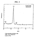
- FIG. 1 To illustrate the physical properties of protective layer 104 ( FIG. 1 ), reference is made to FIG. 1 in conjunction with FIGS. 3-4 .
- FIG. 3 an illustrative x-ray diffraction (XRD) spectrum of protective layer 104 deposited using a tantalum-base precursor in the form of TaCl 5 and a nitrogen plasma is shown. Even without atomic H, with only nitrogen plasma, protective layer was deposited.
- RBS analysis has shown that for an illustrative 1200 cycle deposition, 1.360x10 17 cm 2 of tantalum (Ta) atoms can be deposited with a nitrogen-to-tantalum (N/Ta) ratio of 1.3.
- the XRD pattern has been noted to indicate a Ta 3 N 5 phase
- other high nitrogen content TaN x phases such as Ta 4 N 5 and Ta 5 N 6 may also be present because all these phases have similar XRD peaks.
- the diffraction pattern is very close to the pattern known in the art to be obtained for Ta 3 N 5 phase deposited by tantalum penta-chloride (TaCl 5 ) and ammonia (NH 3 ).
- the chloride (Cl) content that was deposited using NH 3 is high at approximately 300°C by about 5 %.
- the Cl content was below 0.5%, which indicates that the efficiency of chloride (Cl) extraction of the nitrogen plasma is at least comparable to that of hydrogen plasma.
- copper (Cu) diffusion barrier properties were studied by thermal annealing, and obtaining sheet resistance and optical scattering results for an protective layer deposited to, for example, about 25 ⁇ thickness.
- copper (Cu) diffusion barrier failure was studied using two different in situ techniques, conducted simultaneously, while the sample was annealed in a forming gas at a temperature ramp rate of 3°C/s from 100 to 1000°C. Temperature was monitored using a K-type thermocouple, which was calibrated using eutectic melting points of various metals in contact with silicon (Si) for an accuracy of ⁇ 3°C.
- a chopped helium-neon (HeNe) laser beam was brought into the annealing chamber through a fiber optic cable and focused through a lens onto the sample surface at an incidence angle of 65° forming a spot size of 1 x 2 mm.
- the scattered intensities were measured using two bare fibers positioned at 50° and -20° allowing for measurement of lateral length scales of approximately 5 mm and 0.5 mm, respectively.
- lock-in amplifiers were used with silicon (Si) photodiodes and interference filters, which removed background light at other wavelengths. This optical scattering technique detects changes in the scattered intensity from surface roughness and also changes in index of refraction that the barrier failure may cause (e.g., coexistence of multiple phase composition domains).
- the second in situ technique used was a four-point probe sheet resistance measurement as a function of temperature.
- Four spring-loaded tantalum (Ta) probes arranged approximately in a square geometry maintained contact with the sample surface while 25 mA of current passes through two of the probes, and voltage is measured across the other two. This allowed for a relative sheet resistance measurement that is scaled using a room temperature, absolute measurement made with a fixed in-line four-point probe geometry.
- protective layer 104 has a thermal stability of greater than approximately 820°C, which is a much higher temperature compared to a substantially stoichiometric TaN ALD layer, which fails around 620°C (not shown). This indicates that the protective layer alone is a good diffusion barrier, but the high resistivity of the layer might be a problem in device application.
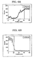
- FIGS. 5A-5B and 6A-6B show the results of number of test analysis on two different samples prepared on SiLK material.
- the samples were prepared by the deposition of ALD TaN x on 150 nm polycrystalline silicon to electrically isolate the silicon substrate during the sheet resistance analysis.
- the first sample ( FIGS. 5A and 6A ) was prepared using a conventional PE-ALD cubic TaN layer deposition using hydrogen and nitrogen mixture plasma.
- the second sample ( FIGS. 5B and 6B ) was generated according to the invention.
- the method included protective layer formation (nitrogen-only plasma) for 100 cycles followed by a substantially stoichiometric TaN layer formation (hydrogen and/or nitrogen) for 800 cycles.
- TEM Analytical transmission electron microscopy
- FIGS. 5A-5B Composition and thickness were determined by Rutherford backscattering spectrometry (hereinafter "RBS").
- FIG. 5A shows TEM analysis of deposition of tantalum-nitride on low-k material (e.g., SiLK) according to the prior art approach
- FIG. 5B shows TEM analysis of deposition of TaN x on low-k material (e.g., SiLK) according to the present invention.
- low-k materials such as SiLK are vulnerable when exposed to atomic H during plasma deposition.
- FIG. 5A illustrates the results of a hydrogen plasma to deposit substantially stoichiometric TaN layer 10 on SiLK layer 12. After deposition for 800 cycles, macroscopic delamination is observed for the films, resulting from the reactivity of SiLK with the hydrogen plasma. In particular, the interface is very rough between TaN layer 10 and SiLK layer 12, and mixing is clearly visible.
- FIG. 5B illustrates a TEM image of a second sample that was prepared according to the invention.
- low-k material 102 e.g., SiLK
- protective layer 104 successfully prevents the interaction of atomic hydrogen (H) with the SiLK layer 102 during the later formation of TaN diffusion barrier layer 108, and allows layer 108 to be successfully grown even on low-k material (e.g., SiLK) 102.
- H atomic hydrogen
- FIGS. 6A-6B illustrate micro energy dispersed x-ray (EDX) data that has been obtained for the samples shown in FIGS. 5A-5B , respectively.
- EDX micro energy dispersed x-ray
- FIG. 6A the conventional tantalum (Ta) profile shows severe intermixing and the interface is very diffuse.
- FIG. 6B shows the tantalum (Ta) profile generated by the present invention in which the profile shows very little, if any, intermixing and a very smooth interface.
- the invention impacts the field of semiconductor devices, and more particularly a method for forming a tantalum-nitride diffusion barrier region on such semiconductor devices.
Landscapes
- Engineering & Computer Science (AREA)
- Power Engineering (AREA)
- General Physics & Mathematics (AREA)
- Condensed Matter Physics & Semiconductors (AREA)
- Computer Hardware Design (AREA)
- Microelectronics & Electronic Packaging (AREA)
- Physics & Mathematics (AREA)
- Manufacturing & Machinery (AREA)
- Chemical & Material Sciences (AREA)
- Chemical Kinetics & Catalysis (AREA)
- General Chemical & Material Sciences (AREA)
- Chemical Vapour Deposition (AREA)
- Internal Circuitry In Semiconductor Integrated Circuit Devices (AREA)
- Electrodes Of Semiconductors (AREA)
Applications Claiming Priority (2)
| Application Number | Priority Date | Filing Date | Title |
|---|---|---|---|
| US10/709,865 US7211507B2 (en) | 2004-06-02 | 2004-06-02 | PE-ALD of TaN diffusion barrier region on low-k materials |
| PCT/US2005/018953 WO2005122253A2 (en) | 2004-06-02 | 2005-05-31 | PE-ALD OF TaN DIFFUSION BARRIER REGION ON LOW-K MATERIALS |
Publications (3)
| Publication Number | Publication Date |
|---|---|
| EP1756856A2 EP1756856A2 (en) | 2007-02-28 |
| EP1756856A4 EP1756856A4 (en) | 2010-02-17 |
| EP1756856B1 true EP1756856B1 (en) | 2013-07-24 |
Family
ID=35446788
Family Applications (1)
| Application Number | Title | Priority Date | Filing Date |
|---|---|---|---|
| EP05755089.9A Expired - Lifetime EP1756856B1 (en) | 2004-06-02 | 2005-05-31 | PE-ALD OF TaN DIFFUSION BARRIER REGION ON LOW-K MATERIALS |
Country Status (6)
| Country | Link |
|---|---|
| US (1) | US7211507B2 (enExample) |
| EP (1) | EP1756856B1 (enExample) |
| JP (1) | JP4791456B2 (enExample) |
| CN (1) | CN100447955C (enExample) |
| TW (1) | TWI345273B (enExample) |
| WO (1) | WO2005122253A2 (enExample) |
Families Citing this family (19)
| Publication number | Priority date | Publication date | Assignee | Title |
|---|---|---|---|---|
| US20050183740A1 (en) * | 2004-02-19 | 2005-08-25 | Fulton John L. | Process and apparatus for removing residues from semiconductor substrates |
| US7211507B2 (en) * | 2004-06-02 | 2007-05-01 | International Business Machines Corporation | PE-ALD of TaN diffusion barrier region on low-k materials |
| KR100552820B1 (ko) * | 2004-09-17 | 2006-02-21 | 동부아남반도체 주식회사 | 반도체 소자의 제조 방법 |
| US7482289B2 (en) * | 2006-08-25 | 2009-01-27 | Battelle Memorial Institute | Methods and apparatus for depositing tantalum metal films to surfaces and substrates |
| US7598170B2 (en) * | 2007-01-26 | 2009-10-06 | Asm America, Inc. | Plasma-enhanced ALD of tantalum nitride films |
| US7595270B2 (en) * | 2007-01-26 | 2009-09-29 | Asm America, Inc. | Passivated stoichiometric metal nitride films |
| JP5358893B2 (ja) * | 2007-04-03 | 2013-12-04 | 三菱電機株式会社 | トランジスタ |
| DE602007013386D1 (de) * | 2007-07-17 | 2011-05-05 | St Microelectronics Srl | Verfahren zur Herstellung eines kupferkompatiblen Phasenwechselspeicherelements und entsprechendes Phasenwechselspeicherelement |
| JP5551681B2 (ja) * | 2008-04-16 | 2014-07-16 | エーエスエム アメリカ インコーポレイテッド | アルミニウム炭化水素化合物を使用する金属炭化物膜の原子層堆積 |
| US20100055442A1 (en) * | 2008-09-03 | 2010-03-04 | International Business Machines Corporation | METHOD OF PE-ALD OF SiNxCy AND INTEGRATION OF LINER MATERIALS ON POROUS LOW K SUBSTRATES |
| CN101740369B (zh) * | 2008-11-19 | 2011-12-07 | 中国科学院微电子研究所 | 一种制备金属性金属氮化物薄膜的方法 |
| US9177826B2 (en) * | 2012-02-02 | 2015-11-03 | Globalfoundries Inc. | Methods of forming metal nitride materials |
| US8736056B2 (en) * | 2012-07-31 | 2014-05-27 | Taiwan Semiconductor Manufacturing Company, Ltd. | Device for reducing contact resistance of a metal |
| US8962473B2 (en) | 2013-03-15 | 2015-02-24 | Taiwan Semiconductor Manufacturing Co., Ltd. | Method of forming hybrid diffusion barrier layer and semiconductor device thereof |
| CN104109844B (zh) * | 2013-04-18 | 2016-07-06 | 中芯国际集成电路制造(上海)有限公司 | 一种基于原子层沉积技术的氮化钽薄膜的制作工艺 |
| KR102216575B1 (ko) | 2014-10-23 | 2021-02-18 | 에이에스엠 아이피 홀딩 비.브이. | 티타늄 알루미늄 및 탄탈륨 알루미늄 박막들 |
| CN106086809B (zh) * | 2016-06-17 | 2018-08-17 | 艾因斯(北京)钽应用科技有限公司 | 一种制备耐腐耐磨钽复合涂层的方法 |
| US10008558B1 (en) * | 2017-01-05 | 2018-06-26 | International Business Machines Corporation | Advanced metal insulator metal capacitor |
| US10032855B1 (en) | 2017-01-05 | 2018-07-24 | International Business Machines Corporation | Advanced metal insulator metal capacitor |
Family Cites Families (17)
| Publication number | Priority date | Publication date | Assignee | Title |
|---|---|---|---|---|
| GB2359825A (en) * | 1998-11-12 | 2001-09-05 | Applied Materials Inc | Improved tantalum-containing barrier layers for copper using high purity tantalum targets for sputtering |
| US6482733B2 (en) * | 2000-05-15 | 2002-11-19 | Asm Microchemistry Oy | Protective layers prior to alternating layer deposition |
| EP2293322A1 (en) * | 2000-06-08 | 2011-03-09 | Genitech, Inc. | Method for forming a metal nitride layer |
| KR100386034B1 (ko) * | 2000-12-06 | 2003-06-02 | 에이에스엠 마이크로케미스트리 리미티드 | 확산 방지막의 결정립계를 금속산화물로 충진한 구리 배선구조의 반도체 소자 제조 방법 |
| US6428859B1 (en) * | 2000-12-06 | 2002-08-06 | Angstron Systems, Inc. | Sequential method for depositing a film by modulated ion-induced atomic layer deposition (MII-ALD) |
| US20020117399A1 (en) * | 2001-02-23 | 2002-08-29 | Applied Materials, Inc. | Atomically thin highly resistive barrier layer in a copper via |
| US6916398B2 (en) * | 2001-10-26 | 2005-07-12 | Applied Materials, Inc. | Gas delivery apparatus and method for atomic layer deposition |
| US6972267B2 (en) * | 2002-03-04 | 2005-12-06 | Applied Materials, Inc. | Sequential deposition of tantalum nitride using a tantalum-containing precursor and a nitrogen-containing precursor |
| JP2004165634A (ja) * | 2002-08-15 | 2004-06-10 | Interuniv Micro Electronica Centrum Vzw | Ald表面処理のためのプラズマ処理 |
| JP3935428B2 (ja) * | 2002-12-27 | 2007-06-20 | 東京エレクトロン株式会社 | 成膜方法および成膜装置 |
| US20040175926A1 (en) * | 2003-03-07 | 2004-09-09 | Advanced Micro Devices, Inc. | Method for manufacturing a semiconductor component having a barrier-lined opening |
| JP4579157B2 (ja) * | 2003-03-25 | 2010-11-10 | 東京エレクトロン株式会社 | 処理装置及び切り替え機構 |
| JP2004311545A (ja) * | 2003-04-03 | 2004-11-04 | Matsushita Electric Ind Co Ltd | 半導体装置の製造方法及び高融点金属膜の堆積装置 |
| US7186446B2 (en) * | 2003-10-31 | 2007-03-06 | International Business Machines Corporation | Plasma enhanced ALD of tantalum nitride and bilayer |
| JP2005191290A (ja) * | 2003-12-25 | 2005-07-14 | Semiconductor Leading Edge Technologies Inc | 半導体装置の製造方法 |
| US7211507B2 (en) * | 2004-06-02 | 2007-05-01 | International Business Machines Corporation | PE-ALD of TaN diffusion barrier region on low-k materials |
| JP2006128542A (ja) * | 2004-11-01 | 2006-05-18 | Nec Electronics Corp | 電子デバイスの製造方法 |
-
2004
- 2004-06-02 US US10/709,865 patent/US7211507B2/en not_active Expired - Lifetime
-
2005
- 2005-05-30 TW TW094117722A patent/TWI345273B/zh not_active IP Right Cessation
- 2005-05-31 CN CNB2005800180516A patent/CN100447955C/zh not_active Expired - Lifetime
- 2005-05-31 WO PCT/US2005/018953 patent/WO2005122253A2/en not_active Ceased
- 2005-05-31 EP EP05755089.9A patent/EP1756856B1/en not_active Expired - Lifetime
- 2005-05-31 JP JP2007515460A patent/JP4791456B2/ja not_active Expired - Fee Related
Also Published As
| Publication number | Publication date |
|---|---|
| EP1756856A4 (en) | 2010-02-17 |
| CN101036217A (zh) | 2007-09-12 |
| WO2005122253A3 (en) | 2006-12-14 |
| CN100447955C (zh) | 2008-12-31 |
| TWI345273B (en) | 2011-07-11 |
| TW200540996A (en) | 2005-12-16 |
| WO2005122253A2 (en) | 2005-12-22 |
| JP4791456B2 (ja) | 2011-10-12 |
| EP1756856A2 (en) | 2007-02-28 |
| US7211507B2 (en) | 2007-05-01 |
| US20050269703A1 (en) | 2005-12-08 |
| JP2008502147A (ja) | 2008-01-24 |
Similar Documents
| Publication | Publication Date | Title |
|---|---|---|
| EP1756856B1 (en) | PE-ALD OF TaN DIFFUSION BARRIER REGION ON LOW-K MATERIALS | |
| Kim et al. | Diffusion barrier properties of transition metal thin films grown by plasma-enhanced atomic-layer deposition | |
| US6884466B2 (en) | Process for low-temperature metal-organic chemical vapor deposition of tungsten nitride and tungsten nitride films | |
| US6958174B1 (en) | Solid material comprising a thin metal film on its surface and methods for producing the same | |
| Heil et al. | Low-temperature deposition of TiN by plasma-assisted atomic layer deposition | |
| Kim et al. | High quality area-selective atomic layer deposition Co using ammonia gas as a reactant | |
| US20200131628A1 (en) | Method for forming molybdenum films on a substrate | |
| Longrie et al. | Plasma-enhanced ALD of platinum with O2, N2 and NH3 plasmas | |
| EP1261754A2 (en) | Methods for preparing ruthenium metal films | |
| Kovalgin et al. | Hot‐Wire Assisted ALD: A Study Powered by In Situ Spectroscopic Ellipsometry | |
| Törndahl et al. | Growth of copper (I) nitride by ALD using copper (II) hexafluoroacetylacetonate, water, and ammonia as precursors | |
| Kim et al. | Characteristics and compositional variation of TiN films deposited by remote PEALD on contact holes | |
| Sasinska et al. | Metallic Copper Thin Films Grown by Plasma‐Enhanced Atomic Layer Deposition of Air Stable Precursors | |
| US12252784B2 (en) | Copper halide layers | |
| US20010051215A1 (en) | Methods for chemical vapor deposition of titanium-silicon-nitrogen films | |
| Wang et al. | Smooth, low-resistance, pinhole-free, conformal ruthenium films by pulsed chemical vapor deposition | |
| Kim et al. | Characteristics of ALD tungsten nitride using B2H6, WF6, and NH3 and application to contact barrier layer for DRAM | |
| Li et al. | Characterization of WF 6/N 2/H 2 plasma enhanced chemical vapor deposited W x N films as barriers for Cu metallization | |
| Hinz et al. | Analysis of NbN thin film deposition by plasma-enhanced ALD for gate electrode application | |
| Vasilyev et al. | Surface Selective Growth of Ruthenium Films under Low-Temperature Pulsed CVD Conditions | |
| KR100968312B1 (ko) | 저-k 물질 상의 TaN 확산장벽 영역의 PE-ALD | |
| JP2003531291A (ja) | チタニウム−シリコン−窒素フィルムの化学的蒸着方法 | |
| GB2399350A (en) | Forming tungsten or tungsten containing films using krypton or xenon as sputter gas; Tungsten/tungsten nitride stacks | |
| Heil | Plasma-assisted atomic layer deposition of metal oxides and nitrides | |
| Zhang et al. | Electrical and mechanical characterization of chemical vapor deposition of tungsten on sputter‐deposited TiN layers |
Legal Events
| Date | Code | Title | Description |
|---|---|---|---|
| PUAI | Public reference made under article 153(3) epc to a published international application that has entered the european phase |
Free format text: ORIGINAL CODE: 0009012 |
|
| 17P | Request for examination filed |
Effective date: 20061129 |
|
| AK | Designated contracting states |
Kind code of ref document: A2 Designated state(s): AT BE BG CH CY CZ DE DK EE ES FI FR GB GR HU IE IS IT LI LT LU MC NL PL PT RO SE SI SK TR |
|
| AX | Request for extension of the european patent |
Extension state: AL BA HR LV MK YU |
|
| RIN1 | Information on inventor provided before grant (corrected) |
Inventor name: KIM, HYUNGJUN Inventor name: ROSSNAGEL, STEPHEN, M. Inventor name: DUNN, DERREN, N. Inventor name: SEO, SOON-CHEON |
|
| DAX | Request for extension of the european patent (deleted) | ||
| A4 | Supplementary search report drawn up and despatched |
Effective date: 20100118 |
|
| 17Q | First examination report despatched |
Effective date: 20100331 |
|
| REG | Reference to a national code |
Ref country code: DE Ref legal event code: R079 Ref document number: 602005040546 Country of ref document: DE Free format text: PREVIOUS MAIN CLASS: H01L0021283000 Ipc: H01L0021285000 |
|
| GRAP | Despatch of communication of intention to grant a patent |
Free format text: ORIGINAL CODE: EPIDOSNIGR1 |
|
| RIC1 | Information provided on ipc code assigned before grant |
Ipc: H01L 23/532 20060101ALI20130227BHEP Ipc: H01L 21/768 20060101ALI20130227BHEP Ipc: H01L 21/285 20060101AFI20130227BHEP |
|
| GRAS | Grant fee paid |
Free format text: ORIGINAL CODE: EPIDOSNIGR3 |
|
| GRAA | (expected) grant |
Free format text: ORIGINAL CODE: 0009210 |
|
| AK | Designated contracting states |
Kind code of ref document: B1 Designated state(s): AT BE BG CH CY CZ DE DK EE ES FI FR GB GR HU IE IS IT LI LT LU MC NL PL PT RO SE SI SK TR |
|
| REG | Reference to a national code |
Ref country code: GB Ref legal event code: FG4D |
|
| REG | Reference to a national code |
Ref country code: DE Ref legal event code: R081 Ref document number: 602005040546 Country of ref document: DE Owner name: GLOBALFOUNDRIES INC., KY Free format text: FORMER OWNER: INTERNATIONAL BUSINESS MACHINES CORPORATION, ARMONK, N.Y., US |
|
| REG | Reference to a national code |
Ref country code: CH Ref legal event code: NV Representative=s name: IBM RESEARCH GMBH ZURICH RESEARCH LABORATORY I, CH Ref country code: CH Ref legal event code: EP |
|
| REG | Reference to a national code |
Ref country code: AT Ref legal event code: REF Ref document number: 623861 Country of ref document: AT Kind code of ref document: T Effective date: 20130815 |
|
| REG | Reference to a national code |
Ref country code: IE Ref legal event code: FG4D |
|
| REG | Reference to a national code |
Ref country code: GB Ref legal event code: 746 Effective date: 20130816 |
|
| REG | Reference to a national code |
Ref country code: DE Ref legal event code: R096 Ref document number: 602005040546 Country of ref document: DE Effective date: 20130919 |
|
| REG | Reference to a national code |
Ref country code: DE Ref legal event code: R084 Ref document number: 602005040546 Country of ref document: DE Effective date: 20130807 |
|
| REG | Reference to a national code |
Ref country code: AT Ref legal event code: MK05 Ref document number: 623861 Country of ref document: AT Kind code of ref document: T Effective date: 20130724 |
|
| REG | Reference to a national code |
Ref country code: NL Ref legal event code: VDEP Effective date: 20130724 |
|
| REG | Reference to a national code |
Ref country code: LT Ref legal event code: MG4D |
|
| PG25 | Lapsed in a contracting state [announced via postgrant information from national office to epo] |
Ref country code: BE Free format text: LAPSE BECAUSE OF FAILURE TO SUBMIT A TRANSLATION OF THE DESCRIPTION OR TO PAY THE FEE WITHIN THE PRESCRIBED TIME-LIMIT Effective date: 20130724 Ref country code: IS Free format text: LAPSE BECAUSE OF FAILURE TO SUBMIT A TRANSLATION OF THE DESCRIPTION OR TO PAY THE FEE WITHIN THE PRESCRIBED TIME-LIMIT Effective date: 20131124 Ref country code: AT Free format text: LAPSE BECAUSE OF FAILURE TO SUBMIT A TRANSLATION OF THE DESCRIPTION OR TO PAY THE FEE WITHIN THE PRESCRIBED TIME-LIMIT Effective date: 20130724 Ref country code: SE Free format text: LAPSE BECAUSE OF FAILURE TO SUBMIT A TRANSLATION OF THE DESCRIPTION OR TO PAY THE FEE WITHIN THE PRESCRIBED TIME-LIMIT Effective date: 20130724 Ref country code: LT Free format text: LAPSE BECAUSE OF FAILURE TO SUBMIT A TRANSLATION OF THE DESCRIPTION OR TO PAY THE FEE WITHIN THE PRESCRIBED TIME-LIMIT Effective date: 20130724 Ref country code: PT Free format text: LAPSE BECAUSE OF FAILURE TO SUBMIT A TRANSLATION OF THE DESCRIPTION OR TO PAY THE FEE WITHIN THE PRESCRIBED TIME-LIMIT Effective date: 20131125 Ref country code: CY Free format text: LAPSE BECAUSE OF FAILURE TO SUBMIT A TRANSLATION OF THE DESCRIPTION OR TO PAY THE FEE WITHIN THE PRESCRIBED TIME-LIMIT Effective date: 20130717 |
|
| PG25 | Lapsed in a contracting state [announced via postgrant information from national office to epo] |
Ref country code: FI Free format text: LAPSE BECAUSE OF FAILURE TO SUBMIT A TRANSLATION OF THE DESCRIPTION OR TO PAY THE FEE WITHIN THE PRESCRIBED TIME-LIMIT Effective date: 20130724 Ref country code: SI Free format text: LAPSE BECAUSE OF FAILURE TO SUBMIT A TRANSLATION OF THE DESCRIPTION OR TO PAY THE FEE WITHIN THE PRESCRIBED TIME-LIMIT Effective date: 20130724 Ref country code: PL Free format text: LAPSE BECAUSE OF FAILURE TO SUBMIT A TRANSLATION OF THE DESCRIPTION OR TO PAY THE FEE WITHIN THE PRESCRIBED TIME-LIMIT Effective date: 20130724 Ref country code: NL Free format text: LAPSE BECAUSE OF FAILURE TO SUBMIT A TRANSLATION OF THE DESCRIPTION OR TO PAY THE FEE WITHIN THE PRESCRIBED TIME-LIMIT Effective date: 20130724 Ref country code: GR Free format text: LAPSE BECAUSE OF FAILURE TO SUBMIT A TRANSLATION OF THE DESCRIPTION OR TO PAY THE FEE WITHIN THE PRESCRIBED TIME-LIMIT Effective date: 20131025 |
|
| PG25 | Lapsed in a contracting state [announced via postgrant information from national office to epo] |
Ref country code: CY Free format text: LAPSE BECAUSE OF FAILURE TO SUBMIT A TRANSLATION OF THE DESCRIPTION OR TO PAY THE FEE WITHIN THE PRESCRIBED TIME-LIMIT Effective date: 20130724 |
|
| PG25 | Lapsed in a contracting state [announced via postgrant information from national office to epo] |
Ref country code: SK Free format text: LAPSE BECAUSE OF FAILURE TO SUBMIT A TRANSLATION OF THE DESCRIPTION OR TO PAY THE FEE WITHIN THE PRESCRIBED TIME-LIMIT Effective date: 20130724 Ref country code: RO Free format text: LAPSE BECAUSE OF FAILURE TO SUBMIT A TRANSLATION OF THE DESCRIPTION OR TO PAY THE FEE WITHIN THE PRESCRIBED TIME-LIMIT Effective date: 20130724 Ref country code: CZ Free format text: LAPSE BECAUSE OF FAILURE TO SUBMIT A TRANSLATION OF THE DESCRIPTION OR TO PAY THE FEE WITHIN THE PRESCRIBED TIME-LIMIT Effective date: 20130724 Ref country code: EE Free format text: LAPSE BECAUSE OF FAILURE TO SUBMIT A TRANSLATION OF THE DESCRIPTION OR TO PAY THE FEE WITHIN THE PRESCRIBED TIME-LIMIT Effective date: 20130724 Ref country code: DK Free format text: LAPSE BECAUSE OF FAILURE TO SUBMIT A TRANSLATION OF THE DESCRIPTION OR TO PAY THE FEE WITHIN THE PRESCRIBED TIME-LIMIT Effective date: 20130724 |
|
| PG25 | Lapsed in a contracting state [announced via postgrant information from national office to epo] |
Ref country code: IT Free format text: LAPSE BECAUSE OF FAILURE TO SUBMIT A TRANSLATION OF THE DESCRIPTION OR TO PAY THE FEE WITHIN THE PRESCRIBED TIME-LIMIT Effective date: 20130724 Ref country code: ES Free format text: LAPSE BECAUSE OF FAILURE TO SUBMIT A TRANSLATION OF THE DESCRIPTION OR TO PAY THE FEE WITHIN THE PRESCRIBED TIME-LIMIT Effective date: 20130724 |
|
| PLBE | No opposition filed within time limit |
Free format text: ORIGINAL CODE: 0009261 |
|
| STAA | Information on the status of an ep patent application or granted ep patent |
Free format text: STATUS: NO OPPOSITION FILED WITHIN TIME LIMIT |
|
| 26N | No opposition filed |
Effective date: 20140425 |
|
| REG | Reference to a national code |
Ref country code: DE Ref legal event code: R097 Ref document number: 602005040546 Country of ref document: DE Effective date: 20140425 |
|
| PG25 | Lapsed in a contracting state [announced via postgrant information from national office to epo] |
Ref country code: LU Free format text: LAPSE BECAUSE OF FAILURE TO SUBMIT A TRANSLATION OF THE DESCRIPTION OR TO PAY THE FEE WITHIN THE PRESCRIBED TIME-LIMIT Effective date: 20140531 |
|
| REG | Reference to a national code |
Ref country code: CH Ref legal event code: PL |
|
| PG25 | Lapsed in a contracting state [announced via postgrant information from national office to epo] |
Ref country code: CH Free format text: LAPSE BECAUSE OF NON-PAYMENT OF DUE FEES Effective date: 20140531 Ref country code: MC Free format text: LAPSE BECAUSE OF FAILURE TO SUBMIT A TRANSLATION OF THE DESCRIPTION OR TO PAY THE FEE WITHIN THE PRESCRIBED TIME-LIMIT Effective date: 20130724 Ref country code: LI Free format text: LAPSE BECAUSE OF NON-PAYMENT OF DUE FEES Effective date: 20140531 |
|
| REG | Reference to a national code |
Ref country code: IE Ref legal event code: MM4A |
|
| REG | Reference to a national code |
Ref country code: FR Ref legal event code: ST Effective date: 20150130 |
|
| PG25 | Lapsed in a contracting state [announced via postgrant information from national office to epo] |
Ref country code: IE Free format text: LAPSE BECAUSE OF NON-PAYMENT OF DUE FEES Effective date: 20140531 |
|
| PG25 | Lapsed in a contracting state [announced via postgrant information from national office to epo] |
Ref country code: FR Free format text: LAPSE BECAUSE OF NON-PAYMENT OF DUE FEES Effective date: 20140602 |
|
| PGFP | Annual fee paid to national office [announced via postgrant information from national office to epo] |
Ref country code: GB Payment date: 20150515 Year of fee payment: 11 |
|
| REG | Reference to a national code |
Ref country code: DE Ref legal event code: R081 Ref document number: 602005040546 Country of ref document: DE Owner name: GLOBALFOUNDRIES U.S. INC., SANTA CLARA, US Free format text: FORMER OWNER: INTERNATIONAL BUSINESS MACHINES CORPORATION, ARMONK, N.Y., US Ref country code: DE Ref legal event code: R082 Ref document number: 602005040546 Country of ref document: DE Representative=s name: GRUENECKER PATENT- UND RECHTSANWAELTE PARTG MB, DE Ref country code: DE Ref legal event code: R081 Ref document number: 602005040546 Country of ref document: DE Owner name: GLOBALFOUNDRIES U.S. INC., SANTA CLARA, US Free format text: FORMER OWNER: INTERNATIONAL BUSINESS MACHINES CORPORATION, ARMONK, NY, US Ref country code: DE Ref legal event code: R082 Ref document number: 602005040546 Country of ref document: DE Representative=s name: RICHARDT PATENTANWAELTE PARTG MBB, DE Ref country code: DE Ref legal event code: R081 Ref document number: 602005040546 Country of ref document: DE Owner name: GLOBALFOUNDRIES INC., KY Free format text: FORMER OWNER: INTERNATIONAL BUSINESS MACHINES CORPORATION, ARMONK, N.Y., US |
|
| REG | Reference to a national code |
Ref country code: DE Ref legal event code: R081 Ref document number: 602005040546 Country of ref document: DE Owner name: GLOBALFOUNDRIES U.S. INC., SANTA CLARA, US Free format text: FORMER OWNER: GLOBALFOUNDRIES US 2 LLC (N.D.GES.DES STAATES DELAWARE), HOPEWELL JUNCTION, N.Y., US Ref country code: DE Ref legal event code: R082 Ref document number: 602005040546 Country of ref document: DE Representative=s name: GRUENECKER PATENT- UND RECHTSANWAELTE PARTG MB, DE Ref country code: DE Ref legal event code: R082 Ref document number: 602005040546 Country of ref document: DE Representative=s name: RICHARDT PATENTANWAELTE PARTG MBB, DE Ref country code: DE Ref legal event code: R081 Ref document number: 602005040546 Country of ref document: DE Owner name: GLOBALFOUNDRIES INC., KY Free format text: FORMER OWNER: GLOBALFOUNDRIES US 2 LLC (N.D.GES.DES STAATES DELAWARE), HOPEWELL JUNCTION, N.Y., US |
|
| PG25 | Lapsed in a contracting state [announced via postgrant information from national office to epo] |
Ref country code: BG Free format text: LAPSE BECAUSE OF FAILURE TO SUBMIT A TRANSLATION OF THE DESCRIPTION OR TO PAY THE FEE WITHIN THE PRESCRIBED TIME-LIMIT Effective date: 20130724 |
|
| PG25 | Lapsed in a contracting state [announced via postgrant information from national office to epo] |
Ref country code: TR Free format text: LAPSE BECAUSE OF FAILURE TO SUBMIT A TRANSLATION OF THE DESCRIPTION OR TO PAY THE FEE WITHIN THE PRESCRIBED TIME-LIMIT Effective date: 20130724 Ref country code: HU Free format text: LAPSE BECAUSE OF FAILURE TO SUBMIT A TRANSLATION OF THE DESCRIPTION OR TO PAY THE FEE WITHIN THE PRESCRIBED TIME-LIMIT; INVALID AB INITIO Effective date: 20050531 |
|
| GBPC | Gb: european patent ceased through non-payment of renewal fee |
Effective date: 20160531 |
|
| PG25 | Lapsed in a contracting state [announced via postgrant information from national office to epo] |
Ref country code: GB Free format text: LAPSE BECAUSE OF NON-PAYMENT OF DUE FEES Effective date: 20160531 |
|
| REG | Reference to a national code |
Ref country code: DE Ref legal event code: R082 Ref document number: 602005040546 Country of ref document: DE Representative=s name: GRUENECKER PATENT- UND RECHTSANWAELTE PARTG MB, DE Ref country code: DE Ref legal event code: R081 Ref document number: 602005040546 Country of ref document: DE Owner name: GLOBALFOUNDRIES U.S. INC., SANTA CLARA, US Free format text: FORMER OWNER: GLOBALFOUNDRIES INC., GRAND CAYMAN, KY |
|
| P01 | Opt-out of the competence of the unified patent court (upc) registered |
Effective date: 20230412 |
|
| PGFP | Annual fee paid to national office [announced via postgrant information from national office to epo] |
Ref country code: DE Payment date: 20230404 Year of fee payment: 19 |
|
| REG | Reference to a national code |
Ref country code: DE Ref legal event code: R119 Ref document number: 602005040546 Country of ref document: DE |
|
| PG25 | Lapsed in a contracting state [announced via postgrant information from national office to epo] |
Ref country code: DE Free format text: LAPSE BECAUSE OF NON-PAYMENT OF DUE FEES Effective date: 20241203 |