EP1743376B1 - Active manipulation of light in a silicon-on-insulator (soi) structure - Google Patents
Active manipulation of light in a silicon-on-insulator (soi) structure Download PDFInfo
- Publication number
- EP1743376B1 EP1743376B1 EP05732990.6A EP05732990A EP1743376B1 EP 1743376 B1 EP1743376 B1 EP 1743376B1 EP 05732990 A EP05732990 A EP 05732990A EP 1743376 B1 EP1743376 B1 EP 1743376B1
- Authority
- EP
- European Patent Office
- Prior art keywords
- waveguide
- soi
- layer
- doped
- input
- Prior art date
- Legal status (The legal status is an assumption and is not a legal conclusion. Google has not performed a legal analysis and makes no representation as to the accuracy of the status listed.)
- Active
Links
- 239000012212 insulator Substances 0.000 title description 4
- 230000003287 optical effect Effects 0.000 claims description 142
- 229910021420 polycrystalline silicon Inorganic materials 0.000 claims description 71
- 229920005591 polysilicon Polymers 0.000 claims description 71
- 229910052710 silicon Inorganic materials 0.000 claims description 52
- 239000010703 silicon Substances 0.000 claims description 52
- XUIMIQQOPSSXEZ-UHFFFAOYSA-N Silicon Chemical compound [Si] XUIMIQQOPSSXEZ-UHFFFAOYSA-N 0.000 claims description 48
- 230000001902 propagating effect Effects 0.000 claims description 39
- 238000010168 coupling process Methods 0.000 claims description 26
- 238000005859 coupling reaction Methods 0.000 claims description 26
- 230000008878 coupling Effects 0.000 claims description 25
- 230000010287 polarization Effects 0.000 claims description 14
- 230000000295 complement effect Effects 0.000 claims description 7
- 238000007493 shaping process Methods 0.000 claims description 7
- 229910021421 monocrystalline silicon Inorganic materials 0.000 claims description 6
- 229910021417 amorphous silicon Inorganic materials 0.000 claims description 3
- 230000035945 sensitivity Effects 0.000 claims description 3
- 239000002210 silicon-based material Substances 0.000 claims description 3
- 238000012546 transfer Methods 0.000 claims description 3
- 239000010410 layer Substances 0.000 description 152
- 230000008859 change Effects 0.000 description 14
- 238000000034 method Methods 0.000 description 14
- 230000000694 effects Effects 0.000 description 11
- 238000012545 processing Methods 0.000 description 9
- 239000002019 doping agent Substances 0.000 description 6
- 230000010363 phase shift Effects 0.000 description 5
- 230000008569 process Effects 0.000 description 5
- 239000000758 substrate Substances 0.000 description 5
- 239000006185 dispersion Substances 0.000 description 4
- 239000000463 material Substances 0.000 description 4
- 239000000969 carrier Substances 0.000 description 3
- 238000010586 diagram Methods 0.000 description 3
- 238000004519 manufacturing process Methods 0.000 description 3
- 230000005374 Kerr effect Effects 0.000 description 2
- VYPSYNLAJGMNEJ-UHFFFAOYSA-N Silicium dioxide Chemical compound O=[Si]=O VYPSYNLAJGMNEJ-UHFFFAOYSA-N 0.000 description 2
- 238000010521 absorption reaction Methods 0.000 description 2
- 238000009825 accumulation Methods 0.000 description 2
- 230000008901 benefit Effects 0.000 description 2
- 230000015572 biosynthetic process Effects 0.000 description 2
- 238000005286 illumination Methods 0.000 description 2
- 230000000873 masking effect Effects 0.000 description 2
- 230000004048 modification Effects 0.000 description 2
- 238000012986 modification Methods 0.000 description 2
- 239000004065 semiconductor Substances 0.000 description 2
- 239000002344 surface layer Substances 0.000 description 2
- 230000009471 action Effects 0.000 description 1
- 230000004913 activation Effects 0.000 description 1
- 230000032683 aging Effects 0.000 description 1
- 238000003491 array Methods 0.000 description 1
- 230000005540 biological transmission Effects 0.000 description 1
- 230000000903 blocking effect Effects 0.000 description 1
- 230000001427 coherent effect Effects 0.000 description 1
- 238000004891 communication Methods 0.000 description 1
- 230000001934 delay Effects 0.000 description 1
- 230000001419 dependent effect Effects 0.000 description 1
- 238000013461 design Methods 0.000 description 1
- 238000001514 detection method Methods 0.000 description 1
- 230000005684 electric field Effects 0.000 description 1
- 238000005530 etching Methods 0.000 description 1
- 238000001914 filtration Methods 0.000 description 1
- 239000011521 glass Substances 0.000 description 1
- 239000007943 implant Substances 0.000 description 1
- 238000002513 implantation Methods 0.000 description 1
- 238000002347 injection Methods 0.000 description 1
- 239000007924 injection Substances 0.000 description 1
- 230000010354 integration Effects 0.000 description 1
- 238000002955 isolation Methods 0.000 description 1
- 230000031700 light absorption Effects 0.000 description 1
- 238000005259 measurement Methods 0.000 description 1
- 230000007246 mechanism Effects 0.000 description 1
- 239000002184 metal Substances 0.000 description 1
- 238000012544 monitoring process Methods 0.000 description 1
- 230000009022 nonlinear effect Effects 0.000 description 1
- 230000005693 optoelectronics Effects 0.000 description 1
- 230000000737 periodic effect Effects 0.000 description 1
- 229920000642 polymer Polymers 0.000 description 1
- 230000002441 reversible effect Effects 0.000 description 1
- 239000000377 silicon dioxide Substances 0.000 description 1
- 235000012239 silicon dioxide Nutrition 0.000 description 1
Images


Classifications
-
- H—ELECTRICITY
- H01—ELECTRIC ELEMENTS
- H01L—SEMICONDUCTOR DEVICES NOT COVERED BY CLASS H10
- H01L27/00—Devices consisting of a plurality of semiconductor or other solid-state components formed in or on a common substrate
- H01L27/02—Devices consisting of a plurality of semiconductor or other solid-state components formed in or on a common substrate including semiconductor components specially adapted for rectifying, oscillating, amplifying or switching and having potential barriers; including integrated passive circuit elements having potential barriers
- H01L27/12—Devices consisting of a plurality of semiconductor or other solid-state components formed in or on a common substrate including semiconductor components specially adapted for rectifying, oscillating, amplifying or switching and having potential barriers; including integrated passive circuit elements having potential barriers the substrate being other than a semiconductor body, e.g. an insulating body
-
- G—PHYSICS
- G02—OPTICS
- G02B—OPTICAL ELEMENTS, SYSTEMS OR APPARATUS
- G02B6/00—Light guides; Structural details of arrangements comprising light guides and other optical elements, e.g. couplings
- G02B6/10—Light guides; Structural details of arrangements comprising light guides and other optical elements, e.g. couplings of the optical waveguide type
- G02B6/12—Light guides; Structural details of arrangements comprising light guides and other optical elements, e.g. couplings of the optical waveguide type of the integrated circuit kind
- G02B6/12004—Combinations of two or more optical elements
-
- G—PHYSICS
- G02—OPTICS
- G02F—OPTICAL DEVICES OR ARRANGEMENTS FOR THE CONTROL OF LIGHT BY MODIFICATION OF THE OPTICAL PROPERTIES OF THE MEDIA OF THE ELEMENTS INVOLVED THEREIN; NON-LINEAR OPTICS; FREQUENCY-CHANGING OF LIGHT; OPTICAL LOGIC ELEMENTS; OPTICAL ANALOGUE/DIGITAL CONVERTERS
- G02F1/00—Devices or arrangements for the control of the intensity, colour, phase, polarisation or direction of light arriving from an independent light source, e.g. switching, gating or modulating; Non-linear optics
- G02F1/01—Devices or arrangements for the control of the intensity, colour, phase, polarisation or direction of light arriving from an independent light source, e.g. switching, gating or modulating; Non-linear optics for the control of the intensity, phase, polarisation or colour
- G02F1/015—Devices or arrangements for the control of the intensity, colour, phase, polarisation or direction of light arriving from an independent light source, e.g. switching, gating or modulating; Non-linear optics for the control of the intensity, phase, polarisation or colour based on semiconductor elements having potential barriers, e.g. having a PN or PIN junction
- G02F1/025—Devices or arrangements for the control of the intensity, colour, phase, polarisation or direction of light arriving from an independent light source, e.g. switching, gating or modulating; Non-linear optics for the control of the intensity, phase, polarisation or colour based on semiconductor elements having potential barriers, e.g. having a PN or PIN junction in an optical waveguide structure
-
- H—ELECTRICITY
- H01—ELECTRIC ELEMENTS
- H01L—SEMICONDUCTOR DEVICES NOT COVERED BY CLASS H10
- H01L21/00—Processes or apparatus adapted for the manufacture or treatment of semiconductor or solid state devices or of parts thereof
- H01L21/02—Manufacture or treatment of semiconductor devices or of parts thereof
- H01L21/04—Manufacture or treatment of semiconductor devices or of parts thereof the devices having potential barriers, e.g. a PN junction, depletion layer or carrier concentration layer
- H01L21/18—Manufacture or treatment of semiconductor devices or of parts thereof the devices having potential barriers, e.g. a PN junction, depletion layer or carrier concentration layer the devices having semiconductor bodies comprising elements of Group IV of the Periodic Table or AIIIBV compounds with or without impurities, e.g. doping materials
- H01L21/20—Deposition of semiconductor materials on a substrate, e.g. epitaxial growth solid phase epitaxy
-
- G—PHYSICS
- G02—OPTICS
- G02F—OPTICAL DEVICES OR ARRANGEMENTS FOR THE CONTROL OF LIGHT BY MODIFICATION OF THE OPTICAL PROPERTIES OF THE MEDIA OF THE ELEMENTS INVOLVED THEREIN; NON-LINEAR OPTICS; FREQUENCY-CHANGING OF LIGHT; OPTICAL LOGIC ELEMENTS; OPTICAL ANALOGUE/DIGITAL CONVERTERS
- G02F1/00—Devices or arrangements for the control of the intensity, colour, phase, polarisation or direction of light arriving from an independent light source, e.g. switching, gating or modulating; Non-linear optics
- G02F1/29—Devices or arrangements for the control of the intensity, colour, phase, polarisation or direction of light arriving from an independent light source, e.g. switching, gating or modulating; Non-linear optics for the control of the position or the direction of light beams, i.e. deflection
- G02F1/292—Devices or arrangements for the control of the intensity, colour, phase, polarisation or direction of light arriving from an independent light source, e.g. switching, gating or modulating; Non-linear optics for the control of the position or the direction of light beams, i.e. deflection by controlled diffraction or phased-array beam steering
-
- G—PHYSICS
- G02—OPTICS
- G02F—OPTICAL DEVICES OR ARRANGEMENTS FOR THE CONTROL OF LIGHT BY MODIFICATION OF THE OPTICAL PROPERTIES OF THE MEDIA OF THE ELEMENTS INVOLVED THEREIN; NON-LINEAR OPTICS; FREQUENCY-CHANGING OF LIGHT; OPTICAL LOGIC ELEMENTS; OPTICAL ANALOGUE/DIGITAL CONVERTERS
- G02F1/00—Devices or arrangements for the control of the intensity, colour, phase, polarisation or direction of light arriving from an independent light source, e.g. switching, gating or modulating; Non-linear optics
- G02F1/29—Devices or arrangements for the control of the intensity, colour, phase, polarisation or direction of light arriving from an independent light source, e.g. switching, gating or modulating; Non-linear optics for the control of the position or the direction of light beams, i.e. deflection
- G02F1/294—Variable focal length devices
Definitions
- the present invention relates to the active manipulation of light in a silicon-on-insulator (SOI) structure and, more particularly, to a silicon-insulator-silicon capacitive (SISCAP) structure that is doped in selected areas to provide the desired control of one or more optical beams propagating through the SOI structure.
- SOI silicon-on-insulator
- SISCAP silicon-insulator-silicon capacitive
- a planar lightwave circuit is the optical equivalent of an electronic chip, manipulating and processing light signals rather than electronic signals.
- a PLC is formed in a relatively thin layer of glass, polymer or semiconductor formed on a semiconductor substrate.
- the lightwave circuit itself is composed of one or more optical devices interconnected by optical waveguides, the waveguides functioning to guide the light from one optical device, to another and therefore considered as the optical equivalent of the metal interconnections in an electronic chip.
- the optical devices may comprise either passive optical devices, or active electro-optic devices, performing functions including, for example, reflection, focusing, collimating, beam splitting, wavelength multiplexing/demultiplexing, switching modulation and detection, and the like.
- the common planar optical devices formed in a silicon-on-insulator (SOI) structure use a relatively thick (> 3-4 ⁇ m) silicon surface waveguiding layer (hereinafter referred to as an "SOI layer"), so as to allow for relative ease of input/output coupling of a light signal to the SOI layer through methods such as edge illumination.
- SOI layer silicon surface waveguiding layer
- the need for edge-illumination coupling requires access to the edge of the chip, as well as the formation of an edge with a high surface quality (to prevent reflections and backscattering at the coupling interface).
- the fabrication of high definition structures is considered to be rather difficult in a relatively thick SOI layer (for example, forming "smooth" vertical sidewalls for waveguides, rings, mirrors, etc.).
- the thickness of the silicon also prevents the use of conventional CMOS simultaneously form both the electronic and optical components. Additionally, optical structures formed in such a relatively thick layer will tend to support the propagation of multiple optical modes, complicating the ability to provide transmission of only the 5 fundamental mode through the structure. Moreover, the relatively large thickness of the SOI layer also limits the speed of the electronic devices.
- the need remains to be able to actively manipulate the light within the SOI layer. More particularly, the need exists to perform various optical functions, such as turning, focusing, modulating, attenuating, deflecting, switching and selectively dispersing the light propagating sub-micron thick SOI layer, preferably utilizing conventional CMOS-compatible voltage levels to accomplish the active manipulation so that a common power supply may be used to control optical and electrical components formed on a common silicon substrate.
- the present invention relates to the active manipulation of light in a silicon-on-insulator (SOI) structure and, more particularly, to a silicon-insulator-silicon capacitive (SISCAP) structure that is doped in selected areas to provide the desired control over one or more optical beams propagating through the SOI structure.
- SOI silicon-on-insulator
- SISCAP silicon-insulator-silicon capacitive
- an SOI-based optical arrangement for actively manipulating a lightwave signal propagating in a silicon-insulator-silicon capacitive, SISCAP, waveguide, the SISCAP waveguide including a sub-micron surface silicon layer, SOI layer of the SOI based optical arrangement, a relatively thin dielectric layer overlying only a portion of the SOI layer and an upper silicon layer overlying only a portion of a combination of the SOI layer and the relatively thin dielectric layer, the arrangement for actively manipulating a lightwave signal comprising at least one doped area formed in the SISCAP waveguide area of the SOI layer, the at least one doped area having a first conductivity type, at least one doped area formed in the upper silicon layer so as to overlap at least a portion of the at least one doped area formed in the SOI layer to create an active optical region, the at least one doped area in the upper silicon layer having a second, opposite conductivity type, and a plurality of separate electrical contact regions each associated with an electrode
- the at least one doped area is formed in the SISCAP waveguide area of the SOI layer and the at least one doped area formed in the upper silicon layer are processed to form complementary doped regions of a desired shape in proximity to the relatively thin dielectric layer, leaving undoped areas in the SOI layer and the upper silicon layer in the active optical region, so as to form an active device region, the desired shape tailored such that a specific optical transfer function is achieved within the optical signal along the waveguide.
- the propagating light beam will be manipulated in a desired manner upon the application of a voltage to one or more of the separate electrical contact regions, the refractive index of the complementary doped regions will be modified to create regions for manipulating the properties of the propagating lightwave signal.
- the SISCAP structure includes the relatively thin (i.e., sub-micron) silicon surface layer (hereinafter referred to as "SOI layer") of an SOI structure, in combination with a relatively thin dielectric layer (referred to in the art as a "gate oxide") and an overlying silicon layer (usually comprising a form of polysilicon).
- SOI layer silicon surface layer
- the polysilicon layer and SOI layer are processed to form complementarily doped regions of a desired shape in proximity to the gate oxide; forming an active device region.
- the doped SISCAP structure functions as a conventional SOI-based waveguiding arrangement.
- the refractive indexes of the doped regions will be modified and, depending upon the shapes or the doped regions, the propagating light beam will be manipulated in a desired manner.
- the doped region(s) within the SOI layer and polysilicon layer may exhibit different shapes, and may be biased to different voltage levels. Indeed, the utilization of conventional CMOS processing/doping techniques allows for multiple doped regions to be formed in the SOI layer and/or the polysilicon layer so that optical elements such as gratings (and Fresnel lenses) can be formed.
- optical devices such as switches, polarization combiners, filters, ring resonators, Bragg gratings, Mach-Zehnder interferometers and the like may be formed and controlled. Indeed, a feedback path may be included between the optical output and the electrical bias input to perform optical control functions.
- Unstrained, pure silicon exhibits no linear electro-optic (Pockels) effect, and nonlinear effects such as the Franz-Keldysh and Kerr effects are very weak in pure silicon.
- an applied field in the range of 10 5 V/cm produces a change in the refractive index on the order of only about 10 -8 to 10 -5 .
- the most effective mechanisms to vary the refractive index/optical absorption of light in silicon are the free carrier effect ( ⁇ n ⁇ 10 -3 ) and the thermo-optic effect ( ⁇ n ⁇ 10 -4 ).
- the thermo-optic effect is defined as a change in the refractive index due to a change in the temperature of the silicon.
- the thermo-optic effect is rather slow (on the order of ⁇ 1MHz), and finds limited applications in today's high speed communication applications.
- the present invention is based upon the utilization of the free carrier effect in thin SOI (sub-micron) waveguide geometry.
- the waveguide geometry more particularly utilizes a SISCAP structure comprising a relatively thin oxide disposed over the surface (sub-micron) SOI layer, with a silicon layer (usually comprising a form of polysilicon) formed over the thin oxide in a manner to create an overlap with a portion of the SOI layer and form an active device region.
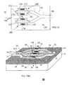
- FIG. 1 contains an isometric view
- FIG. 2 a cut-away side view of one such device. As shown, the device is formed within an SOI structure 10 including a silicon substrate 12, insulating layer 14, and sub-micron thick silicon surface layer (SOI layer) 16.
- SOI layer sub-micron thick silicon surface layer
- a relatively thin oxide (gate oxide) 18 is formed over a surface portion of SOI layer 16, and a polysilicon layer 20 is formed over gate oxide 18 and SOI layer 16 to form the illustrated overlapped structure.
- An insulating layer 26 is disposed adjacent to SOI layer 16 to provide for lateral confinement of the propagating optical mode.
- the same dielectric layer that is used to form the "gate oxide” for CMOS electronic devices on the common substrate may be used to form gate oxide 18 for the various active optical devices as described hereinbelow.
- similar voltage levels e.g., ⁇ 3.5 V
- layer 20 will be referred to as comprising "polysilicon”. It is to be understood that various types of silicon/polysilicon may be used to form this layer, including (but not limited to), amorphous silicon, grain-size enhanced polysilicon, grain-boundary passivated polysilicon, grain-boundary aligned polysilicon, single crystal silicon, substantially single crystal silicon and Gedoped silicon.
- the active switching and tuning functionality of the present invention is produced, as mentioned above, by free carrier modulation methods.
- the key to such optical manipulation is that the associated electronic control devices are integrated with the optical devices in the same SOI structure 10 so as to alter the index characteristics of the free carriers in active region 29 of SOI structure 10.
- One way to accomplish this is to fabricate an electronic device around an optical waveguide (e.g., a "rib” or effective index rib).
- the electronic device operation modifies the optical properties of the waveguide (the real and the imaginary parts of the refractive index) affecting the optical mode(s).
- the sub-micron dimensions of the device and the tight confinement of light enable the effective use of free carriers.
- the free carrier effect can be exploited using either the phase change of light due to the change in the real part of the index ( ⁇ n) or attenuation due to the imaginary part of the index ( ⁇ k) to provide free carrier modulation in any of the depletion, accumulation or inversion modes.
- active functionality can be achieved by appropriately doping selected portions of the waveguiding structure formed by the overlap of SOI layer 16, gate oxide 18 and polysilicon layer 20 (i.e., with the doping, thus forming active region 29) and placing electrodes in association with each doped portion (illustrated as a first electrode 22 associated with SOI layer 16 and a second electrode 24 associated with polysilicon layer 20).
- a two-dimensional electron (hole) gas (2DEG) is formed on both sides of gate oxide 18 within active region 29 by applying a defined voltage between electrodes 22 and 24.
- a collimated beam O is illustrated as passing through a slab waveguide formed in the SOI structure.
- triangular-shaped doped regions are formed in SOI layer 16 and polysilicon layer 20 in the vicinity of gate oxide 18. More particularly, a first doped region 17 is formed in SOI layer 16 in the area directly underneath gate oxide 18 and a second doped region 21 is formed in polysilicon layer 20 in the area directly above gate oxide 18, where regions 17 and 21 are formed to exhibit complementary doping types (typically, SOI layer 16 is p-doped and polysilicon layer 20 is n-doped, although the reverse may be used as well).
- CMOS process techniques may be used to sequentially mask and implant SOI layer 16 and polysilicon layer 20 to form the desired patterns in the doped areas, while also providing the necessary doping profile and overlap in the vertical direction between doped regions 17 and 21.
- electrodes 22 and 24 are located at a predetermined distance from active region 29 - the region of optical signal propagation and manipulation, so as to minimize optical loss.
- a pair of heavily-doped regions 23 and 25 are formed in association with electrodes 22 and 24 to provide the necessary electrical contact to SOI layer 16 and polysilicon layer 20, respectively, where these regions are also in contact with doped regions 17 and 21 to form the required electrical signal path. While the remote location of electrodes 22 and 24 with respect to the optical signal path will reduce loss, the requisite spacing results in limiting the operational speed of the active device.
- the shape of the doped region(s) can be tailored such that a specific optical transfer function ("OTF") is achieved within the optical signal propagating along the waveguide (i.e., "active manipulation of light”).
- OTF optical transfer function
- a variety of such shapes will be discussed hereinbelow in association with the description of various active optical devices. It is to be understood that the active devices discussed below are exemplary only of the principles of the present invention; virtually any possible shape/doping profile may be used in an SOI-based SISCAP structure in order to form active optical devices of the present invention. Indeed, a thorough discussion of various SISCAP structures and doping variations may be found in commonly-assigned US Patent No. 6,845,198 .
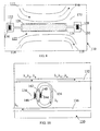
- FIGs. 3(a) - (c) illustrate (in a top view) three different activation circumstances for an active SISCAP optical device 30 of the present invention.
- active SISCAP device 30 comprises a first doped region 32 shaped to function as a lens and a second lens-shaped doped region 34 separated from first lens region 32 by a predetermined isolating gap g. Similar to the generic structure of FIGs.
- first doped lens region 32 includes an n-types doped area 31 formed in SOI layer to and a p-type doped area 33 formed in polysilicon layer 20 (or complementarily doped, as discussed above), where each area 31, 33 is properly shaped (using conventional CMOS masking and dopant implantation processes) to provide the desired lensing function.
- Second doped lens region 34 similarly comprises an n-type doped area 35 in SOI layer 16 and a p-type doped area 37 in polysilicon layer 20 that combine to form the predetermined lens shape.
- a first pair of electrodes 36, 38 is used to contact doped area 31 and doped area 33, respectively, in the region of first lens 32.
- a second pair of electrodes 40, 42 is used to contact doped area 35 and doped area 37, respectively, in the region of second lens 34.
- a heavily-doped contact area is formed in the silicon material directly underneath each electrode, so as to form a high conductivity connection.
- first lens 32 and second lens 34 can be controlled.
- the lensing structure behaves as a passive optical waveguiding device, since the back-to-back lens structures will nullify each other's dispersion.
- the index of the doped regions will change, resulting in shaping the phase front of the optical mode and accomplishing the focusing function.
- FIG. 3(a) when no voltage is applied to any of the electrodes, the lensing structure behaves as a passive optical waveguiding device, since the back-to-back lens structures will nullify each other's dispersion.
- the index of the doped regions will change, resulting in shaping the phase front of the optical mode and accomplishing the focusing function.
- a first set of voltages (illustrated as V + and V - ) is applied to electrical contacts 40 and 42, reducing the effective index within second lens 34 such that a propagating beam is focused at a point A.
- V + and V - the respective voltage levels
- V ++ and V -- in FIG. 3(c) the focus can be moved to a point B, as shown.
- the application of voltages to first lens 32 will result in a different type of beam shaping.
- any collection of lenses may be used to provide the desired optical beam shaping in accordance with the present invention, including beam expansion as well as beam focusing.
- the ability to dynamically adjust the focusing properties of waveguide lenses allows for a propagating lightwave to be focused into relatively narrow (sub-micron) single mode waveguides, an important need in future SOI-based opto-electronic systems.
- the ability to actively modify the focal point of a lensing arrangement allows for adjustments to be made as needed for process variations, ambient temperature variations, aging variations, and the like.
- FIGs. 4(a) - (c) illustrate one such beam deflector 50 formed in accordance with the present invention.
- a pair of prism-shaped doped regions 52 and 54 are formed within active waveguide region 29 in the overlap of SOI layer 16, gate oxide 18 (as shown in FIGs. 1 and 2 ) and polysilicon layer 20.
- the prisms are oriented, as shown in the figures, such that an angled facet 56 of first prism-shaped region 52 is adjacent to angled facet 58 of second prism-shaped region 54 (with a necessary isolation gap g therebetween).
- the doped regions are created by properly masking and implanting predefined areas of SOI layer 16 and polysilicon layer 20.
- SOI layer 16 may be implanted with an n-type dopant within a portion of active region 29 contiguous with gate oxide 18 to form a first doped region 61.
- Polysilicon layer 20 may be implanted with a p-type dopant in a portion of action region 29 to form a second doped region 63 (the converse arrangement is possible, with SOI layer 16 processed to include p-type areas and polysilicon layer 20 to include n-type areas).
- a first pair of electrodes 60, 62 is illustrated as associated with first prism region 52, with electrode 60 disposed to modify the index within doped region 61 of SOI layer 16 and electrode 62 disposed to modify the index within doped region 63 of polysilicon layer 20.
- a second pair of electrodes 64, 66 is associated with second prism region 54, with electrode 64 disposed to control the index of a doped region 65 within SOI layer 16 and electrode 66 disposed to control the index of a doped region 67 within polysilicon layer 20.
- electrode 64 disposed to control the index of a doped region 65 within SOI layer 16
- electrode 66 disposed to control the index of a doped region 67 within polysilicon layer 20.
- FIGs. 4(a) - (c) the manipulation of a light beam L in terms of deflection is illustrated as being controlled by voltages applied between the electrodes associated with each prism region.
- no voltage is applied to any electrode, and the prism structure behaves as a passive optical waveguiding device, without any change in the propagating optical mode(s) at light beam L travels through doped prism regions 52 and 54, since the back-to-back prism structures will nullify each other's dispersion.
- appropriate voltages are applied to electrodes 60 - 66, the index of the various doped areas 61, 63, 65 and 67 is changed, resulting in deflection of the optical mode(s). Referring to FIG.
- Bragg gratings are well-known optical structures that are used to perform various optical functions, such as optical filtering, group velocity dispersion control, attenuation and the like.
- the fundamental principle behind Bragg gratings is the small, periodic variation in the index (mode index) or propagation constant in a waveguide caused by a grating structure disposed in the waveguide, which then leads to a resonant condition for diffraction of certain wavelengths. Different wavelengths can be selected by changing the grating period.
- the wavelengths of interest are selected to pass through the grating structure, with the remaining wavelengths reflected back along the waveguide.
- different wavelengths are selected to diffract "out" of the grating (typically in a direction normal to the grating, but any other angle may be chosen), thus forming a wavelength selective device.
- Bragg gratings may be formed by including properly doped grating elements within SOI layer 16 and polysilicon layer 20 of the SISCAP structure as discussed above.
- FIG. 5 illustrates an exemplary transmissive Bragg grating structure, formed in accordance with the present invention.
- a Bragg grating 70 is illustrated as comprising a plurality of doped grating elements 72 disposed along the length of a waveguide region 74 formed in the active region 29 of a SISCAP structure by the overlap of SOI layer 16, gate oxide 18 and polysilicon layer 20, as discussed above.
- a first plurality of electrodes 76 is illustrated as associated with a like plurality of doped areas 77 within SOI layer 16, with a separate, individual electrode 76-i used to control each doped area 77-i.
- a second plurality of electrodes 78 is illustrated as associated with a like plurality of doped areas 79 within polysilicon layer 20 such that the combination of doped areas 77 with doped areas 79 form the desired grating elements 72.
- the grating period of Bragg grating 70 may be modified in accordance with the present invention to provide the active manipulation of a propagating light beam. For example, by energizing every other electrode in first and second pluralities 76 and 78, a first Bragg grating period ⁇ 1 is realized, as shown in FIG. 5 . This particular period will then allow an associated wavelength ⁇ 1 to be transmitted along waveguide 74, with all remaining wavelengths reflected.
- a different Bragg grating resonant wavelength will result. In this case, as also illustrated in FIG. 5 , Bragg grating 72 will exhibit a grating period of ⁇ 2 allowing a different associated wavelength ⁇ 2 to be transmitted.
- an active Bragg grating structure 70 may be formed by adjusting the voltages applied to each separate, individual grating element 76 and 78, where the voltage adjustments will modify the index of the associated grating elements and form the desired Bragg structure.
- a Bragg grating is a resonant device
- the ability to "tune" Bragg grating 70 in accordance with the present invention allows for the grating to be utilized with signals of an unknown "wavelength", adjusting the resonant cavity length accordingly. Indeed, variations in signal wavelength as a function of, for example, temperature or processing variations may be compensated by utilizing detectors at the input and output of the grating to measure the input/output power ratio and tuning the resonator based on this measurement.
- detectors may be disposed at the input and output of Bragg grating 70 to determine the particular wavelength that is transmitted by the given structure.
- the Bragg grating can be "tuned” and monitored such that a lightwave signal at a desired wavelength is produced. Since fabrication process variations may alter the wavelength associated with a given Bragg grating, the ability to "tune" the structure is considered a significant aspect of the present invention.
- the grating structure itself may be "chirped” (i.e., different spacing between adjacent elements), "apodized” (i.e., different envelope shape for grating structure), "blazed” (i.e., elements angled with respect to optical axis), or any combination of the above, where the characteristics of such Bragg gratings are well-known to those skilled in the art and may find a variety of uses as active, tunable devices.
- FIG. 6 illustrates an alternative Bragg grating structure 700, where this particular structure is based on a "rib" waveguide confinement region O, as shown, where the rib is formed by the appropriate truncation of SOI layer 16 and polysilicon layer 20, as described below.
- a dielectric region 710 (comprising, for example, silicon dioxide) is disposed in the plane of SOI layer 16 and used to assist in the lateral confinement of the optical signal within active region 29 by truncating the extent of the silicon material forming SOI layer 16.
- Overlying polysilicon layer 20 is processed so as to remove that portion disposed over SOI layer 16 beyond gate oxide 18. This is illustrated by sidewall 720 as shown in FIG.
- the ability for such a waveguide structure to be formed is considered to be an important component of providing a structure capable of supporting only the fundamental mode of a lightwave signal (thus preventing higher-order modes from appearing during signal propagation).
- a first plurality of doped regions 730 within SOI layer 16 are utilized to form a portion of the "grating" structure, similar to Bragg grating 70 of FIG. 5 .
- a second plurality of doped regions 740 are formed within polysilicon layer 20 and used to define the remaining portion of the grating structure for Bragg grating 700.
- a first plurality of electrical contacts 750 is used to control separate ones of doped regions 730 and a second plurality of electrical contacts 760 is used to similarly control separate ones of doped regions 740, providing the same type of Bragg grating adjustment/tunability as discussed above in association with FIG. 5 .
- the free carrier effect can be exploited using both the phase change (real index, n) and absorption (imaginary index k).
- the active manipulation of light can be realized by changing the phase of the optical mode(s) passing through the device structure.
- amplitude modulation can be achieved using a version of a Mach-Zehnder interferometer (MZI) in which interference is produced between two coherent lightwaves that have a definite phase difference between them.
- MZI Mach-Zehnder interferometer
- FIG. 7 illustrates an exemplary MZI 80 formed in accordance with the present invention, with FIG. 7(a) illustrating a top view and FIG. 7(b) illustrating an isometric view.
- MZI 80 includes that includes active devices in both arms to control its performance.
- MZI 80 is illustrated as including an input waveguiding section 82 and an input Y-splitter 84 so as to divide the input signal into two separate optical paths (arms) 86 and 88.
- the particular inventive arrangement as illustrated in FIG. 7 utilizes a properly patterned polysilicon layer 20 to form the desired "Y-splitter” and "arm” geometries in accordance with the "rib"-type structures discussed above.
- polysilicon layer 20 can be tapered at the input (see portion 20-T) of MZI 80 to reduce reflections and enhance coupling efficiency into MZI 80.
- polysilicon layer 20 may be properly shaped at the output of MZI 80 (see portion 20-O) to determine the divergence angle of the exiting beam.
- output portion 20-O of polysilicon layer 20 can be patterned so that the exiting beam matches the collimating optics (not shown) disposed beyond MZI 80, resulting in very little signal loss.
- An important aspect of using a patterned polysilicon layer 20 to form this structure is that the vertical and lateral dimensions of active region 29 can be controlled such that the MZI will support the propagation of only the fundamental mode of the applied lightwave signal. The ability to support only the fundamental mode is particularly important at Y-combiner 90 such that single mode operation is supported from the input throughout the output of the MZI.
- a first active device 94 formed in accordance with the present invention, is illustrated as disposed along a section of first arm 86 and a second active device 96 is illustrated as disposed along a section of second arm 88.
- first active device 94 is illustrated as including a first doped area 91 in SOI layer 16 and a second doped area 93 in polysilicon layer 20.
- second active device 96 is formed to include a first doped area 95 in SOI layer 16 and a second doped area 97 in polysilicon layer 20. In the particular embodiment of FIGs.
- doped areas 91, 93, 95 and 97 are illustrated as rectangular in shape.
- the ends of the polysilicon rectangles may be tapered (along the direction of signal propagation) to minimize reflections.
- a first electrical contact 100 for first active device 94 is made to doped area 91 of SOI layer 16 and a second electrical contact 102 is made to doped area 93 of polysilicon layer 20.
- a pair of electrical contacts 104 and 106 are similarly associated with doped areas 95 and 97 of second active device 96.
- the propagation constant; ⁇ of the propagating optical mode can be changed by free carrier injection or removal in active devices 94 and/or 96.
- the output intensity of MZI 80 can be precisely controlled by using "fine tuning" control over ⁇ (propagation constant) and hence in another embodiment an inventive can use the MZI as a dynamic gain equalizer or variable optical attenuator (VOA), with appropriate feedback control.
- VOA variable optical attenuator
- the active MZI of the present invention may operate in accumulation mode, depletion mode or inversion mode, depending upon the dopant conductivity types used in active regions 91, 93, 95 and 97, as well as the polarity of the voltages applied thereto.
- multiple arrays of MZI's, either cascaded or parallel, may be formed using conventional CMOS processing techniques and used to provide more complicated signal control. All of these variations are considered to fall within the scope of the present invention.
- FIG. 8 illustrates (in a top view) an exemplary active optical switch 110 formed in accordance with the principles of the present invention.
- Switch 110 formed in a SISCAP structure as described above, comprises a pair of single mode input waveguides 112, 114 and a pair of single mode output waveguides 116, 118, with a central waveguiding area 120 formed therebetween.
- each waveguide section may be formed in only SOI layer 16.
- each waveguide section may consist of the "SISCAP" structure of SOI layer 16, gate oxide 18 and polysilicon layer 20.
- an active device region 122 is illustrated as disposed over central waveguiding area 120 (in this case, device region 122 being rectangular in form) and includes complementarily doped areas within SOI layer 16 and polysilicon layer 20.
- a first doped region 124 is formed SOI layer 16 and a second doped region 126 is formed in SOI layer 20, resulting in the overlapped rectangular structure as shown in FIG. 8 .
- a first electrical contact area 128 is associated with doped region 124 of SOI layer 16 (and includes a heavily doped contact area 130).
- a second electrical contact area 132 is associated with doped region 126 of polysilicon layer 20, and similarly includes a heavily doped contact area 134.
- an input, fundamental mode signal propagating through input waveguide 112 will generate both the fundamental mode and first order mode as the signal enters central waveguiding area 122.
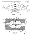
- FIG. 9 illustrates, in a top view, an alternative active optical switch structure 200 where separate active optical devices may be included along parallel arms of the switch to control the switching function.
- switch 200 is illustrated as including an input waveguiding section 210, in this case formed within SOI layer 16, and then branches into a Y-splitter section 211 to form a pair of parallel switch arms 212 and 214.
- the various passing waveguiding portions may be formed only in SOI layer 16, or in the combination of SOI layer 16, gate oxide 18 and polysilicon layer 20.
- a separate active optical device is disposed over a region of each arm and using to control the effective path length "seen" by a propagating optical signal and thus introduce any desired phase shift between the two propagating beams.
- a first active device 220 is formed by doping a selected portion 222 of SOI layer 16 in a predetermined area.
- a polysilicon region 224 is formed over doped SOI portion 222 and infused with a complementary doping material to form active device 220.
- polysilicon region 224 is patterned to include an input tapered region 223 and output tapered region 225.
- a pair of electrical contacts 226, 228 are disposed in relation to doped regions 222 and 224 and used to modify the electrical potential through active device 220 and therefore provide an arrangement to control the "length" of arm 212.
- a second active device 230 is formed within a portion of second waveguide arm 214 and can be controlled by electrodes 232 and 234 to likewise modify the optical path length "seen" by a propagating signal. Therefore, by controlling the voltages applied to first and second active devices 220, 230, various phase delays can be introduced into each signal path. The phase difference between the optical signals, upon entering directional coupling arrangement 240, will therefore control the power level of the signals appearing along separate output arms 250 and 252 of active switching device 200.
- FIG. 10 illustrates an exemplary add/drop ring resonator 130 including a single mode waveguiding structure 132 and associated ring resonator 134, formed (as discussed above) in either SOI layer 16 or the combination of SOI layer 16, gate oxide 18 and polysilicon layer 20.
- the physical dimensions of ring resonator 134 dictate a particular wavelength (or range of wavelengths) that may be out-coupled from a multi-wavelength signal propagating along waveguide 132 (when used in the "drop" mode).
- this aspect is illustrated by a signal propagating at a wavelength of ⁇ 2 being coupled into ring resonator 134, and thereafter launched (in a counter-propagating direction) along a second single mode waveguide 136.
- an optical signal at a predetermined wavelength that is coupled from second waveguide 136 into ring resonator 134 will subsequently be coupled into waveguide 132 (when used in the "add" mode).
- the wavelength sensitivity of ring resonator 134 may be modified by including an active device section 138 along a portion thereof.
- active device section 138 comprises a first doped area 140 within a particular portion of SOI layer 16 and an overlying doped area 142 (doped to exhibit a complementary dopant type) formed in polysilicon layer 20.
- a pair of electrical contacts 144 and 146 are coupled to doped regions 140 and 142 of SOI layer 16 and polysilicon layer 20, respectively.
- the optical path length of ring resonator 134 will be modified, thus changing the particular wavelength(s) that can be coupled into/out of waveguide section 132.
- a tunable optical modulator may be formed.
- a ring resonator structure of the present invention may comprise a plurality of separate rings, each formed using similar processing techniques.
- the separate rings are disposed along a waveguide, with each ring appropriate sized and “tuned” to add/drop a different wavelength.
- a plurality of rings may be "stacked" in a direction normal to the waveguide, providing greater and greater wavelength selectivity between adjacent rings. Any of these variations are possible and may be provided by conventional, well-known CMOS processing techniques. Indeed, it is possible to combine one of the active switch arrangements discussed above with the inventive active ring resonator to form a structure that provides tunable wavelength coupling into a ring resonator.
- Another monolithic structure may comprise the pairing of a ring resonator (or Bragg grating) with a modulator.
- Thin (i.e., sub-micron) SOI waveguides are known to be polarization dependent and as a result the incoming signal polarizations need to be rotated accordingly.
- the TM component of the signal must be rotated to the TE polarization mode, and then recombined with the "true" TE mode to form the desired signal.
- the phases of the two beams are different, the resultant recombined beam can suffer loss (due to interference effects).
- One method to minimize this loss is to use a polarization combiner formed in accordance with the present invention.
- FIG. 11 illustrates one such exemplary on-chip active polarization combiner 150 formed in a SISCAP structure (as discussed above) in accordance with the present invention.
- an original TE polarization component is coupled into a first waveguide 152, waveguide 152 formed from the SISCAP structure described above that includes a combination of SOI layer 16, gate oxide 18 and polysilicon layer 20 to form active region 29.
- the rotated" TE mode signal (that had originally been of TM polarization) is applied as an input to a second waveguide 154, where waveguides 152 and 154 are joined in a Y-combiner portion 156 and subsequently coupled into an output waveguide 158.
- Active phase shifting between the two polarized signals is accomplished in accordance with the present invention by utilizing an active optical device along either one or both of waveguides 152, 154.
- a first active device 160 is illustrated as formed along a portion of first waveguide 152 and a second active device 162 is illustrated as formed along a portion of second waveguide 154.
- active devices 160, 162 are formed by properly doping selected areas of SOI layer 16 and polysilicon layer 20.
- first active device 160 includes a doped area 161 in SOI layer 16 and a similarly-shaped doped area 163 in polysilicon layer 20.
- Second active device 162 includes similarly formed doped areas 165 and 167.
- a first pair of electrical contacts 170, 172 are illustrated as associated with doped areas 161, 163 of first active device 160 and a second pair of electrical contacts 174, 176 are illustrated as associated with doped areas 165, 167 of second active device 162.
- the optical path lengths of waveguides 152 and 154 can be modified, thus adjusting the phase shift between the TE and "rotated" TE components propagating therealong. Careful adjustment of these voltages can therefore be used to properly combine the signals along output waveguide 158 with little, if any, signal loss.
- FIG. 12 illustrates, in an isometric view, an exemplary active Fabry-Perot (FP) device 180 formed in accordance with the present invention, where the inclusion of an active optical device 182 in cavity region 184 of FP device 180 can be used to modify the optical path length (and therefore, the resonance) of FP device 180.
- FP device 180 includes an input grating structure 186 formed by etching a portion of polysilicon layer 20, as shown.
- An output grating structure 188 is similarly formed in polysilicon layer 20, where cavity region 184 is defined as the extent of the waveguiding region between input grating structure 186 and output grating structure 188.
- the wavelength sensitivity of FP device 180 can be adjusted. Further, by using active device 182 to tune TP device 180 in to and out of resonance, an optical modulator may be formed.
- active device 182 includes a first doped area 190 within SOI layer 16 and a second doped area 192 within polysilicon layer 20. Electrodes 194 and 196 are coupled, respectively, to doped areas 190 and 192, where the application of a voltage potential between these electrodes will affect the optical path length within cavity region 184.
- Input and output detectors (not shown), when used in combination with FP device 180 allow for feedback and control of the resonant wavelength within the cavity by allowing the applied voltages to be adjusted in accordance with the measured values at the input and output of the device.
- An important class of optical filters is represented by "arrayed waveguide gratings" (AWGs).
- AWG is defined as a planar structure comprising a number of array waveguides whose arrangement emulates the functionality of a diffraction grating.
- AWGs are commonly used as multiplexers or demultiplexers, and can also be designed to perform as passive, wavelength selective, strictly non-blocking cross-connects for sets of optical channels.
- AWGs can simultaneously operate as a multiplexer and demultiplexer by distributing and recombining multiple frequencies entering any number of input ports into any of a multiple number of output ports.
- One problem with prior art AWG structures is the need to carefully control the path lengths between the couplers forming the structure. In a planar integrated optics structure, this requirement often necessitated the use of arc-like optical paths, a difficult geometry to manufacture with any great consistency.
- an active AWG structure 400 as formed in accordance with the present invention may utilize a plurality of active devices, one device disposed along each signal path, to provide the desired variations in optical path length without resorting to changing the physical paths at all.
- FIG. 13 illustrates AWG 400 as including an input coupling region 410 and an output coupling region 420, where AWG 400 is generally formed within layers 16, 18 and 20 of the SISCAP structure as discussed above.
- Input coupling region 410 is illustrated as comprising a single input waveguide 412 and a plurality of N separate output waveguides 414, where various different wavelengths will appear at separate ones of output waveguides 414.
- Output coupling region 420 is illustrated as comprising a plurality of N input waveguides 422, each coupled in a one-to-one relationship with the plurality of N output waveguides 414 from input coupling region 410. Output coupling region 420 further comprises a plurality of N output waveguides 424.
- each waveguide 430-I is shown as including a separate active optical device 440.
- each active device is essentially identical in form, although this is not a required.
- active optical device 240 comprises a first doped region 441 within SOI layer 16 and an overlying (similarly shaped) second doped region 443 within polysilicon layer 20.
- active device 440 is specifically called out in the arrangement of FIG. 13 , although each device comprises similar elements.
- a first electrical contact 442 is coupled to and controls first doped region 241 within SOI layer 16 and a second electrical contact 444 is coupled to and controls second doped region 443 within polysilicon layer 20.
- first electrical contact 442 and second electrical contact 444 the optical path length of the associated waveguide 430 will be modified, providing the desired diffraction effect.
- each separate active device 430 in AWG structure 400 is controlled by a different voltage potential, so as to create a plurality of different path lengths to form the diffraction grating.
- the voltages may be "tuned” or changed to modify the properties of AWG 400, as needed.
- the operational wavelengths associated with desired diffraction effect can simply be changed by modifying the applied voltages.
- wavelength-selective routing between different output ports can be achieved by modifying the voltages applied to the various active devices.
- the ability to provide wavelength-selective routing and switching in such an arrayed waveguide structure is considered to be a significant advance of the state of the art.
- any modification in the operation of an AWG structure necessitated a complete change in the physical layout and design.
- the operation of AWG 400 can be controlled, with feedback signals from one or more of these waveguides used to adjust, in real time, the voltages applied to associated ones of active devices 430.
- planar optical devices may be formed as active devices in a SISCAP structure in accordance with the present invention.
- Fresnel lenses may be "tuned” using the doped device structure as described above.
- An active, adjustable multimode interference (MMI) splitter as discussed in our co-pending application No. 10/830,571 filed December 23,2004 , may also be formed, where one or more active devices are formed along the walls of the structure to modify the generated interference pattern.
- Planar optical multiplexers/demultiplexers may also be formed as wavelength-selective active devices, capable of adding or dropping predetermined wavelengths by virtue of adjustments of the voltages applied thereto.
- the various electrical components associated with the operation and control of these active devices may be integrated within the same integrated circuit chip and, moreover, be formed during the same CMOS-type processing steps used to form the optical device components. It is also possible to use a material other than polysilicon over the overlying "silicon" layer of the SISCAP structure. For example, amorphous silicon, single crystal silicon and substantially single crystal silicon, among others, may be used.
Landscapes
- Physics & Mathematics (AREA)
- Engineering & Computer Science (AREA)
- General Physics & Mathematics (AREA)
- Microelectronics & Electronic Packaging (AREA)
- Optics & Photonics (AREA)
- Nonlinear Science (AREA)
- Power Engineering (AREA)
- Condensed Matter Physics & Semiconductors (AREA)
- Computer Hardware Design (AREA)
- Manufacturing & Machinery (AREA)
- Optical Integrated Circuits (AREA)
- Optical Modulation, Optical Deflection, Nonlinear Optics, Optical Demodulation, Optical Logic Elements (AREA)
Applications Claiming Priority (2)
| Application Number | Priority Date | Filing Date | Title |
|---|---|---|---|
| US54791104P | 2004-02-26 | 2004-02-26 | |
| PCT/US2005/006365 WO2005082091A2 (en) | 2004-02-26 | 2005-02-28 | Active manipulation of light in a silicon-on-insulator (soi) structure |
Related Child Applications (1)
| Application Number | Title | Priority Date | Filing Date |
|---|---|---|---|
| EP15154394 Division-Into | 2015-02-09 |
Publications (3)
| Publication Number | Publication Date |
|---|---|
| EP1743376A2 EP1743376A2 (en) | 2007-01-17 |
| EP1743376A4 EP1743376A4 (en) | 2012-05-30 |
| EP1743376B1 true EP1743376B1 (en) | 2015-09-02 |
Family
ID=34910961
Family Applications (1)
| Application Number | Title | Priority Date | Filing Date |
|---|---|---|---|
| EP05732990.6A Active EP1743376B1 (en) | 2004-02-26 | 2005-02-28 | Active manipulation of light in a silicon-on-insulator (soi) structure |
Country Status (7)
| Country | Link |
|---|---|
| US (1) | US7187837B2 (ja) |
| EP (1) | EP1743376B1 (ja) |
| JP (1) | JP4847436B2 (ja) |
| KR (1) | KR101115735B1 (ja) |
| CN (1) | CN101142505B (ja) |
| CA (1) | CA2557509C (ja) |
| WO (1) | WO2005082091A2 (ja) |
Families Citing this family (72)
| Publication number | Priority date | Publication date | Assignee | Title |
|---|---|---|---|---|
| CN100495094C (zh) * | 2003-04-23 | 2009-06-03 | 斯欧普迪克尔股份有限公司 | 在soi光学平台上形成的亚微米平面光波设备 |
| US7672558B2 (en) * | 2004-01-12 | 2010-03-02 | Honeywell International, Inc. | Silicon optical device |
| US7217584B2 (en) * | 2004-03-18 | 2007-05-15 | Honeywell International Inc. | Bonded thin-film structures for optical modulators and methods of manufacture |
| US7177489B2 (en) * | 2004-03-18 | 2007-02-13 | Honeywell International, Inc. | Silicon-insulator-silicon thin-film structures for optical modulators and methods of manufacture |
| US7149388B2 (en) * | 2004-03-18 | 2006-12-12 | Honeywell International, Inc. | Low loss contact structures for silicon based optical modulators and methods of manufacture |
| US20050214989A1 (en) * | 2004-03-29 | 2005-09-29 | Honeywell International Inc. | Silicon optoelectronic device |
| US20060063679A1 (en) * | 2004-09-17 | 2006-03-23 | Honeywell International Inc. | Semiconductor-insulator-semiconductor structure for high speed applications |
| JP4897210B2 (ja) * | 2004-11-18 | 2012-03-14 | ラピスセミコンダクタ株式会社 | 半導体装置の構造及びその製造方法 |
| US20070101927A1 (en) * | 2005-11-10 | 2007-05-10 | Honeywell International Inc. | Silicon based optical waveguide structures and methods of manufacture |
| US7362443B2 (en) * | 2005-11-17 | 2008-04-22 | Honeywell International Inc. | Optical gyro with free space resonator and method for sensing inertial rotation rate |
| JP5433919B2 (ja) * | 2005-12-27 | 2014-03-05 | 日本電気株式会社 | 光機能素子、その駆動方法及び製造方法 |
| US7514285B2 (en) * | 2006-01-17 | 2009-04-07 | Honeywell International Inc. | Isolation scheme for reducing film stress in a MEMS device |
| US7442589B2 (en) * | 2006-01-17 | 2008-10-28 | Honeywell International Inc. | System and method for uniform multi-plane silicon oxide layer formation for optical applications |
| US20090214151A1 (en) * | 2006-04-26 | 2009-08-27 | Georgia Tech Research Corporation | High Speed Optical Switch |
| US20070274655A1 (en) * | 2006-04-26 | 2007-11-29 | Honeywell International Inc. | Low-loss optical device structure |
| US7454102B2 (en) * | 2006-04-26 | 2008-11-18 | Honeywell International Inc. | Optical coupling structure |
| US7447395B2 (en) * | 2006-06-15 | 2008-11-04 | Sioptical, Inc. | Silicon modulator offset tuning arrangement |
| US7539358B2 (en) * | 2006-06-15 | 2009-05-26 | Lightwire Inc. | SOI-based opto-electronic device including corrugated active region |
| WO2008024458A2 (en) * | 2006-08-24 | 2008-02-28 | Cornell Research Foundation, Inc. | Dynamic wavelength converter |
| US20080101744A1 (en) * | 2006-10-31 | 2008-05-01 | Honeywell International Inc. | Optical Waveguide Sensor Devices and Methods For Making and Using Them |
| KR100772538B1 (ko) * | 2006-12-05 | 2007-11-01 | 한국전자통신연구원 | Pn 다이오드를 이용한 광전 소자 및 그 광전 소자를포함한 실리콘 ic |
| US7389019B1 (en) * | 2006-12-19 | 2008-06-17 | Verizon Services Organization Inc. | Variable photonic coupler |
| US7668420B2 (en) * | 2007-07-26 | 2010-02-23 | Hewlett-Packard Development Company, L.P. | Optical waveguide ring resonator with an intracavity active element |
| US8362494B2 (en) * | 2007-08-08 | 2013-01-29 | Agency For Science, Technology And Research | Electro-optic device with novel insulating structure and a method for manufacturing the same |
| CN101960345B (zh) | 2007-10-19 | 2013-01-02 | 光导束公司 | 用于模拟应用的硅基光调制器 |
| US8080849B2 (en) * | 2008-01-17 | 2011-12-20 | International Business Machines Corporation | Characterizing films using optical filter pseudo substrate |
| JP5251981B2 (ja) * | 2008-06-26 | 2013-07-31 | 日本電気株式会社 | 光制御素子、及び光導波路回路 |
| US8149493B2 (en) * | 2008-09-06 | 2012-04-03 | Sifotonics Technologies (Usa) Inc. | Electro-optic silicon modulator |
| JP5321598B2 (ja) * | 2008-11-13 | 2013-10-23 | 日本電気株式会社 | 光変調器とその製造方法 |
| US8103166B2 (en) * | 2009-01-12 | 2012-01-24 | Alcatel Lucent | Multi-wavelength coherent receiver with a shared optical hybrid and a multi-wavelength local oscillator |
| JP5321679B2 (ja) | 2009-03-13 | 2013-10-23 | 日本電気株式会社 | 光変調器とその製造方法 |
| US8520984B2 (en) * | 2009-06-12 | 2013-08-27 | Cisco Technology, Inc. | Silicon-based optical modulator with improved efficiency and chirp control |
| JPWO2010146926A1 (ja) | 2009-06-16 | 2012-12-06 | 日本電気株式会社 | 接続路 |
| JP5429579B2 (ja) * | 2009-09-10 | 2014-02-26 | 日本電気株式会社 | 電気光学変調器 |
| US8072684B2 (en) | 2010-01-25 | 2011-12-06 | Toyota Motor Engineering & Manufacturing North America, Inc. | Optical device using laterally-shiftable diffraction gratings |
| JP5200229B2 (ja) * | 2010-01-27 | 2013-06-05 | 独立行政法人産業技術総合研究所 | 波長ドメイン光スイッチ |
| GB2477935A (en) * | 2010-02-17 | 2011-08-24 | Univ Surrey | Electro-optic device with a waveguide rib |
| US8873895B2 (en) | 2010-03-05 | 2014-10-28 | Nec Corporation | Optical modulator |
| US8620115B2 (en) * | 2010-03-10 | 2013-12-31 | Cisco Technology, Inc. | Optical modulators with controllable chirp |
| US8300990B2 (en) * | 2010-04-14 | 2012-10-30 | Oracle America, Inc. | Slotted optical waveguide with electro-optic material |
| KR101070409B1 (ko) | 2010-08-02 | 2011-10-06 | 한국전자통신연구원 | 마하-젠더 광 변조기 |
| US8358897B1 (en) * | 2010-12-10 | 2013-01-22 | Aurrion, Llc | High index bonding layer for hybrid photonic devices |
| CN102096204B (zh) * | 2011-01-05 | 2012-12-05 | 苏州大学 | 宽带角度选择激光滤波器 |
| US8818155B2 (en) | 2012-09-07 | 2014-08-26 | International Business Machines Corporation | Planar waveguide prism lens |
| CN103308476B (zh) * | 2013-05-16 | 2016-04-06 | 成都谱视科技有限公司 | 基于游标效应的双微环谐振腔光学生化传感芯片 |
| GB2522410A (en) * | 2014-01-20 | 2015-07-29 | Rockley Photonics Ltd | Tunable SOI laser |
| CN103885121B (zh) * | 2014-03-31 | 2016-05-11 | 中国科学院半导体研究所 | 异质集成光波导可调波分复用/解复用器的制作方法 |
| WO2015180149A1 (zh) * | 2014-05-30 | 2015-12-03 | 华为技术有限公司 | 电光调制器 |
| US10481336B2 (en) * | 2014-08-15 | 2019-11-19 | Aeponyx Inc. | Methods and systems for microelectronic packaging |
| US9575337B2 (en) | 2014-12-12 | 2017-02-21 | Cisco Technology, Inc. | Electro-optic modulator termination |
| CN104730621B (zh) * | 2015-03-05 | 2018-05-04 | 湖南大学 | 一种基于金属-介电层-半导体复合纳米结构的光波导分束器的制备方法 |
| JP6394454B2 (ja) * | 2015-03-24 | 2018-09-26 | 住友電気工業株式会社 | マッハツェンダー変調器 |
| WO2016157687A1 (ja) | 2015-03-31 | 2016-10-06 | 日本電気株式会社 | 電気光学装置 |
| FR3034879B1 (fr) * | 2015-04-13 | 2018-06-22 | Commissariat A L'energie Atomique Et Aux Energies Alternatives | Guide d'onde pour modulateur electro-optique de type capacitif. |
| US10025033B2 (en) | 2016-03-01 | 2018-07-17 | Advanced Semiconductor Engineering, Inc. | Optical fiber structure, optical communication apparatus and manufacturing process for manufacturing the same |
| US10241264B2 (en) | 2016-07-01 | 2019-03-26 | Advanced Semiconductor Engineering, Inc. | Semiconductor device packages |
| SG11201901323RA (en) * | 2016-08-29 | 2019-03-28 | Nippon Telegraph & Telephone | Optical modulator |
| EP3545356B1 (en) * | 2016-11-23 | 2022-02-16 | Rockley Photonics Limited | Electro-optically active device |
| GB2559252B (en) * | 2016-12-02 | 2020-06-03 | Rockley Photonics Ltd | Waveguide optoelectronic device |
| US10002986B1 (en) * | 2016-12-19 | 2018-06-19 | Waymo Llc | Hybrid integration of photodetector array with digital front end |
| CN107171047B (zh) * | 2017-05-03 | 2019-06-18 | 电子科技大学 | 超宽可调谐振器 |
| EP3714321B1 (en) * | 2017-11-23 | 2023-12-13 | Rockley Photonics Limited | Electro-optically active device |
| WO2019220207A1 (en) | 2018-05-16 | 2019-11-21 | Rockley Photonics Limited | lll-V/SI HYBRID OPTOELECTRONIC DEVICE AND METHOD OF MANUFACTURE |
| CN111220964B (zh) * | 2018-11-27 | 2022-04-15 | 北京万集科技股份有限公司 | 混合材料相控阵激光雷达发射芯片、制作方法及激光雷达 |
| JP7259699B2 (ja) * | 2019-10-29 | 2023-04-18 | 住友電気工業株式会社 | 半導体光素子 |
| CN111061069B (zh) * | 2020-01-03 | 2023-05-12 | 宁波大学 | 基于硅和相变材料的槽型复合波导的电光调制器 |
| US11367803B2 (en) * | 2020-04-01 | 2022-06-21 | Taiwan Semiconductor Manufacturing Company Ltd. | Light detecting device, optical device and method of manufacturing the same |
| US11442296B2 (en) * | 2020-07-20 | 2022-09-13 | Taiwan Semiconductor Manufacturing Company Ltd. | Waveguide structure and method for forming the same |
| CN113759466B (zh) * | 2021-09-10 | 2023-12-29 | 苏州微光电子融合技术研究院有限公司 | 面向5g通信的偏振无关型硅基光波分复用接收器及装置 |
| CN114019605B (zh) * | 2021-11-11 | 2022-06-21 | 西安邮电大学 | 一种基于soi的对角刻蚀亚波长光栅型片上偏振旋转器 |
| WO2023183591A2 (en) * | 2022-03-25 | 2023-09-28 | Magic Leap, Inc. | Method and system for variable optical thickness waveguides for augmented reality devices |
| WO2024039913A2 (en) * | 2022-08-19 | 2024-02-22 | Lumenuity Inc. | Method and system for imaging and image projection using integrated photonic components |
Family Cites Families (13)
| Publication number | Priority date | Publication date | Assignee | Title |
|---|---|---|---|---|
| JPH0222630A (ja) * | 1988-07-11 | 1990-01-25 | Agency Of Ind Science & Technol | 光位相分布制御素子 |
| US5276748A (en) * | 1991-11-22 | 1994-01-04 | Texas Instruments Incorporated | Vertically-coupled arrow modulators or switches on silicon |
| GB2323450A (en) * | 1997-03-20 | 1998-09-23 | Secr Defence | Optical modulator |
| GB2332284B (en) * | 1998-05-01 | 1999-11-03 | Bookham Technology Ltd | Branched optical waveguide,and its method of use |
| US6347001B1 (en) * | 1998-11-03 | 2002-02-12 | Trex Communications Corporation | Free-space laser communication system having six axes of movement |
| GB2348293A (en) * | 1999-03-25 | 2000-09-27 | Bookham Technology Ltd | Optical phase modulator |
| SE518532C2 (sv) * | 1999-07-01 | 2002-10-22 | Ericsson Telefon Ab L M | Våglängdsselektiv anordning respektive väljare samt förfarande därvid |
| US6646747B2 (en) * | 2001-05-17 | 2003-11-11 | Sioptical, Inc. | Interferometer apparatus and associated method |
| US6834152B2 (en) * | 2001-09-10 | 2004-12-21 | California Institute Of Technology | Strip loaded waveguide with low-index transition layer |
| JP2003215515A (ja) * | 2002-01-18 | 2003-07-30 | Nippon Telegr & Teleph Corp <Ntt> | 半導体波長可変フィルタ |
| US6845198B2 (en) * | 2003-03-25 | 2005-01-18 | Sioptical, Inc. | High-speed silicon-based electro-optic modulator |
| EP1625615B1 (en) * | 2003-04-21 | 2017-07-26 | Cisco Technology, Inc. | Cmos-compatible integration of silicon-based optical devices with electronic devices |
| CN1220108C (zh) * | 2003-07-16 | 2005-09-21 | 西安电子科技大学 | 光波导阵列电光扫描器馈电控制方法 |
-
2005
- 2005-02-28 EP EP05732990.6A patent/EP1743376B1/en active Active
- 2005-02-28 KR KR1020067019707A patent/KR101115735B1/ko active IP Right Grant
- 2005-02-28 CN CN2005800056379A patent/CN101142505B/zh active Active
- 2005-02-28 WO PCT/US2005/006365 patent/WO2005082091A2/en active Application Filing
- 2005-02-28 CA CA2557509A patent/CA2557509C/en not_active Expired - Fee Related
- 2005-02-28 US US11/069,852 patent/US7187837B2/en active Active
- 2005-02-28 JP JP2007500790A patent/JP4847436B2/ja not_active Expired - Fee Related
Also Published As
| Publication number | Publication date |
|---|---|
| JP4847436B2 (ja) | 2011-12-28 |
| US7187837B2 (en) | 2007-03-06 |
| CA2557509A1 (en) | 2005-09-09 |
| JP2007525711A (ja) | 2007-09-06 |
| US20050189591A1 (en) | 2005-09-01 |
| KR101115735B1 (ko) | 2012-03-06 |
| CN101142505A (zh) | 2008-03-12 |
| WO2005082091A2 (en) | 2005-09-09 |
| EP1743376A4 (en) | 2012-05-30 |
| KR20070022235A (ko) | 2007-02-26 |
| EP1743376A2 (en) | 2007-01-17 |
| WO2005082091A3 (en) | 2007-03-22 |
| CA2557509C (en) | 2014-09-30 |
| CN101142505B (zh) | 2010-05-05 |
Similar Documents
| Publication | Publication Date | Title |
|---|---|---|
| EP1743376B1 (en) | Active manipulation of light in a silicon-on-insulator (soi) structure | |
| US6690844B2 (en) | Optical fiber apparatus and associated method | |
| US6748125B2 (en) | Electronic semiconductor control of light in optical waveguide | |
| US6608945B2 (en) | Self-aligning modulator method and associated apparatus | |
| US6646747B2 (en) | Interferometer apparatus and associated method | |
| US6654511B2 (en) | Optical modulator apparatus and associated method | |
| US6526187B1 (en) | Polarization control apparatus and associated method | |
| US6625348B2 (en) | Programmable delay generator apparatus and associated method | |
| US6947615B2 (en) | Optical lens apparatus and associated method | |
| US6493502B1 (en) | Dynamic gain equalizer method and associated apparatus | |
| CA2449860C (en) | Electronic semiconductor control of light in optical waveguide | |
| US6603889B2 (en) | Optical deflector apparatus and associated method | |
| EP1308772A2 (en) | A multimode interference (MMI) device | |
| Doerr et al. | Wavelength-division multiplexing cross connect in InP | |
| US5526439A (en) | Optical filter using electro-optic material | |
| CA2449707C (en) | Integrated optical/electronic circuits and associated methods of simultaneous generation thereof | |
| EP0947860A2 (en) | Optical grating-based device having a slab waveguide polarization compensating region | |
| Reed et al. | Silicon nanophotonic circuits | |
| US6879740B2 (en) | Optical space switch | |
| WO2002093211A1 (en) | Anisotropic etching of optical components |
Legal Events
| Date | Code | Title | Description |
|---|---|---|---|
| PUAI | Public reference made under article 153(3) epc to a published international application that has entered the european phase |
Free format text: ORIGINAL CODE: 0009012 |
|
| 17P | Request for examination filed |
Effective date: 20060811 |
|
| AK | Designated contracting states |
Kind code of ref document: A2 Designated state(s): AT BE BG CH CY CZ DE DK EE ES FI FR GB GR HU IE IS IT LI LT LU MC NL PL PT RO SE SI SK TR |
|
| AX | Request for extension of the european patent |
Extension state: AL BA HR LV MK YU |
|
| PUAK | Availability of information related to the publication of the international search report |
Free format text: ORIGINAL CODE: 0009015 |
|
| DAX | Request for extension of the european patent (deleted) | ||
| RIC1 | Information provided on ipc code assigned before grant |
Ipc: H01L 29/22 20060101ALI20070514BHEP Ipc: H01L 33/00 20060101ALI20070514BHEP Ipc: G02B 6/10 20060101ALI20070514BHEP Ipc: H01L 31/00 20060101ALI20070514BHEP Ipc: H01L 27/14 20060101ALI20070514BHEP Ipc: G02B 6/26 20060101AFI20070514BHEP |
|
| REG | Reference to a national code |
Ref country code: DE Ref legal event code: R079 Ref document number: 602005047392 Country of ref document: DE Free format text: PREVIOUS MAIN CLASS: H01L0027150000 Ipc: G02B0006260000 |
|
| A4 | Supplementary search report drawn up and despatched |
Effective date: 20120427 |
|
| RIC1 | Information provided on ipc code assigned before grant |
Ipc: G02F 1/025 20060101ALI20120423BHEP Ipc: H01L 33/00 20100101ALI20120423BHEP Ipc: G02B 6/10 20060101ALI20120423BHEP Ipc: H01L 27/14 20060101ALI20120423BHEP Ipc: G02B 6/26 20060101AFI20120423BHEP Ipc: H01L 31/00 20060101ALI20120423BHEP Ipc: G02B 6/12 20060101ALI20120423BHEP Ipc: H01L 29/22 20060101ALI20120423BHEP |
|
| 17Q | First examination report despatched |
Effective date: 20120806 |
|
| RAP1 | Party data changed (applicant data changed or rights of an application transferred) |
Owner name: MONTGOMERY, ROBERT KEITH Owner name: YANUSHEFSKI, KATHERINE A. Owner name: SHASTRI, KALPENDU Owner name: GOTHOSKAR, PRAKASH Owner name: CISCO TECHNOLOGY, INC. Owner name: PATEL, VIPULKUMAR Owner name: PATHAK, SOHAM Owner name: GHIRON, MARGARET |
|
| RAP1 | Party data changed (applicant data changed or rights of an application transferred) |
Owner name: CISCO TECHNOLOGY, INC. |
|
| GRAP | Despatch of communication of intention to grant a patent |
Free format text: ORIGINAL CODE: EPIDOSNIGR1 |
|
| INTG | Intention to grant announced |
Effective date: 20150319 |
|
| GRAS | Grant fee paid |
Free format text: ORIGINAL CODE: EPIDOSNIGR3 |
|
| GRAA | (expected) grant |
Free format text: ORIGINAL CODE: 0009210 |
|
| AK | Designated contracting states |
Kind code of ref document: B1 Designated state(s): AT BE BG CH CY CZ DE DK EE ES FI FR GB GR HU IE IS IT LI LT LU MC NL PL PT RO SE SI SK TR |
|
| REG | Reference to a national code |
Ref country code: GB Ref legal event code: FG4D |
|
| REG | Reference to a national code |
Ref country code: AT Ref legal event code: REF Ref document number: 746983 Country of ref document: AT Kind code of ref document: T Effective date: 20150915 Ref country code: CH Ref legal event code: EP |
|
| REG | Reference to a national code |
Ref country code: IE Ref legal event code: FG4D |
|
| REG | Reference to a national code |
Ref country code: DE Ref legal event code: R096 Ref document number: 602005047392 Country of ref document: DE |
|
| REG | Reference to a national code |
Ref country code: AT Ref legal event code: MK05 Ref document number: 746983 Country of ref document: AT Kind code of ref document: T Effective date: 20150902 |
|
| PG25 | Lapsed in a contracting state [announced via postgrant information from national office to epo] |
Ref country code: FI Free format text: LAPSE BECAUSE OF FAILURE TO SUBMIT A TRANSLATION OF THE DESCRIPTION OR TO PAY THE FEE WITHIN THE PRESCRIBED TIME-LIMIT Effective date: 20150902 Ref country code: LT Free format text: LAPSE BECAUSE OF FAILURE TO SUBMIT A TRANSLATION OF THE DESCRIPTION OR TO PAY THE FEE WITHIN THE PRESCRIBED TIME-LIMIT Effective date: 20150902 Ref country code: GR Free format text: LAPSE BECAUSE OF FAILURE TO SUBMIT A TRANSLATION OF THE DESCRIPTION OR TO PAY THE FEE WITHIN THE PRESCRIBED TIME-LIMIT Effective date: 20151203 |
|
| REG | Reference to a national code |
Ref country code: LT Ref legal event code: MG4D Ref country code: NL Ref legal event code: MP Effective date: 20150902 |
|
| REG | Reference to a national code |
Ref country code: FR Ref legal event code: PLFP Year of fee payment: 12 |
|
| PG25 | Lapsed in a contracting state [announced via postgrant information from national office to epo] |
Ref country code: AT Free format text: LAPSE BECAUSE OF FAILURE TO SUBMIT A TRANSLATION OF THE DESCRIPTION OR TO PAY THE FEE WITHIN THE PRESCRIBED TIME-LIMIT Effective date: 20150902 Ref country code: SE Free format text: LAPSE BECAUSE OF FAILURE TO SUBMIT A TRANSLATION OF THE DESCRIPTION OR TO PAY THE FEE WITHIN THE PRESCRIBED TIME-LIMIT Effective date: 20150902 Ref country code: ES Free format text: LAPSE BECAUSE OF FAILURE TO SUBMIT A TRANSLATION OF THE DESCRIPTION OR TO PAY THE FEE WITHIN THE PRESCRIBED TIME-LIMIT Effective date: 20150902 Ref country code: PL Free format text: LAPSE BECAUSE OF FAILURE TO SUBMIT A TRANSLATION OF THE DESCRIPTION OR TO PAY THE FEE WITHIN THE PRESCRIBED TIME-LIMIT Effective date: 20150902 |
|
| PG25 | Lapsed in a contracting state [announced via postgrant information from national office to epo] |
Ref country code: CZ Free format text: LAPSE BECAUSE OF FAILURE TO SUBMIT A TRANSLATION OF THE DESCRIPTION OR TO PAY THE FEE WITHIN THE PRESCRIBED TIME-LIMIT Effective date: 20150902 Ref country code: NL Free format text: LAPSE BECAUSE OF FAILURE TO SUBMIT A TRANSLATION OF THE DESCRIPTION OR TO PAY THE FEE WITHIN THE PRESCRIBED TIME-LIMIT Effective date: 20150902 Ref country code: IS Free format text: LAPSE BECAUSE OF FAILURE TO SUBMIT A TRANSLATION OF THE DESCRIPTION OR TO PAY THE FEE WITHIN THE PRESCRIBED TIME-LIMIT Effective date: 20160102 Ref country code: SK Free format text: LAPSE BECAUSE OF FAILURE TO SUBMIT A TRANSLATION OF THE DESCRIPTION OR TO PAY THE FEE WITHIN THE PRESCRIBED TIME-LIMIT Effective date: 20150902 Ref country code: IT Free format text: LAPSE BECAUSE OF FAILURE TO SUBMIT A TRANSLATION OF THE DESCRIPTION OR TO PAY THE FEE WITHIN THE PRESCRIBED TIME-LIMIT Effective date: 20150902 Ref country code: EE Free format text: LAPSE BECAUSE OF FAILURE TO SUBMIT A TRANSLATION OF THE DESCRIPTION OR TO PAY THE FEE WITHIN THE PRESCRIBED TIME-LIMIT Effective date: 20150902 |
|
| PG25 | Lapsed in a contracting state [announced via postgrant information from national office to epo] |
Ref country code: PT Free format text: LAPSE BECAUSE OF FAILURE TO SUBMIT A TRANSLATION OF THE DESCRIPTION OR TO PAY THE FEE WITHIN THE PRESCRIBED TIME-LIMIT Effective date: 20160104 Ref country code: RO Free format text: LAPSE BECAUSE OF FAILURE TO SUBMIT A TRANSLATION OF THE DESCRIPTION OR TO PAY THE FEE WITHIN THE PRESCRIBED TIME-LIMIT Effective date: 20150902 Ref country code: BE Free format text: LAPSE BECAUSE OF NON-PAYMENT OF DUE FEES Effective date: 20160229 |
|
| REG | Reference to a national code |
Ref country code: DE Ref legal event code: R097 Ref document number: 602005047392 Country of ref document: DE |
|
| PLBE | No opposition filed within time limit |
Free format text: ORIGINAL CODE: 0009261 |
|
| STAA | Information on the status of an ep patent application or granted ep patent |
Free format text: STATUS: NO OPPOSITION FILED WITHIN TIME LIMIT |
|
| 26N | No opposition filed |
Effective date: 20160603 |
|
| PG25 | Lapsed in a contracting state [announced via postgrant information from national office to epo] |
Ref country code: DK Free format text: LAPSE BECAUSE OF FAILURE TO SUBMIT A TRANSLATION OF THE DESCRIPTION OR TO PAY THE FEE WITHIN THE PRESCRIBED TIME-LIMIT Effective date: 20150902 Ref country code: SI Free format text: LAPSE BECAUSE OF FAILURE TO SUBMIT A TRANSLATION OF THE DESCRIPTION OR TO PAY THE FEE WITHIN THE PRESCRIBED TIME-LIMIT Effective date: 20150902 |
|
| PG25 | Lapsed in a contracting state [announced via postgrant information from national office to epo] |
Ref country code: LU Free format text: LAPSE BECAUSE OF FAILURE TO SUBMIT A TRANSLATION OF THE DESCRIPTION OR TO PAY THE FEE WITHIN THE PRESCRIBED TIME-LIMIT Effective date: 20160228 Ref country code: MC Free format text: LAPSE BECAUSE OF FAILURE TO SUBMIT A TRANSLATION OF THE DESCRIPTION OR TO PAY THE FEE WITHIN THE PRESCRIBED TIME-LIMIT Effective date: 20150902 |
|
| REG | Reference to a national code |
Ref country code: CH Ref legal event code: PL |
|
| PG25 | Lapsed in a contracting state [announced via postgrant information from national office to epo] |
Ref country code: LI Free format text: LAPSE BECAUSE OF NON-PAYMENT OF DUE FEES Effective date: 20160229 Ref country code: CH Free format text: LAPSE BECAUSE OF NON-PAYMENT OF DUE FEES Effective date: 20160229 |
|
| REG | Reference to a national code |
Ref country code: IE Ref legal event code: MM4A |
|
| PG25 | Lapsed in a contracting state [announced via postgrant information from national office to epo] |
Ref country code: BE Free format text: LAPSE BECAUSE OF FAILURE TO SUBMIT A TRANSLATION OF THE DESCRIPTION OR TO PAY THE FEE WITHIN THE PRESCRIBED TIME-LIMIT Effective date: 20150902 |
|
| PG25 | Lapsed in a contracting state [announced via postgrant information from national office to epo] |
Ref country code: IE Free format text: LAPSE BECAUSE OF NON-PAYMENT OF DUE FEES Effective date: 20160228 |
|
| REG | Reference to a national code |
Ref country code: FR Ref legal event code: PLFP Year of fee payment: 13 |
|
| REG | Reference to a national code |
Ref country code: FR Ref legal event code: PLFP Year of fee payment: 14 |
|
| PG25 | Lapsed in a contracting state [announced via postgrant information from national office to epo] |
Ref country code: CY Free format text: LAPSE BECAUSE OF FAILURE TO SUBMIT A TRANSLATION OF THE DESCRIPTION OR TO PAY THE FEE WITHIN THE PRESCRIBED TIME-LIMIT Effective date: 20150902 Ref country code: HU Free format text: LAPSE BECAUSE OF FAILURE TO SUBMIT A TRANSLATION OF THE DESCRIPTION OR TO PAY THE FEE WITHIN THE PRESCRIBED TIME-LIMIT; INVALID AB INITIO Effective date: 20050228 |
|
| PG25 | Lapsed in a contracting state [announced via postgrant information from national office to epo] |
Ref country code: TR Free format text: LAPSE BECAUSE OF FAILURE TO SUBMIT A TRANSLATION OF THE DESCRIPTION OR TO PAY THE FEE WITHIN THE PRESCRIBED TIME-LIMIT Effective date: 20150902 |
|
| PG25 | Lapsed in a contracting state [announced via postgrant information from national office to epo] |
Ref country code: BG Free format text: LAPSE BECAUSE OF FAILURE TO SUBMIT A TRANSLATION OF THE DESCRIPTION OR TO PAY THE FEE WITHIN THE PRESCRIBED TIME-LIMIT Effective date: 20150902 |
|
| PGFP | Annual fee paid to national office [announced via postgrant information from national office to epo] |
Ref country code: GB Payment date: 20220221 Year of fee payment: 18 |
|
| PGFP | Annual fee paid to national office [announced via postgrant information from national office to epo] |
Ref country code: FR Payment date: 20220222 Year of fee payment: 18 |
|
| P01 | Opt-out of the competence of the unified patent court (upc) registered |
Effective date: 20230525 |
|
| GBPC | Gb: european patent ceased through non-payment of renewal fee |
Effective date: 20230228 |
|
| PG25 | Lapsed in a contracting state [announced via postgrant information from national office to epo] |
Ref country code: GB Free format text: LAPSE BECAUSE OF NON-PAYMENT OF DUE FEES Effective date: 20230228 |
|
| PG25 | Lapsed in a contracting state [announced via postgrant information from national office to epo] |
Ref country code: GB Free format text: LAPSE BECAUSE OF NON-PAYMENT OF DUE FEES Effective date: 20230228 Ref country code: FR Free format text: LAPSE BECAUSE OF NON-PAYMENT OF DUE FEES Effective date: 20230228 |
|
| PGFP | Annual fee paid to national office [announced via postgrant information from national office to epo] |
Ref country code: DE Payment date: 20240207 Year of fee payment: 20 |