EP1741046B1 - Barcode scanner with linear automatic gain control (agc), modulation transfer function detector, and selectable noise filter - Google Patents
Barcode scanner with linear automatic gain control (agc), modulation transfer function detector, and selectable noise filter Download PDFInfo
- Publication number
- EP1741046B1 EP1741046B1 EP20050731262 EP05731262A EP1741046B1 EP 1741046 B1 EP1741046 B1 EP 1741046B1 EP 20050731262 EP20050731262 EP 20050731262 EP 05731262 A EP05731262 A EP 05731262A EP 1741046 B1 EP1741046 B1 EP 1741046B1
- Authority
- EP
- European Patent Office
- Prior art keywords
- gain
- signal
- analog signal
- operational amplifier
- linear response
- Prior art date
- Legal status (The legal status is an assumption and is not a legal conclusion. Google has not performed a legal analysis and makes no representation as to the accuracy of the status listed.)
- Expired - Lifetime
Links
Images


Classifications
-
- G—PHYSICS
- G06—COMPUTING OR CALCULATING; COUNTING
- G06K—GRAPHICAL DATA READING; PRESENTATION OF DATA; RECORD CARRIERS; HANDLING RECORD CARRIERS
- G06K7/00—Methods or arrangements for sensing record carriers, e.g. for reading patterns
- G06K7/10—Methods or arrangements for sensing record carriers, e.g. for reading patterns by electromagnetic radiation, e.g. optical sensing; by corpuscular radiation
- G06K7/10544—Methods or arrangements for sensing record carriers, e.g. for reading patterns by electromagnetic radiation, e.g. optical sensing; by corpuscular radiation by scanning of the records by radiation in the optical part of the electromagnetic spectrum
- G06K7/10821—Methods or arrangements for sensing record carriers, e.g. for reading patterns by electromagnetic radiation, e.g. optical sensing; by corpuscular radiation by scanning of the records by radiation in the optical part of the electromagnetic spectrum further details of bar or optical code scanning devices
- G06K7/10851—Circuits for pulse shaping, amplifying, eliminating noise signals, checking the function of the sensing device
Definitions
- Embodiments of the present invention relate to barcode scanners and, in particular, to signal conditioning in barcode scanners.
- FIG. 1 is a high-level block diagram of a barcode-scanning platform 100.
- the platform 100 includes a barcode 102 that is scanned using a scanner 104 that emits an optical signal 105.
- a modulated optical signal 107 is reflected off the barcode 102 and a photodetector and input stage 106 converts the modulated optical signal 107 to an analog signal 108 representative of the barcode 102.
- a signal conditioner 110 processes the analog signal 108 and generates a digital signal 112 representative of the barcode 102.
- the example barcode 102 includes series of bars 120 and spaces 122 of different contrast and widths.
- the particular placement and width of the bars 120 and spaces 122 form a code, which can be decoded to provide meaningful information to a user of the platform 100.
- the bars 120 are darker than the spaces 122. Because the bars 120 are darker than the spaces 122, the bars 120 are more absorptive and less reflective than the spaces 122. As a result, the bars 120 produce negative peaks in the analog signal 108 and the spaces produce positive peaks in the analog signal 108.
- the optical signal 105 is generally a focused optical "spot" that scans the barcode, and the size of the spot affects the reading of the barcode 102. For example, if the optical spot size is smaller than the smallest bar 120 or space 122, then the optical signal 105 is said to be within optical "focus” and the analog signal 108 can be a fairly good representation of the barcode 102.
- One characteristic of a "focused” signal is the positive and negative peaks in the analog signal 108 for the narrowest bars 120A and spaces 122B are the same amplitude as for the wider bars 120C and spaces 122C.
- the optical spot size becomes larger.
- the energy in the optical signal 105 is distributed across adjacent bars 120 and spaces 122 so that no one particular bar 120 absorbs all the available energy or no one particular space reflects all the available energy.
- the negative and positive peaks for the narrowest bars (e.g., 120A and 120D) and narrowest spaces (e.g., 122B) have less amplitude than for the wider bars 122C and spaces 122C.
- MTF modulation transfer function
- Another characteristic of barcode scanning platforms is that as the optical spot size becomes so small (e. g., at the focus point), the energy in the optical signal 105 is more concentrated on the material carrying the barcode 102 (e. g., paper fibers, wood shavings, metal pits and grains, etc. ). The fibers, grains, pits, etc. themselves begin to absorb and/or reflect the energy in the optical signal 105 and cause what is commonly referred to as "paper noise. " Paper noise tends to degrade the signal-to-noise ratio (SNR) of the analog signal 108. Other noises can also be introduced in the platform. When the SNR of the analog signal 108 is degraded, it can be difficult for the analog signal 108 to be accurately resolved into a digital signal representative of the barcode 102.
- SNR signal-to-noise ratio
- Still another characteristic of barcode-scanning platforms is that the analog signal 108 should maintain constant amplitude in order to be accurately resolved into a digital signal representative of the barcode 102.
- Automatic gain control circuits are traditionally used to maintain the amplitude constant.
- many known automatic gain control techniques require complex control equations and high cost circuits.
- United States Patent Number US 5,168,148 discloses an automatic gain control circuit for dynamically adjusting the gain of a receiver that is used to receive light reflected from a barcode.
- Figure 2 is a graphical representation showing analog signals 202 and 203 representative of the barcode 102 and their relationship to the barcode 102 with respect to a reference amplitude 204 (e.g., peak-to-peak amplitude) for the analog signals 202 and 203.
- the analog signal 202 is a modulated signal that includes negative peaks 220 (e.g., 220A, 220B, 220C, and 220D), and positive peaks 222 (e.g., 222A, 222B, and 222C).
- the negative peaks 220 are representative of the bars 120 and the positive peaks 222 are representative of the spaces 122.
- the analog signal 203 is a modulated signal that includes negative peaks 230 (e.g., 230A, 230B, 230C, and 230D), and positive peaks 232 (e.g., 232A, 232B, and 232C).
- the negative peaks 230 are representative of the bars 120 and the positive peaks 232 are representative of the spaces 122.
- the analog signal 203 has a modulation transfer function of approximately one hundred percent (100%) and the analog signal 202 has a modulation transfer function of less than approximately one hundred percent (100%).
- the bar 120A is the same width as the bar 120D (e.g. 1X element width) and is narrower than the bar 120B (e.g. 2X element width). Both the bars 120D and 120B are narrower than the bar 120C (3X element width).
- the space 122B e.g. 1X element width
- the space 122A is narrower than the space 122A (e.g. 3X element width) and 122C (e.g. also 3X element width).
- all of the peaks 230 and 232 have amplitudes approximately equal to the reference amplitude 204. All of the peaks 230 and 232 have approximately the same amplitudes (e.g. because the modulation transfer function is approximately equal to one hundred percent (100%)). Some of the peaks 230 and 232 have different periods (e.g. fundamental frequencies) from each other resulting from the different element sizes (e.g. 1X, 2X, 3X).
- the analog signal 203 the period of the peaks 230A, 230D and 232B are shorter than the period of the peak 230B, 230C, 232A, and 232C.
- the periods of the peaks 230A, 230B, 230D, and 232B are all shorter than the periods of peaks 230C, 232A, and 232C.
- the example analog signal 203 has a modulation transfer function that is approximately equal to one hundred percent (100%)), so despite the differences in size of the barcode 102 elements 120 and 122, and thus the differences in the periods of the associated peaks, the positive peaks 232 and negative peaks 230 have amplitudes that are approximately equal.
- some of the peaks 220 and 222 have amplitudes different than the reference amplitude 204. Some of the peaks 220 and 222 have amplitudes that are different from each other (e.g. because the modulation transfer function is less than one hundred percent ( ⁇ 100%) due to optical spot focus and/ or electronic bandwidth). Some of the peaks 220 and 222 have different periods (e.g. fundamental frequencies) from each other resulting from the different element sizes (e.g. 1X, 2X, 3X).
- the periods of the peaks 220A, 220D, and 222B are shorter than the period of the peak 220B.
- the periods of the peaks 220A, 220B, 220D, and 222B are shorter than the periods of the peaks 220C, 222A, and 222C.
- Figure 3 is a high-level block diagram of a signal conditioner 300, which is a control loop that amplifies or attenuates some or all of peaks 230 and 232, and 220 and 222.
- the signal conditioner 300 also can selectively filter out noise from the analog signal 202/203.
- the signal conditioner 300 includes an automatic gain control circuit (AGC) circuit 304 whose output is coupled to a digitizer 306. The output of the digitizer 306 is coupled to a processor 308.
- a modulation transfer function (MTF) detector 310 is coupled to tap a portion of the analog signal 202/203.
- a selectable noise filter 312 is coupled to the input of the AGC circuit 304 and to the processor 308.
- the AGC circuit 304 can provide a linear response to an input and can amplify or attenuate the analog signal 202/203 accordingly. Implementation of the AGC circuit 304 according to embodiments of the present invention is described in more detail below with reference to Figures 4 and 5 .
- the digitizer 306 receives the analog signal 202/203 and can convert it to a digital signal 314 (e.g. square wave) representative of the barcode 102. In one embodiment, the performance of the digitizer 306 is optimum when the analog signal 202/203 is within the reference amplitude 204. Circuitry suitable for implementing the digitizer 306 is known.
- the MTF detector 310 detects peak amplitudes of at least one low frequency portion of the analog signal 202/203 and peak amplitudes of at least one high frequency portion of the analog signal 202/203.
- the MTF detector 310 can generate a Gain Low signal, which in one embodiment is a direct current (DC) level representative of the low frequency peaks in the analog signal 202/203.
- the MTF detector also can generate a Gain High signal, which in one embodiment is a DC level representative of the high frequency peaks in the analog signal 202/203.
- Gain Low and Gain High signals can be any suitable signals that are representative of the low and high frequency peaks, respectively, in the analog signal 202/203. Implementation of the MTF detector 310 according to embodiments of the present invention is described in more detail below with reference to Figure 6 .
- the selectable noise filter 312 can be coupled to the input of the AGC circuit 304 to attenuate noise and/or improve signal-to-noise ratio (SNR) of the analog signal 202/203. Implementation of the selectable noise filter 312 according to embodiments of the present invention is described in more detail below with reference to Figure 5 and 7 .
- the processor 308 can decode the digital signal 314, can measure and convert the Gain High signal and the Gain Low signal into digital values, measure the digital values, compare the digital values to the reference amplitude 204, and determine whether the analog signal 202/203 should be amplified, or attenuated, or remain the same.
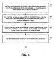
- FIG. 4 is a flowchart illustrating a process 400 implemented by the signal conditioner 300 according to an embodiment of the present invention.
- the operations of the process 400 are described as multiple discrete blocks performed in turn in a manner that is most helpful in understanding embodiments of the invention. However, the order in which they are described should not be construed to imply that these operations are necessarily order dependent or that the operations be performed in the order in which the blocks are presented.
- process 400 is only an example process and other processes may be used to implement embodiments of the present invention.
- a machine-accessible medium with machine-readable instructions thereon may be used to cause a machine (e.g., a processor) to perform the process 400.
- the AGC circuit 304 receives the analog signal 202/203 from the photodetector and the input stage 106 and applies gain or attenuation to the analog signal 202/203 based on the reference amplitude 204.
- the processor 308 provides a gain signal representative of the reference amplitude 204 to the AGC circuit 304, which uses the gain signal as the basis for amplifying or attenuating the analog signal 202/203.
- the MTF detector 310 taps a portion of the analog signal 202/203, detects peak amplitudes of at least one low frequency portion of the analog signal 202/203, and detects peak amplitudes of at least one high frequency portion of the analog signal 202/203.
- the processor 308 selects a new gain signal based on an algorithm that relates the reference amplitude 204, the Gain High signal, and the Gain Low signal, and provides the new gain signal to the AGC circuit 304. In one embodiment, the processor 308 determines that the Gain High signal is disproportionately less than the Gain Low signal and the reference amplitude 204. In this embodiment, the new gain signal can inform the AGC circuit 304 to amplify the analog signal 202/203 regardless of whether such amplification will cause the Gain Low signal to exceed the reference amplitude 204.
- the Gain Low signal is approximately equal to the Gain High signal, but the analog signal 202/203 is less than the reference amplitude 204.
- the new gain signal can inform the AGC circuit 304 to amplify the analog signal 202/203 to bring it within the reference amplitude 204.
- other amplification and attenuation schemes are possible and after reading the description herein a person of ordinary skill in the relevant are will readily recognize how to implement embodiments of the present invention for various combinations of Gain High, Gain Low, and reference amplitude 204 values.
- the AGC circuit 304 uses the new gain signal as a basis for amplifying or attenuating the analog signal 202/203.
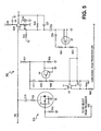
- FIG. 5 is a schematic diagram of the AGC circuit 304 according to an embodiment of the present invention.
- the AGC circuit 308 includes capacitors C4 (0.1 ⁇ F), C10 (0.1 ⁇ F), C15 (39pF), C17 (0.1 ⁇ F), C21 (12pF), C22 (30 ⁇ F), C24 (580pF), and C30 (100pF), operational amplifiers U3A (non-inverting) and U4 (inverting), transistors Q4 (compensation junction field-effect transistor (JFET), and Q7 (gain JFET, acting as a voltage-controlled resistor), resistors R4 (240), R8 (5.1K ⁇ ), R19 (24 ⁇ ), R21 (10K ⁇ ), R24 (24 ⁇ ), R26 (10K ⁇ ), R28 (4.7K ⁇ ), R32 (20K ⁇ ), R35 (100K ⁇ ), R39 (100K ⁇ ), R41 (100K ⁇ ), R43 (100k ⁇ ), R46 (8.2K ⁇ ), and R47 (10K ⁇ ).
- C21 provides a high-frequency compensation filter to roll off noise and provide signal stability for amplifier U3A.
- C22 and R24 provide a low-frequency DC blocking filter to reduce bias voltages for U4 and FET Q7 from interacting to produce inappropriate DC output offset and asymmetry for the analog signal 202/203.
- R19 and C10, R4, and C4 are power supply (e.g., 5 volts) filters for U3A.
- R26 and the equivalent resistance of JFET Q7 determine the gain of U3A.
- JFET Q4 and Q7 are matched transistors.
- R41, R43, and C24 are bias elements for the main gain JFET Q7.
- R35, R39, and C17 are similar bias elements for the regulating JFET Q4.
- R21 and R28 provide similar impedance to Q4 that would be seen by Q7.
- U4 drives the gates of Q7 and Q4 and is controlled with an analog signal from the processor 308.
- R47, R46, and C30 allow gain adjustment for exact desired JFET gate control.
- the gain signals from the processor 308 controls U4.
- U4 buffers the gain signal and drives JFET Q7, and JFET Q4.
- the JFET Q4 is in the positive feedback path of U4.
- U4 Based on the gain signal from the processor 308, U4 outputs the gate voltage to JFET Q7, which responds according to its characteristic curve providing an equivalent resistance.
- U4 also outputs the gate voltage to JFET Q4, which, too, responds in accordance with its characteristic curve and provides a regulating response back to U4.
- the output from the AGC circuit 304 can be linear over a very wide dynamic range (which in turn results in a very wide range of reading distances, e.g., close to the barcode 102 and far away from the barcode 102).
- the AGC circuit 304 implemented according to embodiments of the present invention uses inexpensive matched JFETs to linearize the response to the gain signal input. As a result, the response of the AGC circuit 304 to the gain signal from the processor 308 can be predicted and deterministic.
- the AGC circuit 304 includes JFET Q7 coupled right after R8.
- JFET Q7 drain is coupled to ground, creating a voltage divider between R8 and the equivalent resistance of JFET Q7 that provides the divided voltage onto the positive input of U3A.
- the AGC circuit 304 includes only one JFET Q7 in which its non-linear response (e.g., response curve) is mapped by the processor 308.
- the mapped values are stored (e.g., in a lookup table) and the processor 308 uses the mapped values to generate the same predictive gain adjustment.
- Q4 and Q7 are JFETs
- Q4 and/or Q7 can be any suitable gain element including, but not limited to, bipolar junction transistor (BJT), a MOSFET, vacuum tube, a gallium arsenide (GaAs) FET, a heterojunction bipolar junction transistor (HBJT), and the like.
- BJT bipolar junction transistor
- MOSFET MOSFET
- GaAs gallium arsenide
- HJT heterojunction bipolar junction transistor
- the MTF detector 310 taps a portion of the analog signal 202/203, detects peak amplitudes of at least one frequency portion (e.g., low frequencies) of the analog signal 202/203, and detects peak amplitudes of at least one other frequency portion (e.g., high frequencies) of the analog signal 202/203.
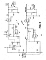
- Figure 6 is a schematic diagram of the MTF detector 310 according to an embodiment of the present invention.
- the MTF detector 310 includes two frequency detection circuits 602 and 604.
- the frequency detection circuit 602 detects higher frequencies within the analog signal 202/203 in the range of approximately a few hundred kilohertz to approximately several hundred kilohertz.
- the frequency detection circuit 604 detects lower frequencies within the analog signal 202/203 in the range of approximately a few tens of kilohertz to approximately a few hundred kilohertz.
- embodiments of the present invention are not limited to detecting only two or only these particular two frequency ranges within analog signals representative of barcodes.
- several and different frequency ranges can be detected and provided to the processor 308 (e.g., one frequency range can be within another frequency range).
- the frequency detection circuit 604 includes capacitors C37 (580pF), C38 (0.1 ⁇ F), C39 (200pF), and C41 (8.2pF), diodes D4, D5, and D6, amplifier U7A, transistor Q8A, and resistors R51 (10K ⁇ ), R52 (100K ⁇ ), R53 (120K ⁇ ), R54 (330 ⁇ ), R55 (1K ⁇ ), R56 (10K ⁇ ), and R57 (1K ⁇ ).
- the tapped analog signal 202/203 enters the frequency detection circuit 604 through C37 and D5.
- C37 and D5 rectify the analog signal 202/203 to ground.
- C37, R51, and R55 provide for signal loading isolation and the low-end cut-off frequency for the frequency detection circuit 604.
- U7A amplifies the analog signal 202/203.
- the combination of U7A, D4, and D6 detects the peak amplitudes in the analog signal 202/203 that fall within the bandwidth of the frequency detection circuit 604.
- C39 and R53 provide a hold time constant and develop a charge based on the peak values of the portions of the analog signal 202/203 that are within the bandwidth of the frequency detection circuit 604.
- the charge on C39 is the Gain Low signal sent to the processor 308.
- the processor 308 provides a signal on the base of Q8A through R54 to clear the charge on C39, and thus reset the Gain Low signal, after a new gain signal has been sent to the AGC circuit 304.
- the frequency detection circuit 602 includes capacitors C43 (68pF), C45 (0.015 ⁇ F), C46 (200pF), and C47 (8.2pF), diodes D7, D8, and D9, amplifier U7B, transistor Q8B, and resistors R58 (10K ⁇ ), R59 (100 ⁇ ), R60 (1K ⁇ ), R61 (200K ⁇ ), R62 (330 ⁇ ), R63 (10K ⁇ ), and R64 (510 ⁇ ).
- the tapped analog signal 202/203 enters the frequency detection circuit 602 through C43 and D7.
- C43 and D7 rectify the analog signal 202/203 to ground.
- C43, R58, and R60 provide for signal loading isolation and the low-end cut-off frequency for the frequency detection circuit 602.
- U7A amplifies the analog signal 202/203.
- C45 and R59 provide an additional low-end cut-off frequency for the frequency detection circuit 602.
- the combination of U7B, D8, and D9 detects the peak amplitudes in the analog signal 202/203 that fall within the bandwidth of the frequency detection circuit 602.
- C46 and R61 provide a hold time constant and develop a charge based on the peak values of the portions of the analog signal 202/203 that are within the bandwidth of the frequency detection circuit 602.
- the charge on C46 is the Gain High signal sent to the processor 308.
- the processor 308 provides a signal on the base of Q8B through R62 to clear the charge on C46, and thus reset the Gain High signal, after a new gain signal has been sent to the AGC circuit 304.
- FIG. 7 is a flowchart illustrating process 700 for implementing the selectable noise filter 312.
- the operations of the process 700 are described as multiple discrete blocks performed in turn in a manner that is most helpful in understanding embodiments of the invention. However, the order in which they are described should not be construed to imply that these operations are necessarily order dependent or that the operations be performed in the order in which the blocks are presented.
- process 700 is only an example process and other processes may be used to implement embodiments of the present invention.
- a machine-accessible medium with machine-readable instructions thereon may be used to cause a machine (e.g., a processor) to perform the process 700.
- a machine e.g., a processor
- a user can manually implement the process 700.
- the processor 308 determines that the Gain Low signal is approximately equal to the Gain High signal.
- the processor 308 applies a new gain signal to the AGC circuit 304, which informs the AGC circuit 304 to amplify/attenuate/maintain the analog signal 202/203 (to bring it to) within the reference amplitude 204.
- the processor 308 determines whether the selectable noise filter 312 is ON or OFF.
- the processor 308 determines whether the read rate for the platform 100 is less than a predetermined value (e.g., less than approximately one hundred percent ( ⁇ 100%)).
- a predetermined value e.g., less than approximately one hundred percent ( ⁇ 100%).
- read rate is defined as the number of successful decodes of the analog signal 202/203 per number of attempted reads (e.g. ten successful decodes out of ten attempted reads is one hundred percent read rate). If the read rate is less than the predetermined value, then the processor 308 turns the selectable noise filter 312 ON.
- the processor 308 determines whether the read rate increased or decreased. If the read rate decreases, then in a block 714, the processor 308 turns the selectable noise filter 312 OFF. If the read rate increases, then in a block 716, the processor 308 permits the selectable noise filter 312 to remain ON.
- the processor 308 determines that the selectable noise filter 312 is ON, then the process 700 passes to the block 712 to determine whether the read rate is increasing or decreasing.
- the processor 308 determines that the read rate is not less than the predetermined value, then the process passes to the block 714 and the processor 308 keeps the selectable noise filter 312 is OFF.
- the noise filter 312 includes resistors R32 and R42, (1K ⁇ ), a capacitor C15, and a metal oxide semiconductor field-effect transistor (MOSFET) Q5.
- R32, R42, C15, and MOSFET Q5 work in combination with existing resistor R8 to form the noise filter 312, which allows a selected range of frequencies within the analog signal 202/203 to pass, while preventing the unwanted paper and noise frequencies from passing.
- the MOSFET Q5 is a switch controlled by the processor 308 to select or deselect the noise filter 312 from the circuitry in the signal conditioner 300.
- R42 is a pull-down resistor.
- R8, C 15, and R32 determine the frequency point and attenuation factor of the filter.
- the selectable noise filter 312 filters out the noise 240 on the analog signal 202/203.
- Q5 can be a JFET switch controlled by the processor 308 to select or deselect the noise filter 312 from the circuitry in the signal conditioner 300.
- Q5 can provide a range of attenuation levels across a range of frequencies as defined by the poles of the noise filter 312.
- Embodiments of the present invention may be implemented using hardware, software, or a combination thereof.
- the software may be stored on a machine-accessible medium.
- a machine-accessible medium includes any mechanism that provides (i.e., stores and/or transmits) information in a form accessible by a machine (e.g., a computer, network device, personal digital assistant, manufacturing tool, any device with a set of one or more processors, etc.).
- a machine-accessible medium includes recordable and non-recordable media (e.g., read only memory (ROM), random access memory (RAM), magnetic disk storage media, optical storage media, flash memory devices, etc.), as well as electrical, optical, acoustic, or other form of propagated signals (e.g., carrier waves, infrared signals, digital signals, etc.).
Landscapes
- Physics & Mathematics (AREA)
- Engineering & Computer Science (AREA)
- Electromagnetism (AREA)
- Artificial Intelligence (AREA)
- Toxicology (AREA)
- General Health & Medical Sciences (AREA)
- Health & Medical Sciences (AREA)
- Computer Vision & Pattern Recognition (AREA)
- General Physics & Mathematics (AREA)
- Theoretical Computer Science (AREA)
- Control Of Amplification And Gain Control (AREA)
- Amplifiers (AREA)
- Digital Transmission Methods That Use Modulated Carrier Waves (AREA)
- Image Input (AREA)
- Tone Control, Compression And Expansion, Limiting Amplitude (AREA)
Priority Applications (1)
| Application Number | Priority Date | Filing Date | Title |
|---|---|---|---|
| EP09166874.9A EP2112618B1 (en) | 2004-04-16 | 2005-04-04 | Barcode scanner with linear automatic gain control (AGC), modulation transfer function detector, and selectable noise filter |
Applications Claiming Priority (2)
| Application Number | Priority Date | Filing Date | Title |
|---|---|---|---|
| US10/825,944 US7216811B2 (en) | 2004-04-16 | 2004-04-16 | Barcode scanner with linear automatic gain control (AGC), modulation transfer function detector, and selectable noise filter |
| PCT/US2005/011226 WO2005106768A2 (en) | 2004-04-16 | 2005-04-04 | Barcode scanner with linear automatic gain control (agc), modulation transfer function detector, and selectable noise filter |
Related Child Applications (2)
| Application Number | Title | Priority Date | Filing Date |
|---|---|---|---|
| EP09166874.9A Division EP2112618B1 (en) | 2004-04-16 | 2005-04-04 | Barcode scanner with linear automatic gain control (AGC), modulation transfer function detector, and selectable noise filter |
| EP09166874.9A Division-Into EP2112618B1 (en) | 2004-04-16 | 2005-04-04 | Barcode scanner with linear automatic gain control (AGC), modulation transfer function detector, and selectable noise filter |
Publications (3)
| Publication Number | Publication Date |
|---|---|
| EP1741046A2 EP1741046A2 (en) | 2007-01-10 |
| EP1741046A4 EP1741046A4 (en) | 2009-05-27 |
| EP1741046B1 true EP1741046B1 (en) | 2015-05-20 |
Family
ID=35095275
Family Applications (2)
| Application Number | Title | Priority Date | Filing Date |
|---|---|---|---|
| EP20050731262 Expired - Lifetime EP1741046B1 (en) | 2004-04-16 | 2005-04-04 | Barcode scanner with linear automatic gain control (agc), modulation transfer function detector, and selectable noise filter |
| EP09166874.9A Expired - Lifetime EP2112618B1 (en) | 2004-04-16 | 2005-04-04 | Barcode scanner with linear automatic gain control (AGC), modulation transfer function detector, and selectable noise filter |
Family Applications After (1)
| Application Number | Title | Priority Date | Filing Date |
|---|---|---|---|
| EP09166874.9A Expired - Lifetime EP2112618B1 (en) | 2004-04-16 | 2005-04-04 | Barcode scanner with linear automatic gain control (AGC), modulation transfer function detector, and selectable noise filter |
Country Status (6)
| Country | Link |
|---|---|
| US (4) | US7216811B2 (enExample) |
| EP (2) | EP1741046B1 (enExample) |
| JP (2) | JP2007534062A (enExample) |
| KR (2) | KR101107033B1 (enExample) |
| CN (3) | CN101645132B (enExample) |
| WO (1) | WO2005106768A2 (enExample) |
Families Citing this family (16)
| Publication number | Priority date | Publication date | Assignee | Title |
|---|---|---|---|---|
| US7216811B2 (en) * | 2004-04-16 | 2007-05-15 | Microscan Systems Incorporated | Barcode scanner with linear automatic gain control (AGC), modulation transfer function detector, and selectable noise filter |
| US8136721B2 (en) * | 2006-05-12 | 2012-03-20 | International Business Machines Corporation | Enhanced check code line image capture for improved OCR |
| US8820645B2 (en) * | 2007-09-28 | 2014-09-02 | Symbol Technologies, Inc. | Method and system for optimizing system settings of a laser scanner control system |
| WO2009061319A1 (en) * | 2007-11-08 | 2009-05-14 | Optoelectronics Co., Ltd. | Signal processing for light beam sensing |
| US20100219246A1 (en) * | 2007-11-08 | 2010-09-02 | Optoelectronics Co. Ltd. | Signal processing for light beam sensing |
| US8622302B2 (en) | 2009-03-17 | 2014-01-07 | Datalogic ADC, Inc. | Systems and methods for compensating for fixed pattern noise |
| US8950678B2 (en) | 2010-11-17 | 2015-02-10 | Hand Held Products, Inc. | Barcode reader with edge detection enhancement |
| US8983833B2 (en) * | 2011-01-24 | 2015-03-17 | Continental Automotive Systems, Inc. | Method and apparatus for masking wind noise |
| DE102011085833B4 (de) * | 2011-11-07 | 2016-03-31 | Photonic Sense GmbH | Zusammensetzung zur Stabilisierung von Siliziumpartikeln in wässrigen Medien und deren Verwendung |
| US9465967B2 (en) | 2012-11-14 | 2016-10-11 | Hand Held Products, Inc. | Apparatus comprising light sensing assemblies with range assisted gain control |
| TW201531951A (zh) * | 2014-02-07 | 2015-08-16 | Cipherlad Co Ltd | 可動態切換的條碼讀取方法 |
| CN104182714B (zh) * | 2014-08-22 | 2017-05-10 | 深圳市兴通物联科技有限公司 | 校正信号畸变的方法及激光条码扫描平台 |
| US20180018624A1 (en) * | 2016-07-14 | 2018-01-18 | Zebrasci, Inc. | Method of Tracking and Tracing Syringes in the Pharmaceutical Industry |
| TWI609331B (zh) * | 2016-11-22 | 2017-12-21 | 陳叁豪 | 具多重光譜的數位浮水印圖像與其設計方法 |
| CN107066909B (zh) * | 2016-12-29 | 2019-11-12 | 西安中颖电子有限公司 | 一种周期性一维条码信号加强的方法和模块 |
| EP4092913B1 (en) * | 2021-05-18 | 2024-05-15 | Renesas Design Austria GmbH | Transmitter with a frequency measurement stage |
Family Cites Families (42)
| Publication number | Priority date | Publication date | Assignee | Title |
|---|---|---|---|---|
| GB1575098A (en) * | 1977-06-15 | 1980-09-17 | Communications Patents Ltd | Method for measuring crossview between channels in a wired television broadcasting system |
| US4740675A (en) | 1986-04-10 | 1988-04-26 | Hewlett-Packard Company | Digital bar code slot reader with threshold comparison of the differentiated bar code signal |
| JP2581047B2 (ja) * | 1986-10-24 | 1997-02-12 | ヤマハ株式会社 | 楽音信号発生方法 |
| US5705800A (en) * | 1996-03-05 | 1998-01-06 | Symbol Technologies, Inc. | Laser scanner system for controlling the optical scanning of bar codes |
| US4963756A (en) | 1989-10-13 | 1990-10-16 | Hewlett-Packard Company | Focused line identifier for a bar code reader |
| US5140146A (en) | 1989-11-20 | 1992-08-18 | Symbol Technologies, Inc. | Bar code symbol reader with modulation enhancement |
| US5126545A (en) * | 1990-01-16 | 1992-06-30 | Symbol Technologies, Inc. | Portable laser scanning system having a motor drive with no DC windings |
| US5608200A (en) | 1990-09-28 | 1997-03-04 | Symbol Technologies, Inc. | Method of collecting and adjusting bar code data from a laser bar code reader |
| US5270875A (en) * | 1990-11-13 | 1993-12-14 | Colorado Memory Systems, Inc. | Programmable filter/equalizer for duel speed and density magnetic recording devices |
| US5168148A (en) * | 1990-12-28 | 1992-12-01 | Symbol Technologies, Inc. | Automatic gain control circuit |
| US5200597A (en) * | 1991-02-07 | 1993-04-06 | Psc, Inc. | Digitally controlled system for scanning and reading bar codes |
| CA2056272C (en) * | 1991-06-14 | 2001-10-16 | Patrick Salatto, Jr. | Combined range laser scanner |
| US5504318A (en) | 1991-09-13 | 1996-04-02 | Symbol Technologies, Inc. | Analog waveform decoder using peak locations |
| US5734152A (en) | 1995-05-31 | 1998-03-31 | Symbol Technologies, Inc. | Optical scanners and signal processors therefor |
| US5461223A (en) | 1992-10-09 | 1995-10-24 | Eastman Kodak Company | Bar code detecting circuitry |
| US5371361A (en) * | 1993-02-01 | 1994-12-06 | Spectra-Physics Scanning Systems, Inc. | Optical processing system |
| US5602376A (en) * | 1993-05-07 | 1997-02-11 | Psc Inc. | Hand-mounted optical scanner system |
| DE4414449C2 (de) * | 1994-04-26 | 1996-03-14 | Leuze Electronic Gmbh & Co | Optoelektronische Vorrichtung zum Erkennen von Kontrastmarken |
| US5777309A (en) | 1995-10-30 | 1998-07-07 | Intermec Corporation | Method and apparatus for locating and decoding machine-readable symbols |
| US6422467B2 (en) * | 1995-12-18 | 2002-07-23 | Metrologic Instruments, Inc. | Reading system a variable pass-band |
| US6036091A (en) | 1995-12-19 | 2000-03-14 | Webscan, Inc. | Method and apparatus supporting high speed evaluation of bar code indicia |
| US5633488A (en) | 1995-12-19 | 1997-05-27 | Webscan, Inc. | Method and apparatus to enable the high speed evaluation of bar code indicia |
| US5852286A (en) * | 1996-03-20 | 1998-12-22 | Psc, Inc. | Method and apparatus for reducing bandwidth limited noise in bar code scanner |
| US5760403A (en) * | 1996-04-18 | 1998-06-02 | Loral Fairchild Corp. | High modulation transfer function CCD X-ray image sensor apparatus and method |
| US6388768B2 (en) * | 1996-04-22 | 2002-05-14 | Minolta Co., Ltd. | Image forming apparatus which excels in reproducibility of colors, fine lines and gradations even in a copy made from a copied image |
| US5969325A (en) | 1996-06-03 | 1999-10-19 | Accu-Sort Systems, Inc. | High speed image acquisition system and method of processing and decoding barcode symbol |
| JP3774797B2 (ja) * | 1996-08-20 | 2006-05-17 | ぺんてる株式会社 | バ−コ−ドイメ−ジ検出装置 |
| JP4132144B2 (ja) | 1997-07-11 | 2008-08-13 | 株式会社キーエンス | バーコード読取装置 |
| JP3814988B2 (ja) * | 1997-10-27 | 2006-08-30 | 株式会社デンソー | 2次元コード読取装置 |
| US6497366B1 (en) * | 1997-12-31 | 2002-12-24 | Ncr Corporation | Methods and apparatus for dual channel video recovery in bar code scanners |
| JP2000163504A (ja) * | 1998-11-27 | 2000-06-16 | Olympus Optical Co Ltd | シンボル情報読み取り装置 |
| JP4085532B2 (ja) * | 1999-08-23 | 2008-05-14 | 株式会社デンソー | バーコード読取装置 |
| US6502751B1 (en) * | 2000-04-26 | 2003-01-07 | Ncr Corporation | Methods and apparatus for dual thresholding in processing of barcode signals |
| ATE431950T1 (de) * | 2000-12-21 | 2009-06-15 | Datalogic Spa | Verfahren und vorrichtung zur fokussierung eines elektrischen signals, welches einen optischen kode repräsentiert |
| CN2461080Y (zh) * | 2001-01-15 | 2001-11-21 | 吴美燕 | 激光条码扫描机的讯号处理装置 |
| ATE378619T1 (de) * | 2002-02-27 | 2007-11-15 | Cdm Optics Inc | Optimierte bildverarbeitung für wellenfrontkodierte abbildungssysteme |
| JP2003308476A (ja) * | 2002-04-12 | 2003-10-31 | Toshiba Corp | バーコード読み取り装置 |
| US20030215791A1 (en) * | 2002-05-20 | 2003-11-20 | Applied Spectral Imaging Ltd. | Method of and system for multiplexed analysis by spectral imaging |
| JP3999055B2 (ja) * | 2002-06-10 | 2007-10-31 | 株式会社オプトエレクトロニクス | 信号検出処理回路 |
| US7260251B2 (en) | 2003-03-31 | 2007-08-21 | Cdm Optics, Inc. | Systems and methods for minimizing aberrating effects in imaging systems |
| US7216811B2 (en) | 2004-04-16 | 2007-05-15 | Microscan Systems Incorporated | Barcode scanner with linear automatic gain control (AGC), modulation transfer function detector, and selectable noise filter |
| US7291856B2 (en) * | 2005-04-28 | 2007-11-06 | Honeywell International Inc. | Sensor and methods for measuring select components in moving sheet products |
-
2004
- 2004-04-16 US US10/825,944 patent/US7216811B2/en not_active Expired - Lifetime
-
2005
- 2005-04-04 KR KR1020117003681A patent/KR101107033B1/ko not_active Expired - Fee Related
- 2005-04-04 WO PCT/US2005/011226 patent/WO2005106768A2/en not_active Ceased
- 2005-04-04 EP EP20050731262 patent/EP1741046B1/en not_active Expired - Lifetime
- 2005-04-04 JP JP2007508380A patent/JP2007534062A/ja active Pending
- 2005-04-04 CN CN200910149238XA patent/CN101645132B/zh not_active Expired - Fee Related
- 2005-04-04 CN CN200910149239.4A patent/CN101976327B/zh not_active Expired - Fee Related
- 2005-04-04 EP EP09166874.9A patent/EP2112618B1/en not_active Expired - Lifetime
- 2005-04-04 CN CN2005800191883A patent/CN101124587B/zh not_active Expired - Fee Related
-
2006
- 2006-11-15 KR KR1020067023936A patent/KR101098322B1/ko not_active Expired - Fee Related
-
2007
- 2007-02-22 US US11/709,969 patent/US7743993B2/en active Active
- 2007-02-22 US US11/710,195 patent/US20070170260A1/en not_active Abandoned
- 2007-04-24 US US11/789,758 patent/US7832644B2/en active Active
-
2010
- 2010-07-14 JP JP2010159473A patent/JP2010267293A/ja active Pending
Also Published As
| Publication number | Publication date |
|---|---|
| EP1741046A2 (en) | 2007-01-10 |
| US20070170260A1 (en) | 2007-07-26 |
| KR101098322B1 (ko) | 2011-12-26 |
| EP2112618A2 (en) | 2009-10-28 |
| JP2010267293A (ja) | 2010-11-25 |
| CN101976327B (zh) | 2014-10-15 |
| US20070215707A1 (en) | 2007-09-20 |
| US7832644B2 (en) | 2010-11-16 |
| US20050230480A1 (en) | 2005-10-20 |
| US20070158426A1 (en) | 2007-07-12 |
| CN101124587B (zh) | 2012-03-21 |
| US7743993B2 (en) | 2010-06-29 |
| CN101645132B (zh) | 2013-04-24 |
| KR101107033B1 (ko) | 2012-01-25 |
| EP2112618B1 (en) | 2015-04-01 |
| JP2007534062A (ja) | 2007-11-22 |
| CN101645132A (zh) | 2010-02-10 |
| KR20110026526A (ko) | 2011-03-15 |
| WO2005106768A2 (en) | 2005-11-10 |
| WO2005106768A3 (en) | 2007-04-19 |
| EP1741046A4 (en) | 2009-05-27 |
| CN101124587A (zh) | 2008-02-13 |
| EP2112618A3 (en) | 2011-08-24 |
| US7216811B2 (en) | 2007-05-15 |
| CN101976327A (zh) | 2011-02-16 |
| KR20070004098A (ko) | 2007-01-05 |
Similar Documents
| Publication | Publication Date | Title |
|---|---|---|
| US7832644B2 (en) | Barcode scanner with linear automatic gain control (AGC), modulation transfer function detector, and selectable noise filter | |
| US5461223A (en) | Bar code detecting circuitry | |
| US5600615A (en) | Device and method for automatically controlling a servo loop gain | |
| CN100483441C (zh) | 在高强度环境光中具有改善的性能的电光读取器 | |
| KR100206334B1 (ko) | 신호처리를 위한 광디스크의 프리앰프 | |
| US20020039332A1 (en) | Focus servo actuating circuit and optical disk device incorporating same | |
| EP1834279A1 (en) | A barcode scanning system with a compensation circuit | |
| EP1805915A1 (en) | A preamplifier circuit having a variable feedback resistance | |
| US7170847B2 (en) | Means for limiting an output signal of an amplifier stage | |
| JPH1196578A (ja) | 光情報検出装置 | |
| JP3341026B2 (ja) | バーコード読み取り装置 | |
| JP3863952B2 (ja) | 外乱光補正機能を有するシンボル情報読み取り装置 | |
| EP1130532A2 (en) | Adaptive audible alert control in a data reader | |
| KR20060123268A (ko) | 광학 디스크로부터 판독한 데이터 신호의 레벨을 제어하기위한 방법 및 시스템 | |
| JP2008192260A (ja) | 光検出装置 | |
| JPS62280979A (ja) | バ−コ−ド検出装置 | |
| JPH03150685A (ja) | 定置式バーコードスキャナ | |
| JPH01260670A (ja) | 自動利得調整回路 |
Legal Events
| Date | Code | Title | Description |
|---|---|---|---|
| PUAI | Public reference made under article 153(3) epc to a published international application that has entered the european phase |
Free format text: ORIGINAL CODE: 0009012 |
|
| 17P | Request for examination filed |
Effective date: 20061116 |
|
| AK | Designated contracting states |
Kind code of ref document: A2 Designated state(s): AT BE BG CH CY CZ DE DK EE ES FI FR GB GR HU IE IS IT LI LT LU MC NL PL PT RO SE SI SK TR |
|
| AX | Request for extension of the european patent |
Extension state: AL BA HR LV MK YU |
|
| PUAK | Availability of information related to the publication of the international search report |
Free format text: ORIGINAL CODE: 0009015 |
|
| DAX | Request for extension of the european patent (deleted) | ||
| A4 | Supplementary search report drawn up and despatched |
Effective date: 20090427 |
|
| 17Q | First examination report despatched |
Effective date: 20110721 |
|
| GRAP | Despatch of communication of intention to grant a patent |
Free format text: ORIGINAL CODE: EPIDOSNIGR1 |
|
| INTG | Intention to grant announced |
Effective date: 20141126 |
|
| GRAS | Grant fee paid |
Free format text: ORIGINAL CODE: EPIDOSNIGR3 |
|
| GRAA | (expected) grant |
Free format text: ORIGINAL CODE: 0009210 |
|
| AK | Designated contracting states |
Kind code of ref document: B1 Designated state(s): AT BE BG CH CY CZ DE DK EE ES FI FR GB GR HU IE IS IT LI LT LU MC NL PL PT RO SE SI SK TR |
|
| REG | Reference to a national code |
Ref country code: GB Ref legal event code: FG4D |
|
| REG | Reference to a national code |
Ref country code: CH Ref legal event code: EP |
|
| REG | Reference to a national code |
Ref country code: AT Ref legal event code: REF Ref document number: 728056 Country of ref document: AT Kind code of ref document: T Effective date: 20150615 |
|
| REG | Reference to a national code |
Ref country code: IE Ref legal event code: FG4D |
|
| REG | Reference to a national code |
Ref country code: DE Ref legal event code: R096 Ref document number: 602005046597 Country of ref document: DE |
|
| REG | Reference to a national code |
Ref country code: AT Ref legal event code: MK05 Ref document number: 728056 Country of ref document: AT Kind code of ref document: T Effective date: 20150520 |
|
| REG | Reference to a national code |
Ref country code: LT Ref legal event code: MG4D |
|
| REG | Reference to a national code |
Ref country code: NL Ref legal event code: MP Effective date: 20150520 |
|
| PG25 | Lapsed in a contracting state [announced via postgrant information from national office to epo] |
Ref country code: FI Free format text: LAPSE BECAUSE OF FAILURE TO SUBMIT A TRANSLATION OF THE DESCRIPTION OR TO PAY THE FEE WITHIN THE PRESCRIBED TIME-LIMIT Effective date: 20150520 Ref country code: ES Free format text: LAPSE BECAUSE OF FAILURE TO SUBMIT A TRANSLATION OF THE DESCRIPTION OR TO PAY THE FEE WITHIN THE PRESCRIBED TIME-LIMIT Effective date: 20150520 Ref country code: LT Free format text: LAPSE BECAUSE OF FAILURE TO SUBMIT A TRANSLATION OF THE DESCRIPTION OR TO PAY THE FEE WITHIN THE PRESCRIBED TIME-LIMIT Effective date: 20150520 Ref country code: PT Free format text: LAPSE BECAUSE OF FAILURE TO SUBMIT A TRANSLATION OF THE DESCRIPTION OR TO PAY THE FEE WITHIN THE PRESCRIBED TIME-LIMIT Effective date: 20150921 |
|
| PG25 | Lapsed in a contracting state [announced via postgrant information from national office to epo] |
Ref country code: GR Free format text: LAPSE BECAUSE OF FAILURE TO SUBMIT A TRANSLATION OF THE DESCRIPTION OR TO PAY THE FEE WITHIN THE PRESCRIBED TIME-LIMIT Effective date: 20150821 Ref country code: AT Free format text: LAPSE BECAUSE OF FAILURE TO SUBMIT A TRANSLATION OF THE DESCRIPTION OR TO PAY THE FEE WITHIN THE PRESCRIBED TIME-LIMIT Effective date: 20150520 Ref country code: IS Free format text: LAPSE BECAUSE OF FAILURE TO SUBMIT A TRANSLATION OF THE DESCRIPTION OR TO PAY THE FEE WITHIN THE PRESCRIBED TIME-LIMIT Effective date: 20150920 Ref country code: BG Free format text: LAPSE BECAUSE OF FAILURE TO SUBMIT A TRANSLATION OF THE DESCRIPTION OR TO PAY THE FEE WITHIN THE PRESCRIBED TIME-LIMIT Effective date: 20150820 |
|
| PG25 | Lapsed in a contracting state [announced via postgrant information from national office to epo] |
Ref country code: EE Free format text: LAPSE BECAUSE OF FAILURE TO SUBMIT A TRANSLATION OF THE DESCRIPTION OR TO PAY THE FEE WITHIN THE PRESCRIBED TIME-LIMIT Effective date: 20150520 Ref country code: DK Free format text: LAPSE BECAUSE OF FAILURE TO SUBMIT A TRANSLATION OF THE DESCRIPTION OR TO PAY THE FEE WITHIN THE PRESCRIBED TIME-LIMIT Effective date: 20150520 |
|
| REG | Reference to a national code |
Ref country code: DE Ref legal event code: R097 Ref document number: 602005046597 Country of ref document: DE |
|
| PG25 | Lapsed in a contracting state [announced via postgrant information from national office to epo] |
Ref country code: PL Free format text: LAPSE BECAUSE OF FAILURE TO SUBMIT A TRANSLATION OF THE DESCRIPTION OR TO PAY THE FEE WITHIN THE PRESCRIBED TIME-LIMIT Effective date: 20150520 Ref country code: SK Free format text: LAPSE BECAUSE OF FAILURE TO SUBMIT A TRANSLATION OF THE DESCRIPTION OR TO PAY THE FEE WITHIN THE PRESCRIBED TIME-LIMIT Effective date: 20150520 Ref country code: RO Free format text: LAPSE BECAUSE OF NON-PAYMENT OF DUE FEES Effective date: 20150520 Ref country code: CZ Free format text: LAPSE BECAUSE OF FAILURE TO SUBMIT A TRANSLATION OF THE DESCRIPTION OR TO PAY THE FEE WITHIN THE PRESCRIBED TIME-LIMIT Effective date: 20150520 |
|
| PLBE | No opposition filed within time limit |
Free format text: ORIGINAL CODE: 0009261 |
|
| STAA | Information on the status of an ep patent application or granted ep patent |
Free format text: STATUS: NO OPPOSITION FILED WITHIN TIME LIMIT |
|
| 26N | No opposition filed |
Effective date: 20160223 |
|
| REG | Reference to a national code |
Ref country code: DE Ref legal event code: R082 Ref document number: 602005046597 Country of ref document: DE Representative=s name: HERNANDEZ, YORCK, DIPL.-ING., DE |
|
| PG25 | Lapsed in a contracting state [announced via postgrant information from national office to epo] |
Ref country code: SI Free format text: LAPSE BECAUSE OF FAILURE TO SUBMIT A TRANSLATION OF THE DESCRIPTION OR TO PAY THE FEE WITHIN THE PRESCRIBED TIME-LIMIT Effective date: 20150520 |
|
| PG25 | Lapsed in a contracting state [announced via postgrant information from national office to epo] |
Ref country code: BE Free format text: LAPSE BECAUSE OF FAILURE TO SUBMIT A TRANSLATION OF THE DESCRIPTION OR TO PAY THE FEE WITHIN THE PRESCRIBED TIME-LIMIT Effective date: 20150520 |
|
| REG | Reference to a national code |
Ref country code: DE Ref legal event code: R119 Ref document number: 602005046597 Country of ref document: DE |
|
| REG | Reference to a national code |
Ref country code: CH Ref legal event code: PL |
|
| GBPC | Gb: european patent ceased through non-payment of renewal fee |
Effective date: 20160404 |
|
| PG25 | Lapsed in a contracting state [announced via postgrant information from national office to epo] |
Ref country code: LU Free format text: LAPSE BECAUSE OF FAILURE TO SUBMIT A TRANSLATION OF THE DESCRIPTION OR TO PAY THE FEE WITHIN THE PRESCRIBED TIME-LIMIT Effective date: 20160404 |
|
| REG | Reference to a national code |
Ref country code: IE Ref legal event code: MM4A |
|
| REG | Reference to a national code |
Ref country code: FR Ref legal event code: ST Effective date: 20161230 |
|
| PG25 | Lapsed in a contracting state [announced via postgrant information from national office to epo] |
Ref country code: FR Free format text: LAPSE BECAUSE OF NON-PAYMENT OF DUE FEES Effective date: 20160502 Ref country code: DE Free format text: LAPSE BECAUSE OF NON-PAYMENT OF DUE FEES Effective date: 20161101 Ref country code: CH Free format text: LAPSE BECAUSE OF NON-PAYMENT OF DUE FEES Effective date: 20160430 Ref country code: GB Free format text: LAPSE BECAUSE OF NON-PAYMENT OF DUE FEES Effective date: 20160404 Ref country code: LI Free format text: LAPSE BECAUSE OF NON-PAYMENT OF DUE FEES Effective date: 20160430 |
|
| PG25 | Lapsed in a contracting state [announced via postgrant information from national office to epo] |
Ref country code: IE Free format text: LAPSE BECAUSE OF NON-PAYMENT OF DUE FEES Effective date: 20160404 |
|
| PG25 | Lapsed in a contracting state [announced via postgrant information from national office to epo] |
Ref country code: SE Free format text: LAPSE BECAUSE OF FAILURE TO SUBMIT A TRANSLATION OF THE DESCRIPTION OR TO PAY THE FEE WITHIN THE PRESCRIBED TIME-LIMIT Effective date: 20150520 Ref country code: NL Free format text: LAPSE BECAUSE OF FAILURE TO SUBMIT A TRANSLATION OF THE DESCRIPTION OR TO PAY THE FEE WITHIN THE PRESCRIBED TIME-LIMIT Effective date: 20150520 Ref country code: IT Free format text: LAPSE BECAUSE OF NON-PAYMENT OF DUE FEES Effective date: 20160404 |
|
| PG25 | Lapsed in a contracting state [announced via postgrant information from national office to epo] |
Ref country code: CY Free format text: LAPSE BECAUSE OF FAILURE TO SUBMIT A TRANSLATION OF THE DESCRIPTION OR TO PAY THE FEE WITHIN THE PRESCRIBED TIME-LIMIT Effective date: 20150520 Ref country code: HU Free format text: LAPSE BECAUSE OF FAILURE TO SUBMIT A TRANSLATION OF THE DESCRIPTION OR TO PAY THE FEE WITHIN THE PRESCRIBED TIME-LIMIT; INVALID AB INITIO Effective date: 20050404 |
|
| PG25 | Lapsed in a contracting state [announced via postgrant information from national office to epo] |
Ref country code: MC Free format text: LAPSE BECAUSE OF FAILURE TO SUBMIT A TRANSLATION OF THE DESCRIPTION OR TO PAY THE FEE WITHIN THE PRESCRIBED TIME-LIMIT Effective date: 20150520 Ref country code: TR Free format text: LAPSE BECAUSE OF FAILURE TO SUBMIT A TRANSLATION OF THE DESCRIPTION OR TO PAY THE FEE WITHIN THE PRESCRIBED TIME-LIMIT Effective date: 20150520 |