EP1732064A2 - Magnetische Aufzeichnungsköpfe mit Auflageflächenschutz und Herstellungsverfahren dafür - Google Patents
Magnetische Aufzeichnungsköpfe mit Auflageflächenschutz und Herstellungsverfahren dafür Download PDFInfo
- Publication number
- EP1732064A2 EP1732064A2 EP06252605A EP06252605A EP1732064A2 EP 1732064 A2 EP1732064 A2 EP 1732064A2 EP 06252605 A EP06252605 A EP 06252605A EP 06252605 A EP06252605 A EP 06252605A EP 1732064 A2 EP1732064 A2 EP 1732064A2
- Authority
- EP
- European Patent Office
- Prior art keywords
- magnetoresistive
- bearing surface
- layer
- sensor
- monitoring device
- Prior art date
- Legal status (The legal status is an assumption and is not a legal conclusion. Google has not performed a legal analysis and makes no representation as to the accuracy of the status listed.)
- Withdrawn
Links
Images


Classifications
-
- G—PHYSICS
- G11—INFORMATION STORAGE
- G11B—INFORMATION STORAGE BASED ON RELATIVE MOVEMENT BETWEEN RECORD CARRIER AND TRANSDUCER
- G11B5/00—Recording by magnetisation or demagnetisation of a record carrier; Reproducing by magnetic means; Record carriers therefor
- G11B5/127—Structure or manufacture of heads, e.g. inductive
- G11B5/31—Structure or manufacture of heads, e.g. inductive using thin films
- G11B5/3163—Fabrication methods or processes specially adapted for a particular head structure, e.g. using base layers for electroplating, using functional layers for masking, using energy or particle beams for shaping the structure or modifying the properties of the basic layers
- G11B5/3166—Testing or indicating in relation thereto, e.g. before the fabrication is completed
-
- G—PHYSICS
- G11—INFORMATION STORAGE
- G11B—INFORMATION STORAGE BASED ON RELATIVE MOVEMENT BETWEEN RECORD CARRIER AND TRANSDUCER
- G11B5/00—Recording by magnetisation or demagnetisation of a record carrier; Reproducing by magnetic means; Record carriers therefor
- G11B5/127—Structure or manufacture of heads, e.g. inductive
- G11B5/31—Structure or manufacture of heads, e.g. inductive using thin films
- G11B5/3163—Fabrication methods or processes specially adapted for a particular head structure, e.g. using base layers for electroplating, using functional layers for masking, using energy or particle beams for shaping the structure or modifying the properties of the basic layers
- G11B5/3169—Working or finishing the interfacing surface of heads, e.g. lapping of heads
-
- G—PHYSICS
- G11—INFORMATION STORAGE
- G11B—INFORMATION STORAGE BASED ON RELATIVE MOVEMENT BETWEEN RECORD CARRIER AND TRANSDUCER
- G11B5/00—Recording by magnetisation or demagnetisation of a record carrier; Reproducing by magnetic means; Record carriers therefor
- G11B5/127—Structure or manufacture of heads, e.g. inductive
- G11B5/31—Structure or manufacture of heads, e.g. inductive using thin films
- G11B5/3163—Fabrication methods or processes specially adapted for a particular head structure, e.g. using base layers for electroplating, using functional layers for masking, using energy or particle beams for shaping the structure or modifying the properties of the basic layers
- G11B5/3173—Batch fabrication, i.e. producing a plurality of head structures in one batch
-
- G—PHYSICS
- G11—INFORMATION STORAGE
- G11B—INFORMATION STORAGE BASED ON RELATIVE MOVEMENT BETWEEN RECORD CARRIER AND TRANSDUCER
- G11B5/00—Recording by magnetisation or demagnetisation of a record carrier; Reproducing by magnetic means; Record carriers therefor
- G11B5/127—Structure or manufacture of heads, e.g. inductive
- G11B5/33—Structure or manufacture of flux-sensitive heads, i.e. for reproduction only; Combination of such heads with means for recording or erasing only
- G11B5/39—Structure or manufacture of flux-sensitive heads, i.e. for reproduction only; Combination of such heads with means for recording or erasing only using magneto-resistive devices or effects
- G11B5/3903—Structure or manufacture of flux-sensitive heads, i.e. for reproduction only; Combination of such heads with means for recording or erasing only using magneto-resistive devices or effects using magnetic thin film layers or their effects, the films being part of integrated structures
- G11B5/3906—Details related to the use of magnetic thin film layers or to their effects
- G11B5/3929—Disposition of magnetic thin films not used for directly coupling magnetic flux from the track to the MR film or for shielding
-
- G—PHYSICS
- G11—INFORMATION STORAGE
- G11B—INFORMATION STORAGE BASED ON RELATIVE MOVEMENT BETWEEN RECORD CARRIER AND TRANSDUCER
- G11B5/00—Recording by magnetisation or demagnetisation of a record carrier; Reproducing by magnetic means; Record carriers therefor
- G11B5/40—Protective measures on heads, e.g. against excessive temperature
Definitions
- the present invention relates generally to magnetic read and/or write heads and methods of manufacture, and more particularly to magnetoresistive sensors or devices having bearing surface protections and methods of lapping the devices using a reference and monitoring device, and methods of producing high precision stripe height and improved thickness control of the second read gap in magnetoresistive devices.
- Magnetic storage tape continues to be an efficient and effective medium for data storage in computer systems. Increased data storage capacity and retrieval performance is desired of all commercially viable mass storage devices and media.
- linear tape recording a popular trend is toward multi-bump, multi-channel fixed head structures with narrowed recording gaps and data track widths so that many linear data tracks may be achieved on a tape medium of a predetermined width, such as one-half inch width tape.
- data transducer elements e.g., magnetoresistive (MR) elements or devices, on the head and data tracks on the tape are arranged with greater density.
- Magnetic tape heads typically include an active device region including raised strips or ridges, commonly referred to as islands, bumps, or rails, that provide a raised tape support or wear surface across which the magnetic tape advances.
- the embedded transducers can be either a recording device for writing information to a magnetic tape or a reproducing device for reading information from a magnetic tape.
- An embedded recording device produces a magnetic field in the vicinity of a small gap in the core of the device, which causes information to be stored on a magnetic tape as the tape advances across the support surface.
- a reproducing device detects a magnetic field from the surface of a magnetic tape as the tape advances over the support surface.
- raised islands may be included without transducers to help support and guide the magnetic tape over the head, generally referred to as outriggers.
- a plurality of embedded transducers are spaced transversely across a direction of tape transport.
- the transducers may be sized and disposed along an island for varying storage tape data formats, e.g., different numbers of channels, track widths, and track densities.
- a four channel head includes four read and four write transducers spaced transversely across a tape path.
- the width of the read/write transducers and the distance between adjacent read/write transducers are associated with the density of tracks to be written to and read from the storage tape. Storage capacity of magnetic tapes is generally increased with the use of smaller more closely positioned read/write transducers in the tape head.
- the tape head and media designs continue to make changes from one generation to the next. For instance, new data formats with more densely positioned read/write transducer elements on tape heads, more densely positioned tracks on the storage tape, and thinner storage tape increases the storage capacity of storage tape devices.
- the storage tape may be thinned, e.g., lower magnetization thickness (Mrt), while narrowing and thinning the MR sensors in the head.
- Mrt magnetization thickness
- Typical MR sensors for use with magnetic recording heads are manufactured using standard semiconductor type processing methods. For example, multiple rows of magnetic recording transducers are deposited simultaneously on wafer substrates and cut into active device regions for incorporation into a magnetic recording head. After a section of magnetic recording transducers are cut from the wafer, they are subject to a lapping process to reduce the stripe heights of the MR sensors to a desired height and smooth or polish the surface of the structure.
- Stripe height is one of the key parameters that control the signal output and device behavior of a magnetoresistive recording head. The stripe height generally determines the sensitivity of the magnetoresistive device to a magnetic field, where a reduction in stripe height typically produces a more sensitive magnetoresistive device.
- scaled down MR sensors e.g., anisotropic magnetoresistive (AMR), giant magnetoresistive (GMR), or tunneling giant magnetoresistive (TGMR) devices, are used to achieve adequate signal output.
- AMR anisotropic magnetoresistive
- GMR
- ELGs Electronic Lapping Guides
- a pair of ELGs is disposed at each end of a cluster of MR sensors.
- the ELGs are monitored during manufacturing to determine the stripe height of the active MR sensors of the cluster.
- the lapping process is controlled to cease when the ELG resistance reaches a calculated value associated with a desired stripe height of the MR sensors.
- the calculated ELG resistance is subjected to variations in the geometry and material thickness of the ELG devices, which may result in large cluster-to-cluster stripe height variations.
- MR sensors and in particular, GMR and TGMR sensors exposed on the head surface
- ABS air bearing surface
- TBS tape bearing surface
- Disk drive heads which operate in an environment sealed at the factory in clean room conditions, are less susceptible to corrosion than tape drive heads, which must operate while exposed to an often quite harsh ambient atmosphere.
- the ABS of the disk drive head is coated with a thin protective film, which is hard and wear resistant on the air bearing surface of a disk drive head.
- a read head having one or more magnetoresistive (MR) sensors includes an MR sensor and an insulator layer disposed at the same level as the MR sensor.
- the read head further includes a bearing surface, wherein the insulator layer forms a portion of the bearing surface and is disposed between a surface of the MR sensor and the bearing surface to provide protection for the MR sensor from exposure to the bearing surface.
- the MR sensor may include a stack of thin-film layers forming a giant magnetoresistive sensor element, a tunneling giant magnetoresistive sensor element, or an anisotropic magnetoresistive sensor element.
- the stack may further include a slanted surface portion, wherein the insulator layer is disposed on the slanted surface portion, thereby recessing the MR sensor from the bearing surface.
- a read head includes a plurality of MR devices and a pair of electronic lapping guides including a monitoring device and a reference device, wherein the monitoring device and the reference device are used during a material removal process (e.g., mechanical lapping) to form the bearing surface at a desired distance from the MR sensor.
- a material removal process e.g., mechanical lapping
- a method for manufacturing a magnetoresistive sensor includes forming a thin-film stack over a read gap layer, the thin-film stack forming the MR sensor. A portion of the thin-film stack is then removed to define a stripe height of the MR sensor and form a slanted surface. An insulating layer is disposed at the same level as the thin-film stack to protect the exposed elements on the slanted surface from corrosions by the chemicals used during a subsequent liftoff operation and to provide a planar surface for the subsequent high precision photolithographic steps. The structure is then lapped to form a bearing surface adjacent the slanted surface of the MR sensor. In particular, the structure is lapped such that the insulating material is disposed between the slanted surface of the thin-film stack and the bearing surface.
- a method includes eliminating or minimizing oxide encroachment into the active device region so that a precisely targeted and uniform second read gap layer is formed over the MR sensor and asymmetry control is maintained.
- the Permanent Magnet (PMG) layer is spaced away from the stripe height layer to reduce or eliminate oxide encroachment into the thin-film stack of the MR sensor. As a result, a more uniform second read gap with a targeted thickness may be achieved.
- the method includes forming a plurality of magnetoresistive devices, a reference device, and a monitoring device, where the reference device includes a stripe height less than the monitoring device.
- Material is removed from a bearing surface, e.g., by lapping, thereby reducing the stripe height of the monitoring device.
- a characteristic of the reference device e.g., resistance, voltage, or the like, is compared with a characteristic of the monitoring device, wherein the characteristic of the monitoring device varies as material is removed from the surface. Material may be removed from the surface until the characteristic of the monitoring device and the reference device are substantially equal or within desired tolerances, at which time, the material removal process may be ceased.
- the reference device may be formed with a similar stripe height of the magnetoresistive devices and serve as a proxy for the stripe height of the magnetoresistive devices.
- the reference device may further include a budget or additional stripe height to accommodate a protective layer or material over the magnetoresistive devices, which is intended to remain after the material removal process.
- the reference device and monitoring device may be formed on the same level and through the same processing steps as readers of the magnetoresistive devices, thereby reducing differences with different processing levels and steps.
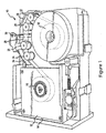
- Figure 1 illustrates an exemplary tape drive system
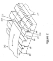
- Figure 2 illustrates an exemplary magnetic recording head including a plurality of MR sensors
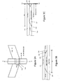
- Figures 3A-3C illustrate top and cross-sectional views of an exemplary wafer defined stripe height MR sensor including a protective layer associated with the MR sensor;
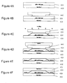
- Figures 4A-4F illustrate an exemplary method for forming MR sensors similar to that illustrated in Figures 3A and 3B ;
- Figure 5A-5C illustrate an exemplary configuration of MR sensors and ELGs (including a monitoring device and reference device) according to one example
- Figure 6 illustrates an exemplary method for manufacturing a magnetic recoding head including a monitoring device and reference device.
- Scaled down MR sensors or elements are desired for higher magnetic recording density.
- the stripe height of the MR sensors is scaled down accordingly.
- Conventional stripe height control using mechanical lapping and calculated Electronic Lapping Guide (ELG) resistance to stop lapping often results in cluster-to-cluster stripe height variations and accuracies on the order of 2,000 ⁇ or greater.
- ELG Electronic Lapping Guide
- exemplary methods described herein may provide improved control over the stripe height of MR sensors, thereby allowing, for example, the manufacture of smaller, more densely positioned MR sensors.
- the stripe height control is on the order of 500 ⁇ or less.
- GMR or TGMR sensors generally include materials on the bearing surface that are prone to corrosions; for example, materials including copper (e.g., copper spacer), cobalt iron (e.g., dusting layer and pinned layer), and IrMn and PtMn (e.g., antiferromagnetic "AFM" layers).
- a hard wear resistant overcoat such as Diamond-Like Carbon (DLC) coating or the like may be used to protect the ABS from corrosion.
- DLC Diamond-Like Carbon
- examples described herein may provide a bearing surface protection in magnetic recording heads to prevent deleterious exposure and corrosion of the device materials. Additionally, in the case of TGMR, the bearing surface protection may prevent or eliminate smearing of the insulator spacer (which could render the device non-functional).
- One exemplary manufacturing method described herein includes depositing an MR layer using semiconductor processing steps to define the stripe height (as opposed to mechanical lapping, for example), where the MR layer further includes a slanted or angled surface portion.
- an ion milling process may be carried out to remove a portion of the MR layer, resulting in a slanted surface of the MR layer adjacent the edge of a photoresist layer.
- a thin insulating layer such as alumina may be deposited after ion milling over the underlying layer and the slanted surface of the MR layer.
- a head may include multiple MR sensors as well as an MR reference device and monitoring device to provide a guide for lapping.
- FIG. 1 illustrates a cut-a-way view of an exemplary magnetic tape drive 10 in which exemplary tape heads and MR sensors as described herein may be used.
- the particular arrangement of tape drive 10 is provided for completeness of the operating environment for exemplary tape heads and to facilitate description of how exemplary tape heads may be utilized during operation of a tape drive.
- Tape drive 10 includes a tape cartridge 12 inserted into a receiver 14.
- Tape drive 10 includes a motor (not shown) which drives a cartridge supply reel 16 and moves tape 20 at a particular speed (e.g., 120 inches per second or more).
- Tape drive 10 may also include a second motor (not shown) which drives a take-up reel 18.
- Tape 20 may be driven in either a forward direction or a reverse direction to write data onto or read data from the tape as controlled by a motor controller circuit (not shown in Figure 1 , but typically provided on one or more printed circuit boards).
- the controller may also be adapted for controlling magnitudes of read/write currents passed through head 30, e.g., to select particular read/write elements for particular data formats and data tracks.
- Tape 20 is guided through tape drive 10 by a plurality of tape guide assemblies 24-29 between the take-up reel 18 and the cartridge 12 and past tape head 30.
- Figure 2 illustrates a perspective view of an exemplary tape head 200 including raised elongated bumps or islands 220, 230, 240, and 250, which may be used in a digital linear tape drive similar to drive 10 of Figure 1 .
- Included along raised islands 220 and 230 are data transducers or MR sensors 224 (shown only along island 220) arranged transversely to the direction of tape transport to enable reading from or writing to tape 202.
- a monitoring device 210 and reference device 211 are included adjacent MR elements 224, which were used during manufacturing tape head 200 as described herein.
- tape head 200 is adapted for contacting media, such as magnetic particle tape 202 that typically has a width ranging from 5 to 20 millimeters.
- exemplary tape heads having MR elements/devices and including (and/or manufactured with) ELGs may be manufactured utilizing any of a number of suitable wafer/semiconductor processing techniques.
- thin-film heads such as head 200 shown in Figure 2
- thin-film heads are fabricated in clean rooms using vacuum or physical vapor deposition methods (such as RF or DC magnetron sputtering, RF or DC diode sputtering, RF or DC triode sputtering) and ion beam deposition, batch photolithographic methods (such as photoresist masking, coating, and developing), chemical assisted and reactive ion-beam etching, photoresist stripping and etching that allow for very small head and element dimensions and precise positioning and alignment of multiple transducer elements (such as MR sensors 224).
- vacuum or physical vapor deposition methods such as RF or DC magnetron sputtering, RF or DC diode sputtering, RF or DC triode sputtering
- each island such as island 220 or 240, may be fabricated by encapsulating layers of materials within two or more substrate materials followed by lapping or fine polishing to achieve a desired media contact contour and surface. Alternatively, each island may be fabricated of several segments or portions that are then epoxy-bonded together to create the elongated islands.
- the media contact surface may be coated with a corrosion or wear resistant layer to protect the read/write elements.
- the resulting active island generally includes the MR sensors, which include a stack of thin layers of different materials (such as metal alloys and insulating materials).
- the tape head may be configured to be a thinfilm inductive head, a thinfilm AMR head, a dual MR head, an integrated thinfilm inductive write and MR or GMR read head, or other thinfilm head design such as TGMR.
- inactive islands or outriggers may be fabricated in a similar fashion to the active islands using similar materials or using different materials. Alternatively, inactive islands may be bonded to the head and formed in differing thinfilm processes.
- Figures 3A-3C illustrate top and cross-sectional views of an exemplary stripe height ("SH") defining layer prior to and after lapping according to one example.
- Figure 3A and 3B illustrate an MR sensor 324 and associated structure prior to lapping
- Figure 3C illustrate the MR sensor 324 and associated structure after mechanical lapping to define a bearing surface.
- the stripe height of the MR sensor 324 is defined by wafer processing steps as more fully described with reference to Figures 4A-4F .
- defining the stripe height with wafer processes e.g., photolithography steps
- MR sensor 324 generally includes a thin-film stack of layers positioned between read gap layers 330 and 331.
- MR sensor 324 may include any of a plurality of MR-type sensors, including, but not limited to, top or bottom spin valve GMR, AMR, synthetic-antiferromagnet (SAF) GMR, spin tunneling, and tunneling junction GMR (TGMR).
- the MR sensor may operate in a current-in-the plane (CIP) mode or current-perpendicular-to-the-plane (CPP) mode.
- CIP current-in-the plane
- CPP current-perpendicular-to-the-plane
- insulating layers such as alumina
- top and bottom layers or magnetic poles of cobaltzirconium-tantalum may be included.
- Poles and shields fabricated using at least one of cobalt, nickel, and iron may also be included.
- the base substrate upon which the MR sensor is layered may be ferrite, aluminum oxide titanium carbide (AlTiC) or other materials.
- MR sensor 324 is further characterized, in part, by a slanted surface 325 at either end of the stripe height (as viewed in the cross-sectional views), where the slanted surface 325 may be defined by a wafer processing step (e.g., a material removal process).
- MR sensor 324 further includes an insulator layer 326 at the same level (e.g., between read gap 330 and read gap 331) as MR sensor 324 and disposed over the slanted surface 325.
- slanted surface 325 may have an angle in the range of 5-30 degrees, but other angles are possible depending on the particular application and processing methods.
- Figure 3C illustrate MR sensor 324 after a mechanical lapping process to define and smooth a bearing surface.
- the mechanical lapping process is performed to define the bearing surface just beyond the edge of the MR sensor 324 and slanted portion 325, such that MR sensor 324 is recessed from (and not exposed to) the bearing surface and protected by a portion of insulator layer 326.
- MR sensor 324 may be recessed at a minimum distance (e.g., at the tip of the slanted region) from the bearing surface by approximately 100-400 ⁇ .
- the minimum recessed distance of the tip of slanted portion 325 is manufactured within a ⁇ 500 ⁇ tolerance, which is achievable, for example, from the use of reference and monitor lapping guides (as discussed in greater detail below).
- Figures 4A-4F illustrate an exemplary method for forming a structure including an MR sensor similar to that shown in Figures 3A-3C .
- an MR layer 424 is deposited on a read gap layer 430 as shown in Figure 4A .
- Read gap layer 430 may include alumina or other suitable material(s).
- MR layer 424 may include a multilayer "stack" of various individual layers such as a cap layer, pinned layer, spacer layer, free layer, buffer layer, and the like to form an AMR, GMR, or TGMR sensor as is known in the art. Additionally , copending U.S. Patent application serial no.
- a photoresist 440 is patterned over MR layer 424 as shown.
- photoresist 440 includes a T-shaped image reversal or bi-layer photoresist patterned after the deposition of MR layer 424 atop read gap 430. Ion milling (or other suitable material removal or etching process) is performed to remove a portion of MR layer 424 in Figure 4C , thereby defining the stripe height of the MR sensor.
- the stripe height of the final MR sensor is therefore defined by a semiconductor processes (in this example, the photolithography step) and may control the stripe height more accurately and consistently than conventional methods (e.g., mechanical lapping).
- the ion milling further results in a slanted or sloped surface 425 in the MR layer 424 as shown.
- the amount of recession from the bearing surface of the final MR sensor depends, at least in part, on the angle of the sloped surface 425 and various film thicknesses of MR layer 424.
- a typical synthetic bottom spin-valve PtMn GMR stack may include a recession ranging from 750 ⁇ to 2440 ⁇ as the angle of the slope varies from approximately 30 degrees to 10 degrees.
- various other ranges of the slope and recession are possible.
- other methods of removing or depositing materials of MR layer 424 to have a particular stripe height and cross-sectional profile shape, including sloped surface 425, similar to that of Figure 4C are possible and contemplated.
- MR layer 424 may be over etched into read gap layer 430. Etching into read gap layer 430 may provide an in situ re-deposition onto slanted surface 425 after etching and may also increases the amount of recession from the bearing surface. Both of these features may benefit surface protection aspects of the manufactured MR sensor.
- an insulator layer 426 in this example, an alumina layer, is deposited over the read gap layer 430 and slanted surface 425 of MR layer 424.
- Insulator layer 426 may be deposited by any suitable method and is deposited to back-fill the removed portion of MR layer 424 with insulating material such as alumina, silicon dioxide, or other suitable insulating material(s).
- Photoresist 440 is then removed in Figure 4E, followed by deposition of a second read gap layer 431 over MR layer 424 and insulator layer 426 as shown in Figure 4F.
- the T-shaped profile of photoresist 440 allows for a solvent to attack photoresist 440 and liftoff MR layer 424.
- the back-filling insulator layer 426 may further protect exposed elements in MR layer 424 on slanted surface 425 from corrosion by chemicals used in the liftoff process. Insulator layer 426 also provides a planar surface for subsequent high precision photolithographic steps.
- oxide encroachment into MR layer 424 can be eliminated or minimized such that uniform and targeted thickness of second read gap 431 can be achieved and asymmetry control from field imaging effects related to the second read gap maintained.
- asymmetry is related to device performance, and generally a slight negative asymmetry is desired for an AMR device. Accordingly, improved control over the thickness and uniformity of the second read gap 431 may improve final device characteristics.
- the structure shown in Figure 4F may then be cut from the wafer and mechanically lapped to a structure similar to that shown in Figure 3C , where insulator layer 426 protects the MR sensor of MR layer 424 from a bearing surface.
- material may be removed to define a bearing surface such that the material of MR layer 424, forming the MR sensor, is recessed (e.g., from 750 ⁇ to 2440 ⁇ ) from the bearing surface.
- the method of mechanical lapping to define the bearing surface may be assisted with the use of a monitoring device and reference device as described with reference to Figures 5A-5C .
- Similar designs and methods are described, for example, in copending U.S. Patent application serial no. 10/917,782 , entitled “METHODS FOR MANUFACTURING MAGNETIC HEADS WITH REFERENCE AND MONITORING DEVICES,” filed August 13, 2004, the entire content of which is hereby incorporated by reference as if fully set forth herein.
- ELGs are included at both ends of a cluster of MR sensors and are used to balance lapping at the beginning of a lapping process.
- an ELG-Reference device ELG-R
- an ELG-Monitoring device ELG-M
- the stripe height of all the MR sensors and the ELG-R are defined by wafer processes, e.g., as described herein.
- the stripe height of the ELG-M is formed to be greater than the stripe height of the MR sensors and the ELG-R.
- a characteristic, e.g., resistance, of the ELG-M and ELG-R is monitored and lapping ceased when the resistance of ELG-M reaches a predetermined value in relation to ELG-R, e.g., the same value as ELG-R.
- the exemplary lapping process using an ELG-R and ELG-M may provide lapping control within +/- 500 ⁇ accuracy.
- FIGS 5A-5C illustrate top views of an exemplary configuration of active MR sensors 524 and ELGs.
- the ELGs include at least one pair of devices, a monitoring device 510 (ELG-M) and a reference device 511 (ELG-R), located proximate active devices 524, and a large ELG 512 at both ends of the cluster of active devices 524.
- large ELGs 512 are used to balance the initial lapping (or rough lapping) of the structure to level the surface for subsequent lapping processes.
- the reference device 511 and monitoring device 510 may thereafter be used during subsequent lapping to preserve the stripe height of the active devices 524 while leaving a sufficient protection layer, e.g., an insulator material or the like.
- reference device 511 and monitoring device 510 are produced by photolithographic wafer processing similar to active devices 524.
- reference device 511 and monitoring device 510 are formed to have the same or similar structure as active readers except for the wafer defined stripe height of monitoring device 510.
- reference device 511 and monitoring device 510 may be formed on the same level and with the same process steps as readers of active devices 524, thereby reducing or eliminating critical dimension differences associated with different levels.
- reference device 511 and monitoring device 510 may be disposed adjacent or proximate each end of the active device area, for example, at a pitch similar to active devices 524.
- reference device 511 is formed to have a stripe height equal to or greater than the stripe of active devices 524 plus the desired thickness of the insulator material (not shown). In this particular example, a stripe height of 1.0 ⁇ m is shown for illustrative purposes only.
- Monitoring device 510 is formed similarly or identically to active devices 524 and includes an initial stripe height greater than reference device 511 and active devices 524 (in this example, greater than 1.0 ⁇ m).
- reference device 511 is produced with a slightly greater stripe height than the active devices 524 to provide additional budgets for head wear caused by the abrasive tape.
- Measurements of monitoring device 510 and reference device 511 may be compared to determine relative stripe heights, and provide an indication of when to cease lapping. Accordingly, monitoring device 510 may be monitored during lapping and stopped using the wafer-defined reference device 511. Lapping may be controlled to within 0.05 ⁇ m using a monitoring device 510 and reference device 511 as shown in Figures 5A-5C .
- Figure 5C illustrates the exemplary structure post lapping having active devices 524 with wafer defined stripe height and bearing protection features (insulator material not shown).
- the cluster of active devices 524 may be cut from the substrate and incorporated into a head structure similar to Figure 2 , for example.
- monitoring device 510 and reference device 511 remain with active devices 524 after bar cut.
- reference device 511 and/or monitoring device 510 may be cut from the active device region after processing.
- the trackwidth of monitoring device 510 and reference device 511 are equal to or greater than the active readers of active devices 524. This feature may minimize the impact of gauging capability of instruments used in measuring electrical characteristics of the monitoring device 510 and reference device 511. Readers of active devices 524 generally have relatively narrow read trackwidths which often result in low MR resistance values. For example, gauging sensitivity may by improved utilizing a 100 ohm resistor versus a 20 ohm resistor.
- reference devices and monitoring devices may be utilized to improve device-to-device stripe height uniformity.
- any number of reference devices and monitoring devices may be used for each cluster of active devices.
- the reference and monitoring devices may be disposed or intermixed within the active devices. Further, a greater number of monitoring devices could be used than reference devices, or vice versa.
- Figure 6 illustrates an exemplary lapping method using a reference device and monitoring device as described herein, e.g., as shown in Figures 5A-5C.
- a wafer is processed to form active devices, e.g., read/write MR sensors arranged in one or more clusters as described. Further, at least one pair of ELG devices including a monitoring device and reference device is formed. Additionally, the wafer may be processed to include conventional ELGs, e.g., such as large and/or small ELGs as described above.
- the wafer may be manufactured by any suitable wafer processing methods known in the art.
- the wafer is polished to remove material from the ABS/TBS of the substrate including the active devices and monitoring device(s).
- a polishing process is performed, e.g., a lapping process or the like, to remove material from the bearing surface and reduce the insulator layer formed over the active devices to a desired thickness as described.
- several polishing steps may be used, e.g., a rough polish while monitoring conventional large and/or small ELGs, if present, followed by a fine or smooth polishing to reach a desired bearing surface.
- the reference device and monitoring device are monitored intermittently or continuously during the one or more polishing steps of block 620.
- an electrical characteristic e.g., the resistance, voltage, or the like, of the reference device and monitoring device are measured and compared.
- a test signal is sent through the reference and monitoring device to determine the relative stripe heights. Material is removed from the bearing surface of the substrate until the measured values from the reference device and monitoring device are substantial equal, e.g., until the measured values indicate the stripe heights are equal or within desired tolerances.
- the polishing is ceased in block 640 thereby forming the bearing surface at a desired distance from the active devices.
Landscapes
- Engineering & Computer Science (AREA)
- Manufacturing & Machinery (AREA)
- Magnetic Heads (AREA)
- Hall/Mr Elements (AREA)
Applications Claiming Priority (1)
| Application Number | Priority Date | Filing Date | Title |
|---|---|---|---|
| US11/133,493 US7751154B2 (en) | 2005-05-19 | 2005-05-19 | Magnetic recording heads with bearing surface protections and methods of manufacture |
Publications (2)
| Publication Number | Publication Date |
|---|---|
| EP1732064A2 true EP1732064A2 (de) | 2006-12-13 |
| EP1732064A3 EP1732064A3 (de) | 2008-09-17 |
Family
ID=37188756
Family Applications (1)
| Application Number | Title | Priority Date | Filing Date |
|---|---|---|---|
| EP06252605A Withdrawn EP1732064A3 (de) | 2005-05-19 | 2006-05-18 | Magnetische Aufzeichnungsköpfe mit Auflageflächenschutz und Herstellungsverfahren dafür |
Country Status (3)
| Country | Link |
|---|---|
| US (1) | US7751154B2 (de) |
| EP (1) | EP1732064A3 (de) |
| JP (1) | JP2006323992A (de) |
Cited By (1)
| Publication number | Priority date | Publication date | Assignee | Title |
|---|---|---|---|---|
| US8169754B2 (en) | 2007-12-31 | 2012-05-01 | Hitachi Global Storage Technologies, Netherlands, B.V. | Dedicated noncorrosive smear detector |
Families Citing this family (17)
| Publication number | Priority date | Publication date | Assignee | Title |
|---|---|---|---|---|
| US7290325B2 (en) * | 2004-08-13 | 2007-11-06 | Quantum Corporation | Methods of manufacturing magnetic heads with reference and monitoring devices |
| US7477482B2 (en) * | 2005-04-19 | 2009-01-13 | International Business Machines Corporation | Magnetic recording head |
| JP2009048745A (ja) * | 2007-08-22 | 2009-03-05 | Hitachi Maxell Ltd | リニア記録型磁気ヘッドアセンブリ、およびそれを用いた磁気テープ装置 |
| US8542460B2 (en) * | 2008-03-12 | 2013-09-24 | International Business Machines Corporation | Head for tape drive with transversely varying contour |
| US8861132B2 (en) | 2010-07-06 | 2014-10-14 | International Business Machines Corporation | Low friction tape head and system implementing same |
| US8679733B2 (en) | 2011-01-19 | 2014-03-25 | International Business Machines Corporation | Patterning process for small devices |
| US8373944B2 (en) * | 2011-05-26 | 2013-02-12 | International Business Machines Corporation | Low friction tape head and system implementing same |
| US9042062B2 (en) | 2013-08-27 | 2015-05-26 | HGST Netherlands B.V. | Magnetic sensor with recessed AFM shape enhanced pinning and soft magnetic bias |
| US9001473B1 (en) | 2014-03-21 | 2015-04-07 | HGST Netherlands B.V. | TMR/CPP reader for narrow reader gap application |
| US9299369B1 (en) * | 2014-10-29 | 2016-03-29 | International Business Machines Corporation | Multichannel data storage apparatus having abrasion resistant barrier |
| US9786302B1 (en) | 2016-04-08 | 2017-10-10 | Western Digital Technologies, Inc. | Flux-guided tunneling magnetoresistive (TMR) sensor for magnetic tape with reduced likelihood of electrical shorting |
| US10014022B1 (en) | 2017-01-04 | 2018-07-03 | International Business Machines Corporation | Flexible media burnishing apparatus and method |
| US10109310B2 (en) | 2017-03-23 | 2018-10-23 | International Business Machines Corporation | Tape head having sub-ambient channel and methods of manufacture |
| US10699741B1 (en) | 2019-01-08 | 2020-06-30 | International Business Machines Corporation | Multi-channel magnetic recording head having compliantly encapsulated transducers |
| US10803889B2 (en) | 2019-02-21 | 2020-10-13 | International Business Machines Corporation | Apparatus with data reader sensors more recessed than servo reader sensor |
| US11074930B1 (en) | 2020-05-11 | 2021-07-27 | International Business Machines Corporation | Read transducer structure having an embedded wear layer between thin and thick shield portions |
| US11114117B1 (en) | 2020-05-20 | 2021-09-07 | International Business Machines Corporation | Process for manufacturing magnetic head having a servo read transducer structure with dielectric gap liner and a data read transducer structure with an embedded wear layer between thin and thick shield portions |
Family Cites Families (68)
| Publication number | Priority date | Publication date | Assignee | Title |
|---|---|---|---|---|
| US4130847A (en) * | 1977-03-31 | 1978-12-19 | International Business Machines Corporation | Corrosion resistant thin film head assembly and method for making |
| GB2169434B (en) | 1984-11-24 | 1989-09-20 | Magnetic Components Limited | Magnetoresistive sensors |
| JPS6275924A (ja) | 1985-09-27 | 1987-04-07 | Matsushita Electric Ind Co Ltd | 一体化薄膜磁気ヘツド |
| NL9100155A (nl) | 1991-01-30 | 1992-08-17 | Philips Nv | Magneetkop, alsmede werkwijze voor het vervaardigen van een dergelijke magneetkop. |
| NL9100191A (nl) | 1991-02-04 | 1992-09-01 | Philips Nv | Werkwijze voor het vervaardigen van een magneetkop en magneetkop vervaardigd volgens de werkwijze. |
| US5210667A (en) | 1991-02-19 | 1993-05-11 | International Business Machines Corporation | Magnetic recording heads employing multiple lapping guides |
| US5065483A (en) * | 1991-02-19 | 1991-11-19 | International Business Machines Corporation | Method of lapping magnetic recording heads |
| EP0519558B1 (de) | 1991-06-18 | 1996-09-18 | Koninklijke Philips Electronics N.V. | Dünnfilm-Lese-/Schreibkopf ohne Pol-Umgreifeffekt |
| US5241439A (en) | 1991-07-02 | 1993-08-31 | U.S. Philips Corporation | Combined read/write thin film magnetic head with two pairs of flux guides |
| JPH05334629A (ja) | 1992-05-29 | 1993-12-17 | Fujitsu Ltd | 磁気抵抗効果型ヘッド |
| DE4323115A1 (de) | 1992-08-03 | 1994-02-10 | Philips Electronics Nv | Magnetkopf mit einer im wesentlichen Cr¶2¶O¶3¶-haltigen Schicht und Verfahren zum Herstellen eines derartigen Magnetkopfes |
| EP0672303B1 (de) | 1993-10-06 | 1997-12-03 | Koninklijke Philips Electronics N.V. | Magnetoresistive anordnung und diese verwendender magnetkopf |
| JPH07153036A (ja) | 1993-11-30 | 1995-06-16 | Sony Corp | 磁気抵抗効果型磁気ヘッド |
| JP3217625B2 (ja) | 1993-12-22 | 2001-10-09 | ティーディーケイ株式会社 | 磁気抵抗効果型ヘッド |
| US5463805A (en) | 1994-02-07 | 1995-11-07 | Seagate Technology, Inc. | Method of lapping MR. sensors |
| US5544774A (en) | 1994-08-26 | 1996-08-13 | Aiwa Research And Development, Inc. | Method of eliminating pole recession in a thin film magnetic head |
| JPH08153310A (ja) | 1994-11-28 | 1996-06-11 | Sony Corp | 磁気抵抗効果型薄膜磁気ヘッド |
| US5493467A (en) * | 1994-12-27 | 1996-02-20 | International Business Machines Corporation | Yoke spin valve MR read head |
| US5617273A (en) | 1995-06-07 | 1997-04-01 | International Business Machines Corporation | Thin film slider with protruding R/W element formed by chemical-mechanical polishing |
| US5772493A (en) * | 1995-07-31 | 1998-06-30 | Read-Rite Corporation | Method and apparatus for controlling the lapping of magnetic heads |
| US6219205B1 (en) | 1995-10-10 | 2001-04-17 | Read-Rite Corporation | High density giant magnetoresistive transducer with recessed sensor |
| DE69722860T2 (de) * | 1996-01-31 | 2004-05-19 | Koninklijke Philips Electronics N.V. | Magnetkopf mit magnetoresistivem sensor und mit den magnetkopf versehende abtastvorrichtung |
| US5710683A (en) | 1996-04-18 | 1998-01-20 | Storage Technology Corporation | Thin film tape head with substrate for reduced pole-tip recession |
| US5666248A (en) | 1996-09-13 | 1997-09-09 | International Business Machines Corporation | Magnetizations of pinned and free layers of a spin valve sensor set by sense current fields |
| WO1999001778A1 (en) | 1997-07-01 | 1999-01-14 | Koninklijke Philips Electronics N.V. | Magnetic field sensor |
| JPH11120523A (ja) | 1997-10-17 | 1999-04-30 | Akita Prefecture | 磁気抵抗効果型磁気ヘッド |
| US5991119A (en) * | 1997-11-03 | 1999-11-23 | Seagate Technology, Inc. | Proximity head slider having recessed magnetoresistive read transducer |
| US6007731A (en) | 1998-03-23 | 1999-12-28 | Headway Technologies, Inc. | Soft adjacent layer (SAL) magnetoresistive (MR) sensor element with electrically insulated soft adjacent layer (SAL) |
| US6738236B1 (en) | 1998-05-07 | 2004-05-18 | Seagate Technology Llc | Spin valve/GMR sensor using synthetic antiferromagnetic layer pinned by Mn-alloy having a high blocking temperature |
| US6359754B1 (en) * | 1998-07-21 | 2002-03-19 | Seagate Technology Llc | Increased mechanical spacing through localized continuous carbon overcoat |
| WO2000005712A1 (en) | 1998-07-21 | 2000-02-03 | Seagate Technology, Llc. | Reducing sensor temperature in magnetoresistive recording heads |
| JP3439129B2 (ja) * | 1998-08-25 | 2003-08-25 | 富士通株式会社 | 磁気ヘッドの製造方法 |
| US6301084B1 (en) * | 1999-05-21 | 2001-10-09 | International Business Machines Corporation | Protection of second pole tip during fabrication of write head |
| US6193584B1 (en) | 1999-05-27 | 2001-02-27 | Read-Rite Corporation | Apparatus and method of device stripe height control |
| US6347983B1 (en) | 1999-06-09 | 2002-02-19 | Seagate Technology Llc | ELG for both MRE sensor height and resistance monitoring |
| US6433965B1 (en) | 2000-03-02 | 2002-08-13 | Read-Rite Corporation | Laminated carbon-containing overcoats for information storage system transducers |
| TW495745B (en) | 2000-03-09 | 2002-07-21 | Koninkl Philips Electronics Nv | Magnetic field element having a biasing magnetic layer structure |
| US6519124B1 (en) * | 2000-03-27 | 2003-02-11 | Tdk Corporation | Magnetic tunnel junction read head using a hybrid, low-magnetization flux guide |
| JP3462832B2 (ja) * | 2000-04-06 | 2003-11-05 | 株式会社日立製作所 | 磁気抵抗センサ並びにこれを用いた磁気ヘッド及び磁気記録再生装置 |
| US6381106B1 (en) | 2000-04-12 | 2002-04-30 | International Business Machines Corporation | Top spin valve sensor that has a free layer structure with a cobalt iron boron (cofeb) layer |
| DE10196239T1 (de) | 2000-05-25 | 2003-08-07 | Seagate Technology Llc | Verbesserter Lapping-Sensor für Aufzeichnungsköpfe |
| US6504689B1 (en) * | 2000-07-12 | 2003-01-07 | International Business Machines Corporation | Tunnel junction read head with flux guide coupled to and magnetically extending a recessed free layer to an air bearing surface |
| JP3839227B2 (ja) | 2000-07-28 | 2006-11-01 | 株式会社日立グローバルストレージテクノロジーズ | 磁気ヘッド、磁気記録再生装置、磁気記録情報の再生方法及び磁気記録方法 |
| US6669787B2 (en) | 2000-09-18 | 2003-12-30 | Koninklijke Philips Electronics N.V. | Method of manufacturing a spin valve structure |
| JP2002133615A (ja) * | 2000-10-25 | 2002-05-10 | Sony Corp | 磁気抵抗効果型磁気ヘッド |
| JP2002203304A (ja) * | 2000-12-28 | 2002-07-19 | Matsushita Electric Ind Co Ltd | Tmrヘッド |
| JP2002260204A (ja) * | 2001-02-27 | 2002-09-13 | Fujitsu Ltd | 磁気ヘッド |
| JP3823028B2 (ja) | 2001-03-13 | 2006-09-20 | 株式会社日立グローバルストレージテクノロジーズ | 磁気ヘッド |
| US6836392B2 (en) | 2001-04-24 | 2004-12-28 | Hitachi Global Storage Technologies Netherlands, B.V. | Stability-enhancing underlayer for exchange-coupled magnetic structures, magnetoresistive sensors, and magnetic disk drive systems |
| US6680830B2 (en) * | 2001-05-31 | 2004-01-20 | International Business Machines Corporation | Tunnel valve sensor and flux guide with improved flux transfer therebetween |
| US6721139B2 (en) * | 2001-05-31 | 2004-04-13 | International Business Machines Corporation | Tunnel valve sensor with narrow gap flux guide employing a lamination of FeN and NiFeMo |
| US6631055B2 (en) * | 2001-06-08 | 2003-10-07 | International Business Machines Corporation | Tunnel valve flux guide structure formed by oxidation of pinned layer |
| US6724587B2 (en) * | 2001-06-11 | 2004-04-20 | International Business Machines Corporation | Low temperature yoke type tunnel valve sensor |
| JP3563375B2 (ja) * | 2001-06-19 | 2004-09-08 | アルプス電気株式会社 | 磁気検出素子及び前記磁気検出素子を用いた薄膜磁気ヘッド |
| US20030002230A1 (en) | 2001-06-29 | 2003-01-02 | Storage Technology Corporation | Apparatus and method of making a reduced sensitivity spin valve sensor apparatus in which a basic magnetic sensitivity is reduced |
| US20030002232A1 (en) * | 2001-06-29 | 2003-01-02 | Storage Technology Corporation | Apparatus and method of making a reduced sensitivity spin valve sensor apparatus in which a flux carrying capacity is increased |
| US6747852B2 (en) | 2001-08-17 | 2004-06-08 | International Business Machines Corporation | Magnetoresistance sensors with Pt-Mn transverse and longitudinal pinning layers and a decoupling insulation layer |
| JP2003067904A (ja) * | 2001-08-28 | 2003-03-07 | Hitachi Ltd | 磁気抵抗効果型磁気ヘッドおよびその製造方法 |
| US6765770B2 (en) | 2001-10-11 | 2004-07-20 | Storage Technology Corporation | Apparatus and method of making a stabilized MR/GMR spin valve read element using longitudinal ferromagnetic exchange interactions |
| US6757144B2 (en) * | 2002-01-18 | 2004-06-29 | International Business Machines Corporation | Flux guide read head with in stack biased current perpendicular to the planes (CPP) sensor |
| JP3581694B2 (ja) | 2002-03-27 | 2004-10-27 | Tdk株式会社 | 薄膜磁気ヘッドの製造方法 |
| US6684171B2 (en) | 2002-04-22 | 2004-01-27 | International Business Machines Corporation | In-situ stripe height calibration of magneto resistive sensors |
| US7170721B2 (en) * | 2002-06-25 | 2007-01-30 | Quantum Corporation | Method of producing flux guides in magnetic recording heads |
| US6879470B2 (en) * | 2002-08-19 | 2005-04-12 | Quantum Corporation | Thin film recording head with a localized coating to protect against corrosion and electrostatic discharge |
| US6847510B2 (en) * | 2002-09-27 | 2005-01-25 | Hitachi Global Storage Technologies Netherlands B.V. | Magnetic tunnel junction device with bottom free layer and improved underlayer |
| US7161772B2 (en) * | 2003-11-19 | 2007-01-09 | International Business Machines Corporation | Removable ESD protection device using diodes |
| US7061725B2 (en) | 2003-12-01 | 2006-06-13 | Seagate Technology Llc | Magnetic read sensor with stripe width and stripe height control |
| US7290325B2 (en) | 2004-08-13 | 2007-11-06 | Quantum Corporation | Methods of manufacturing magnetic heads with reference and monitoring devices |
-
2005
- 2005-05-19 US US11/133,493 patent/US7751154B2/en active Active
-
2006
- 2006-05-17 JP JP2006137650A patent/JP2006323992A/ja active Pending
- 2006-05-18 EP EP06252605A patent/EP1732064A3/de not_active Withdrawn
Cited By (1)
| Publication number | Priority date | Publication date | Assignee | Title |
|---|---|---|---|---|
| US8169754B2 (en) | 2007-12-31 | 2012-05-01 | Hitachi Global Storage Technologies, Netherlands, B.V. | Dedicated noncorrosive smear detector |
Also Published As
| Publication number | Publication date |
|---|---|
| JP2006323992A (ja) | 2006-11-30 |
| US7751154B2 (en) | 2010-07-06 |
| EP1732064A3 (de) | 2008-09-17 |
| US20060262439A1 (en) | 2006-11-23 |
Similar Documents
| Publication | Publication Date | Title |
|---|---|---|
| US20080013219A1 (en) | Methods of manufacturing magnetic heads with reference and monitoring devices | |
| US10811036B2 (en) | Filled-gap magnetic recording head and method of making | |
| US7751154B2 (en) | Magnetic recording heads with bearing surface protections and methods of manufacture | |
| JP4685734B2 (ja) | 磁気ヘッドスライダの製造方法 | |
| US6879470B2 (en) | Thin film recording head with a localized coating to protect against corrosion and electrostatic discharge | |
| US7898765B2 (en) | Thin-film magnetic head with grooves on medium-opposed surface and manufacturing method of the head | |
| US8065788B2 (en) | Method for manufacturing a slider for a perpendicular magnetic recording head | |
| EP1818915A2 (de) | Magnetoresistiver Kopf und Herstellungsverfahren dafür | |
| US5588199A (en) | Lapping process for a single element magnetoresistive head | |
| US8407882B2 (en) | Method for manufacturing thin film magnetic heads | |
| US20090007416A1 (en) | Method to control mask profile for read sensor definition | |
| US8922954B2 (en) | Data reader with back edge surface | |
| US20070035893A1 (en) | Magnetoresistive sensor having an anisotropic hard bias without a buffer layer | |
| US7211195B2 (en) | Method for providing a liftoff process using a single layer resist and chemical mechanical polishing and sensor formed therewith | |
| US7582218B2 (en) | Method for merging sensor field-mill and electronic lapping guide material placement for a partial mill process and sensor formed according to the method | |
| US7580228B1 (en) | Current perpendicular to plane sensor with non-rectangular sense layer stack | |
| US20070081278A1 (en) | Magnetic head having non-GMR shunt for perpendicular recording and method for making magnetic head having non-GMR shunt for perpendicular recording | |
| US7764466B2 (en) | Thin-film magnetic head with closure and manufacturing method of the head | |
| US7352540B1 (en) | Giant magneto-resistive (GMR) transducer having separation structure separating GMR sensor from head-tape interface | |
| US7474513B1 (en) | Magneto-resistive (MR) transducer having an electrostatic discharge (ESD) element and separation structure in contact with magnetic media | |
| US20040264046A1 (en) | Magnetic head with thinned T-shaped write pole and its fabrication | |
| JP2000020925A (ja) | 磁気抵抗効果型磁気ヘッド | |
| JP2007250118A (ja) | 定盤による面取りを行う磁気ヘッドの製造方法 | |
| JPH11144208A (ja) | 磁気ヘッド |
Legal Events
| Date | Code | Title | Description |
|---|---|---|---|
| PUAI | Public reference made under article 153(3) epc to a published international application that has entered the european phase |
Free format text: ORIGINAL CODE: 0009012 |
|
| AK | Designated contracting states |
Kind code of ref document: A2 Designated state(s): AT BE BG CH CY CZ DE DK EE ES FI FR GB GR HU IE IS IT LI LT LU LV MC NL PL PT RO SE SI SK TR |
|
| AX | Request for extension of the european patent |
Extension state: AL BA HR MK YU |
|
| PUAL | Search report despatched |
Free format text: ORIGINAL CODE: 0009013 |
|
| AK | Designated contracting states |
Kind code of ref document: A3 Designated state(s): AT BE BG CH CY CZ DE DK EE ES FI FR GB GR HU IE IS IT LI LT LU LV MC NL PL PT RO SE SI SK TR |
|
| AX | Request for extension of the european patent |
Extension state: AL BA HR MK YU |
|
| AKX | Designation fees paid |
Designated state(s): DE GB |
|
| STAA | Information on the status of an ep patent application or granted ep patent |
Free format text: STATUS: THE APPLICATION IS DEEMED TO BE WITHDRAWN |
|
| 18D | Application deemed to be withdrawn |
Effective date: 20090318 |