EP1717841A1 - Imagerie de formations de subsurface utilisant un faisceau d' électrons - Google Patents
Imagerie de formations de subsurface utilisant un faisceau d' électrons Download PDFInfo
- Publication number
- EP1717841A1 EP1717841A1 EP06112148A EP06112148A EP1717841A1 EP 1717841 A1 EP1717841 A1 EP 1717841A1 EP 06112148 A EP06112148 A EP 06112148A EP 06112148 A EP06112148 A EP 06112148A EP 1717841 A1 EP1717841 A1 EP 1717841A1
- Authority
- EP
- European Patent Office
- Prior art keywords
- image
- subsurface
- electron beam
- work piece
- feature
- Prior art date
- Legal status (The legal status is an assumption and is not a legal conclusion. Google has not performed a legal analysis and makes no representation as to the accuracy of the status listed.)
- Withdrawn
Links
- 238000010894 electron beam technology Methods 0.000 title claims description 38
- 238000003384 imaging method Methods 0.000 title abstract description 10
- 238000000034 method Methods 0.000 claims abstract description 40
- 239000002184 metal Substances 0.000 claims description 21
- 229910052751 metal Inorganic materials 0.000 claims description 21
- 239000000463 material Substances 0.000 claims description 18
- 238000003801 milling Methods 0.000 claims description 17
- 238000010884 ion-beam technique Methods 0.000 claims description 16
- 239000004065 semiconductor Substances 0.000 claims description 8
- 238000012545 processing Methods 0.000 claims description 4
- 229910052710 silicon Inorganic materials 0.000 claims description 4
- 239000010703 silicon Substances 0.000 claims description 4
- 238000013461 design Methods 0.000 claims description 3
- 239000000758 substrate Substances 0.000 description 13
- 238000013459 approach Methods 0.000 description 8
- 239000002245 particle Substances 0.000 description 8
- 238000011960 computer-aided design Methods 0.000 description 6
- 235000012431 wafers Nutrition 0.000 description 6
- 238000004519 manufacturing process Methods 0.000 description 5
- 230000003287 optical effect Effects 0.000 description 5
- 230000001133 acceleration Effects 0.000 description 4
- 239000000203 mixture Substances 0.000 description 4
- XUIMIQQOPSSXEZ-UHFFFAOYSA-N Silicon Chemical compound [Si] XUIMIQQOPSSXEZ-UHFFFAOYSA-N 0.000 description 3
- 230000002596 correlated effect Effects 0.000 description 3
- 230000000875 corresponding effect Effects 0.000 description 3
- 238000004626 scanning electron microscopy Methods 0.000 description 3
- 239000000126 substance Substances 0.000 description 3
- 230000009977 dual effect Effects 0.000 description 2
- 230000003116 impacting effect Effects 0.000 description 2
- 239000012212 insulator Substances 0.000 description 2
- 150000002500 ions Chemical class 0.000 description 2
- 238000005498 polishing Methods 0.000 description 2
- BLIQUJLAJXRXSG-UHFFFAOYSA-N 1-benzyl-3-(trifluoromethyl)pyrrolidin-1-ium-3-carboxylate Chemical compound C1C(C(=O)O)(C(F)(F)F)CCN1CC1=CC=CC=C1 BLIQUJLAJXRXSG-UHFFFAOYSA-N 0.000 description 1
- 125000003821 2-(trimethylsilyl)ethoxymethyl group Chemical group [H]C([H])([H])[Si](C([H])([H])[H])(C([H])([H])[H])C([H])([H])C(OC([H])([H])[*])([H])[H] 0.000 description 1
- VYPSYNLAJGMNEJ-UHFFFAOYSA-N Silicium dioxide Chemical compound O=[Si]=O VYPSYNLAJGMNEJ-UHFFFAOYSA-N 0.000 description 1
- 230000004075 alteration Effects 0.000 description 1
- 239000002800 charge carrier Substances 0.000 description 1
- 239000004020 conductor Substances 0.000 description 1
- 238000010276 construction Methods 0.000 description 1
- 230000008021 deposition Effects 0.000 description 1
- 238000005516 engineering process Methods 0.000 description 1
- 230000007613 environmental effect Effects 0.000 description 1
- 238000005530 etching Methods 0.000 description 1
- 238000002347 injection Methods 0.000 description 1
- 239000007924 injection Substances 0.000 description 1
- 238000007689 inspection Methods 0.000 description 1
- 150000002739 metals Chemical class 0.000 description 1
- 238000000206 photolithography Methods 0.000 description 1
- 238000000027 scanning ion microscopy Methods 0.000 description 1
- 229910052814 silicon oxide Inorganic materials 0.000 description 1
- 238000006467 substitution reaction Methods 0.000 description 1
- YLJREFDVOIBQDA-UHFFFAOYSA-N tacrine Chemical compound C1=CC=C2C(N)=C(CCCC3)C3=NC2=C1 YLJREFDVOIBQDA-UHFFFAOYSA-N 0.000 description 1
- 229960001685 tacrine Drugs 0.000 description 1
- 238000012876 topography Methods 0.000 description 1
- 238000004627 transmission electron microscopy Methods 0.000 description 1
Images


Classifications
-
- G—PHYSICS
- G01—MEASURING; TESTING
- G01N—INVESTIGATING OR ANALYSING MATERIALS BY DETERMINING THEIR CHEMICAL OR PHYSICAL PROPERTIES
- G01N23/00—Investigating or analysing materials by the use of wave or particle radiation, e.g. X-rays or neutrons, not covered by groups G01N3/00 – G01N17/00, G01N21/00 or G01N22/00
- G01N23/22—Investigating or analysing materials by the use of wave or particle radiation, e.g. X-rays or neutrons, not covered by groups G01N3/00 – G01N17/00, G01N21/00 or G01N22/00 by measuring secondary emission from the material
- G01N23/225—Investigating or analysing materials by the use of wave or particle radiation, e.g. X-rays or neutrons, not covered by groups G01N3/00 – G01N17/00, G01N21/00 or G01N22/00 by measuring secondary emission from the material using electron or ion
- G01N23/2251—Investigating or analysing materials by the use of wave or particle radiation, e.g. X-rays or neutrons, not covered by groups G01N3/00 – G01N17/00, G01N21/00 or G01N22/00 by measuring secondary emission from the material using electron or ion using incident electron beams, e.g. scanning electron microscopy [SEM]
-
- H—ELECTRICITY
- H01—ELECTRIC ELEMENTS
- H01J—ELECTRIC DISCHARGE TUBES OR DISCHARGE LAMPS
- H01J37/00—Discharge tubes with provision for introducing objects or material to be exposed to the discharge, e.g. for the purpose of examination or processing thereof
- H01J37/30—Electron-beam or ion-beam tubes for localised treatment of objects
- H01J37/304—Controlling tubes by information coming from the objects or from the beam, e.g. correction signals
-
- H—ELECTRICITY
- H01—ELECTRIC ELEMENTS
- H01J—ELECTRIC DISCHARGE TUBES OR DISCHARGE LAMPS
- H01J2237/00—Discharge tubes exposing object to beam, e.g. for analysis treatment, etching, imaging
- H01J2237/245—Detection characterised by the variable being measured
- H01J2237/24592—Inspection and quality control of devices
-
- H—ELECTRICITY
- H01—ELECTRIC ELEMENTS
- H01J—ELECTRIC DISCHARGE TUBES OR DISCHARGE LAMPS
- H01J2237/00—Discharge tubes exposing object to beam, e.g. for analysis treatment, etching, imaging
- H01J2237/26—Electron or ion microscopes
- H01J2237/28—Scanning microscopes
- H01J2237/2813—Scanning microscopes characterised by the application
- H01J2237/2817—Pattern inspection
-
- H—ELECTRICITY
- H01—ELECTRIC ELEMENTS
- H01J—ELECTRIC DISCHARGE TUBES OR DISCHARGE LAMPS
- H01J2237/00—Discharge tubes exposing object to beam, e.g. for analysis treatment, etching, imaging
- H01J2237/30—Electron or ion beam tubes for processing objects
- H01J2237/31—Processing objects on a macro-scale
Definitions
- the present invention relates to methods for navigating, including end pointing, using microscopic features that are buried below the surface of a work piece.
- Modern integrated circuits are composed of multiple layers of conductors, insulators, and semiconductors. Many modern integrated circuits are fabricated using "flip chip” technology in which the circuit is mounted upside-down onto a carrier. To inspect or alter interior layers of such circuits after the chip is mounted, it is necessary to approach the circuit from the backside. Semiconductor wafers are typically several hundred microns thick, so it is necessary to remove a substantial amount of material from the backside of the circuit before reaching the circuit. When accessing circuitry from the backside, there are no reference points for navigation, that is, there is no easy way to determine exactly where a particular feature on the circuit is located. Thus, to access the circuitry on a flip chip, one must determine where to remove material to expose the circuit from the backside and when to stop removing material to prevent damage to the circuit. Determining when to stop milling is referred to as "end pointing.”
- Removing the backside material is typically performed in several steps.
- a first step typically includes a process, such as chemical mechanical polishing, that rapidly thins the entire chip, leaving sufficient material to provide mechanical strength for handling the chip.
- a subsequent step involves making a large hole in the material centered on the estimated position of the circuit feature of interest. Such a process is typically done using a laser or an ion beam.
- a process that rapidly removes material is typically not capable of stopping at a precise depth, so as the backside hole approaches the circuit, a second, more accurate process is typically used.
- One method of slowing approaching the circuit from the backside uses ion beam milling along with an "end-pointing" technique that indicates when the feature to be exposed is near or is reached.
- end-pointing technique a light is shown into the hole, and the light induces a current as the hole approaches a transistor region of the circuit. As the optical beam-induced current increases, the user knows that he is getting closer to the transistor region of the circuit.
- Another endpointing technique uses focused ion beam milling to approach an active transistor region of the circuit from the backside. As the ion beam approaches the circuit, it creates charge carriers that cause a leakage current through the transistor. The ion beam is modulated, and a frequency sensitive amplifier amplifies the power supply leakage current at the modulation frequency. When the current achieves a certain level, the user assumes that the ion beam is very close to the active transistor region of the circuit. While this method can tell when a user is getting close to an active transistor region, it does not provide information about where on the surface the ion beam is impacting, other than that it is impacting near an active transistor region.
- One common technique for determining when to stop milling, whether on the backside of a flip chip or on the front side of a conventional circuit, is to observe an image of the circuit when a layer has been milled through.
- an optical microscope can be used to form an image
- the resolution of an optical microscope is on the order of 0.5 ⁇ m, which is insufficient to observe to circuit features, which can be on the order of 0.1 ⁇ m.
- a more appropriate method of observing microscopic devices is by using charged particle beam imaging, such as scanning ion microscopy or scanning electron microscopy.
- a charged particle beam such as a focused ion beam or an electron beam, is scanned across a surface.
- the impact of the charged particle beam causes the ejection of various particles, including secondary electrons, backscattered electrons, and ions.
- the number of particles emitted from each point depends on the composition and the topography at the point.
- An image is formed on a video monitor, with the brightness of each point on the image corresponding to the number of particles emitted from the surface at a corresponding point.
- An image can provide information to navigate by, if the image can be correlated to known information about the circuit.
- the work piece typically is typically supported on a stage.
- the stage can move in three dimensions, "X,” “Y,” and “Z,” and movement of the stage and beam is specified and controlled using system coordinates.
- a work piece typically has its own coordinate system used by its designers to specify where various features are formed.
- By finding registration marks, known as "fiducials,” that are incorporated into the work piece it is possible to correlate work piece coordinates with system coordinates, so that a user can specify a position on the work piece using work piece coordinate, and the system can move the stage and direct the beam, that is "navigate,” to that location. Such correlation is referred to as registration. While milling a chip from the backside, the fiducials are not visible and so it is difficult to register the work piece and to find a desired location.
- imaging techniques are useful for navigating in a plane, such techniques have disadvantages for end pointing.
- the layer can be damaged before the endpoint is determined.
- An object of the invention is to provide a method for subsurface viewing to determine the position of buried microscopic features, for example, to correlate the coordinates of a physical system with the coordinates of an image of the system or with computer design information, or to determine when to stop a milling operation is approaching the buried feature.
- an electron beam having sufficiently high energy to penetrate the surface is directed toward a substrate and an image of subsurface features is formed.
- a user uses the subsurface image to determine the location of the beam impact and to direct the beam to a desired subsurface feature.
- electrons having sufficient energy can penetrate more than a micron into the surface to provide information about subsurface features.
- the subsurface feature can be, for example, an orientation mark, such as a fiducial on an integrated circuit or any feature.
- Viewing the fiducial can allow a user to correlate or register between a map of the substrate, such as computer aided design data of an integrated circuit, with the real surface, so that the use can navigate the beam on the surface to a precise location on the real surface using the map.
- a map of the substrate such as computer aided design data of an integrated circuit
- the subsurface electron beam viewing can also be used for end pointing, that is, for determining when to cease milling.
- Subsurface viewing for alignment is particularly useful for backside navigation in which there is no exposed features to orient on. It is also useful for front side alignment when fiducials or other marks are obscured by a layer.
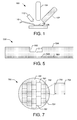
- FIG. 1 shows schematically a dual beam (ion and electron columns) system that can be used to practice a preferred embodiment of the invention.
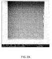
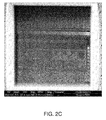
- FIG. 2A-2D shows images formed of a buried metal layers using various electron beam voltages.
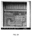
- FIGS. 3A and 3B show images of the buried metal layers of FIGS. 2A-2D obtained at different system parameters.
- FIG. 4 is a flow chart showing a preferred embodiment for use on a semiconductor device.
- FIG. 5 shows a device being operated upon using the steps of FIG. 4.
- FIG. 6 is a flow chart showing a preferred embodiment for correlating system coordinates with work piece coordinates.
- FIG. 7 shows a wafer operated upon by the method shown in FIG. 6.
- FIG. 1 shows schematically a dual beam system 100 that is useful for implementing the present invention.
- One suitable system for example, is the Model Strata 400 available from FEI Company, the assignee of the present application.
- the invention can be practiced using any electron beam system having the capability to produce an electron beam having sufficient beam energy, signal detectors, and resolution required for the specific application.
- an electron beam column 102 and an ion beam column 104 are oriented at an angle to each other, and the beams produced by each column impinge on the same spot 106 on a substrate 108.
- the impact points are separated, and a stage accurately moves the substrate between the beam impact positions.
- the beams can be oriented at an angle to each other to reduce the stage travel distance, or the beams could be parallel.
- the ion beam and electron beam can be coaxial, as described in U.S. Pat. Publication No. 20040108458 .
- a detector 112 detects secondary electrons emitted from the target as it is impacted by the ion beam or the electron beam. Alternatively, a back scatter electron detector, a through-the-lens detector, or other detector could be used.
- system 100 can include many additional features, such as a gas injection system 116 for particle beam deposition or enhanced etching.
- the substrate 108 is typically maintained in a high vacuum, for example, about .001 N/m 2 , although the invention can be practiced in a low vacuum system, such as an environmental scanning electron microscope, as described in U.S. Pat. No. 4,785,182 to Mancuso et al. , which is assigned to the assignee of the present invention.
- a preferred embodiment includes a focused ion beam for altering the work piece, the work piece can also be altered by a laser or by an electron beam using appropriate etch-assisting chemicals, so not all embodiments will include a FIB column.
- An aspect of the invention includes using an electron beam having sufficiently high energy to form a subsurface image, that is, an image of features that are covered by another material.
- Electrons energies used in the invention are typically greater than the energies used in scanning electron microscopy, and less than the energies used in transmission electron microscopy.
- the preferred electron energy will vary with the type of material and the thickness of the covering layer. In various embodiments, electrons having energies greater than about 5 keV, greater than about 10 keV, greater than about 15 keV, greater than about 25 keV, greater than about 30 keV, or greater than about 50 keV may be preferred.
- the invention is not limited to these specific electron energies; lower energies will be useful for thinner layers and greater energies will be useful for thicker layers.
- FIGS. 2A-2D show images created using electrons beams of various energies and a secondary electron detector to observe within a trench created by FIB milling using xenon difluoride as an etch-enhancing gas.
- the substrate shown in FIGS. 2A-2D includes metal lines buried under about 1 ⁇ m to 2 ⁇ m of silicon with about 1 ⁇ m of relatively transparent FIB-deposited silicon oxide over the silicon.
- FIG. 2A in which the electron beam forming the image had an acceleration voltage of 5 kV, does not show any detail of the subsurface metal layer.
- FIG. 2B in which the electron beam forming the image had an acceleration voltage of 15 kV, begins to show some circuit detail on part of the image, probably because the silicon layer is thinner over that portion of the image, or because of electrical charge build up on parts of the circuit under that portion.
- FIG. 2C in which the electron beam forming the image had an acceleration voltage of 20 kV, shows more of the circuit detail is visible.
- FIG. 2D in which the electron beam forming the image had an acceleration voltage of 30 kV, shows sufficient circuit detail to navigate about the surface or to correlated the surface with computer aided design data, an optical map of the surface, or other representation
- FIGS. 3A and 3B show images of the same substrate of FIGS. 2A-2D formed by a 30 kV electron beam, varying the pressure in the sample chamber and the working distance, that is, the distance between the electron lens and the work piece.
- FIG. 3A shows an image taken under a high vacuum, e.g., about .0013 N/m 2 using a working distance of 27.7 mm
- FIG. 3B shows an image taken at a pressure of 93 N/m 2 and a working distance of 4.9 mm.
- FIG. 4 is a flow chart showing a preferred method of correlating design data to a physical surface on a device to enable navigation around the device.
- FIG. 5 shows a device 500 on which the steps of FIG. 4 are performed.
- Device 500 includes buried circuitry including a metal layer 502.
- step 400 device 500 is thinned from the backside 504 by chemical mechanical polishing to a thickness of about 200 microns.
- step 402 an area of interest estimated to contain a desired subsurface feature is located and a 200 ⁇ m by 200 ⁇ m hole 506 about 10-500 ⁇ m deep is milled in the device, the hole centered at a point estimated to contain circuitry of interest.
- step 404 a 1 ⁇ m by 1 ⁇ m hole 512 is milled at the bottom of the 506. Periodically, milling is paused and the bottom of the hole 512 is examined in step 406 using an energy electron beam having sufficient energy in an attempt to view subsurface features.
- the electrons in the beam have energies preferably greater than 15 keV, more preferably greater than 20 keV, even more preferably greater than 25 keV, and most preferably approximately 30 keV or greater, or approximately 50 keV or greater.
- the electron energy used will depend upon how far below the surface the user wants to view and the capabilities of the electron column.
- the electron beam image shows a marked contrast between metal layers, insulating, and semiconducting layers.
- the contrast between different types of semiconductors is not as great. The invention thus facilitates viewing subsurface metals, which are useful for orienting on the substrate.
- the user ceases milling and obtains a subsurface image in step 406 using an electron beam of sufficient energy as described above.
- the electron beam image will typically not show the metal layer as the semiconductor material above the metal layer is too thick to be penetrated by the electron beam.
- the user continues milling in step 412 if the metal layer 502 is not visible. As more material is removed, the user periodically obtains subsurface images, repeating steps 406 to 412. As the bottom of hole 512 approaches metal layer 502, the user will at first begin to see in the subsurface image, a faint view of the metal lines.
- the image of the metal layer 502 becomes much clearer, and, depending upon the electron beam energy, the image of metal lines buried under 1 ⁇ m to 2 ⁇ m of material can be sufficiently clear for a user to determine where on the overall circuit the beam is directed.
- the user can navigate the beam visually to feature 508 in step 420.
- the user can correlate in step 422 the image of the physical circuit to a known map of the circuit to assist in navigating to the position of a desired feature 508 on the circuit in step 420.
- the user can then operate in step 424 on the precise feature or location desired, without damaging other areas in an effort to find the beam location.
- the degree of clarity of the subsurface image also provides information about the depth of the metal layer below the surface, so the user can ensure that milling ceases before the circuit is unintentionally damaged.
- the invention is useful for both navigating in a plane and navigating in three dimensions for endpointing.
- the user uses the subsurface imaging to view buried reference marks to align the physical specimen with a reference image, such as computer aided design data or an optical image taken of a device in a stage of processing when features were exposed.
- a layer is deposited that covers over the fiducials used to align and navigate on the device. While the fiducials are sometimes visible as raised areas in the covering layer, even those signs can be obscured if the surface is "planarized,” that is polished to produce a smooth surface to prepare for the next processing layer.
- FIG. 6 is a flow chart showing the preferred steps of another embodiment of the invention.
- FIG. 7 shows a wafer 700 that includes multiple devices or circuits 702, each circuit including multiple fiducials 704 created on the wafer by the photolithography patterns applied to the wafer to produce the circuit.
- the circuitry and the fiducials have been covered by a material, such as a metal or insulator, that was deposited onto wafer during a previous fabrication step.
- a user navigates to the area that he has estimated includes a first fiducial 704, and directs a relatively high-energy electron beam at low magnification over a broad area to find the fiducial.
- the electron beam energy is "relatively high,” that is, it is typically greater than the energy of an electron beam that is used to image surface features only.
- the user navigates to the area of the fiducial found in step 600.
- the user observes the fiducial at a higher magnification to more precisely determine its position, and the system notes the position of the fiducial on the system coordinates.
- the user can navigate in step 608 to the general area of a second fiducial, and locate the buried fiducial using a relatively high-energy electron beam at low magnification.
- step 610 observes the second fiducial at increased magnification and the system records its coordinates in the system coordinate system.
- the user navigates to a buried third fiducial in step 614, and views the area around the fiducial using a relatively high-energy electron beam at low magnification to locate the fiducial.
- the third fiducial is viewed at increased magnification, and the system notes its coordinates in step 618.
- the location of the fiducials in the system coordinate system are correlated to a work piece coordinate system, such as data from a computer aided design (CAD) database or inspection system, such as another microscope with accurate stage positioning and position readouts that can be used to determine coordinates.
- CAD computer aided design
- the user navigates to any point on the work piece, using the CAD coordinates of the point, which are translated into system coordinates to move the work piece stage and direct the beam.
- the term “navigate” is used herein to include not only determining a position and moving in the X and Y direction on a substrate, but also include determining a vertical position to assist endpointing, that is, to determining when to stop milling as one approaches a buried feature.
- the invention is not limited to use on integrated circuits, but is useful for any multilayer substrate that includes microscopic features covered by another material.
Landscapes
- Chemical & Material Sciences (AREA)
- Analytical Chemistry (AREA)
- Physics & Mathematics (AREA)
- Health & Medical Sciences (AREA)
- Life Sciences & Earth Sciences (AREA)
- Biochemistry (AREA)
- General Health & Medical Sciences (AREA)
- General Physics & Mathematics (AREA)
- Immunology (AREA)
- Pathology (AREA)
- Analysing Materials By The Use Of Radiation (AREA)
- Testing Or Measuring Of Semiconductors Or The Like (AREA)
Applications Claiming Priority (1)
| Application Number | Priority Date | Filing Date | Title |
|---|---|---|---|
| US11/098,578 US7388218B2 (en) | 2005-04-04 | 2005-04-04 | Subsurface imaging using an electron beam |
Publications (1)
| Publication Number | Publication Date |
|---|---|
| EP1717841A1 true EP1717841A1 (fr) | 2006-11-02 |
Family
ID=36609130
Family Applications (1)
| Application Number | Title | Priority Date | Filing Date |
|---|---|---|---|
| EP06112148A Withdrawn EP1717841A1 (fr) | 2005-04-04 | 2006-04-03 | Imagerie de formations de subsurface utilisant un faisceau d' électrons |
Country Status (5)
| Country | Link |
|---|---|
| US (1) | US7388218B2 (fr) |
| EP (1) | EP1717841A1 (fr) |
| JP (1) | JP5719494B2 (fr) |
| CN (1) | CN1855365B (fr) |
| TW (1) | TWI404105B (fr) |
Cited By (1)
| Publication number | Priority date | Publication date | Assignee | Title |
|---|---|---|---|---|
| EP2149897A1 (fr) * | 2008-07-31 | 2010-02-03 | FEI Company | Procédé de broyage et de detection de point d'extremite d'un échantillon |
Families Citing this family (23)
| Publication number | Priority date | Publication date | Assignee | Title |
|---|---|---|---|---|
| US9159527B2 (en) | 2003-10-16 | 2015-10-13 | Carl Zeiss Microscopy, Llc | Systems and methods for a gas field ionization source |
| US8110814B2 (en) | 2003-10-16 | 2012-02-07 | Alis Corporation | Ion sources, systems and methods |
| JP4413746B2 (ja) | 2004-10-28 | 2010-02-10 | 株式会社日立ハイテクノロジーズ | 荷電粒子ビーム装置 |
| WO2007067296A2 (fr) * | 2005-12-02 | 2007-06-14 | Alis Corporation | Sources d'ions, systemes et procedes associes |
| DE102008041815A1 (de) * | 2008-09-04 | 2010-04-15 | Carl Zeiss Nts Gmbh | Verfahren zur Analyse einer Probe |
| CN102812533B (zh) * | 2010-04-07 | 2015-12-02 | Fei公司 | 组合激光器和带电粒子束系统 |
| EP2612342B1 (fr) * | 2010-08-31 | 2018-08-22 | FEI Company | Navigation et traitement d'échantillons à l'aide d'une source d'ions contenant des espèces à masse faible et à masse élevée |
| CN102064077A (zh) * | 2010-12-02 | 2011-05-18 | 北京航空航天大学 | 一种利用同步可控电子束提高聚焦离子束加工精度的方法 |
| CN103403520B (zh) | 2011-01-28 | 2015-12-23 | Fei公司 | Tem样品制备 |
| JP6244307B2 (ja) * | 2011-11-29 | 2017-12-06 | ケーエルエー−テンカー コーポレイション | 表面下欠陥検査用のサンプル作製のためのシステム及び方法 |
| CN103137531B (zh) * | 2011-12-02 | 2016-09-07 | 无锡华润上华科技有限公司 | 晶圆对位方法 |
| JP5986027B2 (ja) * | 2012-03-31 | 2016-09-06 | エフ・イ−・アイ・カンパニー | レーザ・アブレーション中に光学構成部品を保護するシステム |
| US10204762B2 (en) * | 2012-07-16 | 2019-02-12 | Fei Company | Endpointing for focused ion beam processing |
| US8895923B2 (en) * | 2012-11-20 | 2014-11-25 | Dcg Systems, Inc. | System and method for non-contact microscopy for three-dimensional pre-characterization of a sample for fast and non-destructive on sample navigation during nanoprobing |
| CN104122282B (zh) * | 2013-04-24 | 2017-01-18 | 泰科英赛科技有限公司 | 采用聚焦离子束的电路跟踪 |
| JP6490938B2 (ja) * | 2013-10-24 | 2019-03-27 | 株式会社日立ハイテクサイエンス | 断面加工方法、断面加工装置 |
| CN104795302B (zh) | 2013-10-29 | 2018-10-02 | Fei 公司 | 具有用于横切应用的过程自动化的图案识别的差分成像 |
| US9558911B2 (en) | 2014-08-01 | 2017-01-31 | Carl Zeiss Microscopy Gmbh | Method for analyzing and/or processing an object as well as a particle beam device for carrying out the method |
| EP3104155A1 (fr) | 2015-06-09 | 2016-12-14 | FEI Company | Procédé d'analyse de modification de surface d'un échantillon dans un microscope à faisceau de particules chargées |
| US20190287762A1 (en) * | 2018-01-25 | 2019-09-19 | Fei Company | System and method of preparing integrated circuits for backside probing using charged particle beams |
| US12525430B2 (en) * | 2020-04-28 | 2026-01-13 | Hitachi High-Tech Corporation | Charged particle beam apparatus |
| US11280749B1 (en) * | 2020-10-23 | 2022-03-22 | Applied Materials Israel Ltd. | Holes tilt angle measurement using FIB diagonal cut |
| US12288668B2 (en) * | 2023-05-11 | 2025-04-29 | Applied Materials Israel Ltd. | Entropy based image processing for focused ion beam delayer-edge slices detection |
Citations (5)
| Publication number | Priority date | Publication date | Assignee | Title |
|---|---|---|---|---|
| US4683378A (en) * | 1984-07-13 | 1987-07-28 | Hitachi, Ltd. | Apparatus for ion beam work |
| US5594245A (en) * | 1990-10-12 | 1997-01-14 | Hitachi, Ltd. | Scanning electron microscope and method for dimension measuring by using the same |
| EP0863543A2 (fr) * | 1997-03-03 | 1998-09-09 | Schlumberger Technologies, Inc. | Inspection de puces de type Flip-Chip à travers le substrat |
| EP0932022A1 (fr) * | 1998-01-23 | 1999-07-28 | Advantest Corporation | Méthode et appareil pour la mesure de dimensions et l'inspection de structures |
| WO2002025692A1 (fr) * | 2000-09-20 | 2002-03-28 | Fei Company | Controle en temps reel permettant a la fois l'imagerie et l'exposition dans des systemes a faisceau de particule chargee |
Family Cites Families (28)
| Publication number | Priority date | Publication date | Assignee | Title |
|---|---|---|---|---|
| JPH0752293B2 (ja) * | 1987-02-27 | 1995-06-05 | 株式会社日立製作所 | イオンビ−ム加工方法及びその装置 |
| US4785182A (en) * | 1987-05-21 | 1988-11-15 | Electroscan Corporation | Secondary electron detector for use in a gaseous atmosphere |
| JPH0691054B2 (ja) * | 1987-12-24 | 1994-11-14 | 株式会社日立製作所 | イオンビーム加工方法及びその装置 |
| JPH0221549A (ja) * | 1988-07-08 | 1990-01-24 | Jeol Ltd | 走査電子顕微鏡 |
| JP2519512B2 (ja) * | 1988-08-31 | 1996-07-31 | セイコー電子工業株式会社 | 集束イオンビ―ム装置 |
| JPH05290786A (ja) * | 1992-04-10 | 1993-11-05 | Hitachi Ltd | 走査試料像表示方法および装置ならびにそれに供される試料 |
| JP3398403B2 (ja) * | 1992-12-02 | 2003-04-21 | 株式会社日立製作所 | 走査型電子顕微鏡の試料像表示方法 |
| JP3223431B2 (ja) * | 1992-04-09 | 2001-10-29 | 株式会社日立製作所 | 薄膜加工装置 |
| JPH08327514A (ja) * | 1995-06-05 | 1996-12-13 | Nippondenso Co Ltd | 透過電子顕微鏡用試料の作製方法及びその装置 |
| US6885444B2 (en) * | 1998-06-10 | 2005-04-26 | Boxer Cross Inc | Evaluating a multi-layered structure for voids |
| US6262430B1 (en) * | 1998-07-30 | 2001-07-17 | Advanced Micro Devices, Inc. | Integrated system for frontside navigation and access of multi-layer integrated circuits |
| US6344750B1 (en) * | 1999-01-08 | 2002-02-05 | Schlumberger Technologies, Inc. | Voltage contrast method for semiconductor inspection using low voltage particle beam |
| US6252412B1 (en) * | 1999-01-08 | 2001-06-26 | Schlumberger Technologies, Inc. | Method of detecting defects in patterned substrates |
| US6414307B1 (en) * | 1999-07-09 | 2002-07-02 | Fei Company | Method and apparatus for enhancing yield of secondary ions |
| US6452176B1 (en) * | 1999-07-22 | 2002-09-17 | Advanced Micro Devices, Inc. | Arrangement and method for using electron channeling patterns to detect substrate damage |
| US6281025B1 (en) * | 1999-09-30 | 2001-08-28 | Advanced Micro Devices, Inc. | Substrate removal as a function of SIMS analysis |
| JP3749107B2 (ja) * | 1999-11-05 | 2006-02-22 | ファブソリューション株式会社 | 半導体デバイス検査装置 |
| US6322672B1 (en) * | 2000-03-10 | 2001-11-27 | Fei Company | Method and apparatus for milling copper interconnects in a charged particle beam system |
| JP3874996B2 (ja) * | 2000-05-30 | 2007-01-31 | ファブソリューション株式会社 | デバイス検査方法および装置 |
| JP2002072456A (ja) * | 2000-08-30 | 2002-03-12 | Nikon Corp | レチクルリペア方法、それにより得られたレチクル及びレチクルリペア装置 |
| US20020074494A1 (en) * | 2000-12-15 | 2002-06-20 | Lundquist Theodore R. | Precise, in-situ endpoint detection for charged particle beam processing |
| US6548810B2 (en) * | 2001-08-01 | 2003-04-15 | The University Of Chicago | Scanning confocal electron microscope |
| JP2003066118A (ja) * | 2001-08-29 | 2003-03-05 | Sanyo Electric Co Ltd | 半導体装置の故障解析方法 |
| US20030138709A1 (en) * | 2001-11-09 | 2003-07-24 | Burbank Daniel P. | Wafer fabrication having improved laserwise alignment recovery |
| EP1388883B1 (fr) * | 2002-08-07 | 2013-06-05 | Fei Company | Colonne coaxiale FIB-SEM |
| US6787783B2 (en) * | 2002-12-17 | 2004-09-07 | International Business Machines Corporation | Apparatus and techniques for scanning electron beam based chip repair |
| JP2005302600A (ja) * | 2004-04-14 | 2005-10-27 | Seiko Epson Corp | 微細加工方法およびその装置 |
| US20060140144A1 (en) * | 2004-12-27 | 2006-06-29 | Motorola, Inc. | Method and system for providing an open gateway initiative bundle over the air |
-
2005
- 2005-04-04 US US11/098,578 patent/US7388218B2/en not_active Expired - Lifetime
-
2006
- 2006-04-03 CN CN2006100793738A patent/CN1855365B/zh not_active Expired - Fee Related
- 2006-04-03 TW TW095111807A patent/TWI404105B/zh active
- 2006-04-03 EP EP06112148A patent/EP1717841A1/fr not_active Withdrawn
- 2006-04-03 JP JP2006102293A patent/JP5719494B2/ja not_active Expired - Lifetime
Patent Citations (5)
| Publication number | Priority date | Publication date | Assignee | Title |
|---|---|---|---|---|
| US4683378A (en) * | 1984-07-13 | 1987-07-28 | Hitachi, Ltd. | Apparatus for ion beam work |
| US5594245A (en) * | 1990-10-12 | 1997-01-14 | Hitachi, Ltd. | Scanning electron microscope and method for dimension measuring by using the same |
| EP0863543A2 (fr) * | 1997-03-03 | 1998-09-09 | Schlumberger Technologies, Inc. | Inspection de puces de type Flip-Chip à travers le substrat |
| EP0932022A1 (fr) * | 1998-01-23 | 1999-07-28 | Advantest Corporation | Méthode et appareil pour la mesure de dimensions et l'inspection de structures |
| WO2002025692A1 (fr) * | 2000-09-20 | 2002-03-28 | Fei Company | Controle en temps reel permettant a la fois l'imagerie et l'exposition dans des systemes a faisceau de particule chargee |
Cited By (1)
| Publication number | Priority date | Publication date | Assignee | Title |
|---|---|---|---|---|
| EP2149897A1 (fr) * | 2008-07-31 | 2010-02-03 | FEI Company | Procédé de broyage et de detection de point d'extremite d'un échantillon |
Also Published As
| Publication number | Publication date |
|---|---|
| CN1855365A (zh) | 2006-11-01 |
| JP2006284590A (ja) | 2006-10-19 |
| US20060219953A1 (en) | 2006-10-05 |
| US7388218B2 (en) | 2008-06-17 |
| CN1855365B (zh) | 2010-06-09 |
| TWI404105B (zh) | 2013-08-01 |
| TW200723342A (en) | 2007-06-16 |
| JP5719494B2 (ja) | 2015-05-20 |
Similar Documents
| Publication | Publication Date | Title |
|---|---|---|
| US7388218B2 (en) | Subsurface imaging using an electron beam | |
| US11315756B2 (en) | Fiducial design for tilted or glancing mill operations with a charged particle beam | |
| US10529538B2 (en) | Endpointing for focused ion beam processing | |
| US7858936B2 (en) | Slice and view with decoration | |
| EP2904633B1 (fr) | Accès structurel à dimensions multiples | |
| JP5492364B2 (ja) | 3次元基準マーク | |
| US8455822B2 (en) | Navigation and sample processing using an ion source containing both low-mass and high-mass species | |
| US11069509B1 (en) | Method and system for backside planar view lamella preparation | |
| US20190304744A1 (en) | Methods for acquiring planar view stem images of device structures | |
| US10539489B2 (en) | Methods for acquiring planar view STEM images of device structures | |
| KR101275943B1 (ko) | 전자 빔을 이용한 표면 아래 이미징 | |
| US20250290834A1 (en) | Preparation of planar lamella from a multi-layer structure | |
| CN121994844A (zh) | 基于线的终点检测 |
Legal Events
| Date | Code | Title | Description |
|---|---|---|---|
| PUAI | Public reference made under article 153(3) epc to a published international application that has entered the european phase |
Free format text: ORIGINAL CODE: 0009012 |
|
| 17P | Request for examination filed |
Effective date: 20060403 |
|
| AK | Designated contracting states |
Kind code of ref document: A1 Designated state(s): AT BE BG CH CY CZ DE DK EE ES FI FR GB GR HU IE IS IT LI LT LU LV MC NL PL PT RO SE SI SK TR |
|
| AX | Request for extension of the european patent |
Extension state: AL BA HR MK YU |
|
| 17Q | First examination report despatched |
Effective date: 20070131 |
|
| AKX | Designation fees paid |
Designated state(s): DE FR GB |
|
| STAA | Information on the status of an ep patent application or granted ep patent |
Free format text: STATUS: THE APPLICATION IS DEEMED TO BE WITHDRAWN |
|
| 18D | Application deemed to be withdrawn |
Effective date: 20091020 |