EP1715409B1 - Procédé de génération de nombres aléatoires et dispositif à circuit intégré semi-conducteur - Google Patents
Procédé de génération de nombres aléatoires et dispositif à circuit intégré semi-conducteur Download PDFInfo
- Publication number
- EP1715409B1 EP1715409B1 EP04710508A EP04710508A EP1715409B1 EP 1715409 B1 EP1715409 B1 EP 1715409B1 EP 04710508 A EP04710508 A EP 04710508A EP 04710508 A EP04710508 A EP 04710508A EP 1715409 B1 EP1715409 B1 EP 1715409B1
- Authority
- EP
- European Patent Office
- Prior art keywords
- circuit
- random number
- circuits
- signal
- logic
- Prior art date
- Legal status (The legal status is an assumption and is not a legal conclusion. Google has not performed a legal analysis and makes no representation as to the accuracy of the status listed.)
- Expired - Fee Related
Links
Images


Classifications
-
- G—PHYSICS
- G06—COMPUTING; CALCULATING OR COUNTING
- G06F—ELECTRIC DIGITAL DATA PROCESSING
- G06F7/00—Methods or arrangements for processing data by operating upon the order or content of the data handled
- G06F7/58—Random or pseudo-random number generators
-
- G—PHYSICS
- G06—COMPUTING; CALCULATING OR COUNTING
- G06F—ELECTRIC DIGITAL DATA PROCESSING
- G06F7/00—Methods or arrangements for processing data by operating upon the order or content of the data handled
- G06F7/58—Random or pseudo-random number generators
- G06F7/588—Random number generators, i.e. based on natural stochastic processes
-
- G—PHYSICS
- G06—COMPUTING; CALCULATING OR COUNTING
- G06F—ELECTRIC DIGITAL DATA PROCESSING
- G06F7/00—Methods or arrangements for processing data by operating upon the order or content of the data handled
- G06F7/38—Methods or arrangements for performing computations using exclusively denominational number representation, e.g. using binary, ternary, decimal representation
- G06F7/48—Methods or arrangements for performing computations using exclusively denominational number representation, e.g. using binary, ternary, decimal representation using non-contact-making devices, e.g. tube, solid state device; using unspecified devices
- G06F7/57—Arithmetic logic units [ALU], i.e. arrangements or devices for performing two or more of the operations covered by groups G06F7/483 – G06F7/556 or for performing logical operations
-
- G—PHYSICS
- G11—INFORMATION STORAGE
- G11C—STATIC STORES
- G11C7/00—Arrangements for writing information into, or reading information out from, a digital store
- G11C7/06—Sense amplifiers; Associated circuits, e.g. timing or triggering circuits
-
- H—ELECTRICITY
- H04—ELECTRIC COMMUNICATION TECHNIQUE
- H04L—TRANSMISSION OF DIGITAL INFORMATION, e.g. TELEGRAPHIC COMMUNICATION
- H04L9/00—Cryptographic mechanisms or cryptographic arrangements for secret or secure communications; Network security protocols
- H04L9/06—Cryptographic mechanisms or cryptographic arrangements for secret or secure communications; Network security protocols the encryption apparatus using shift registers or memories for block-wise or stream coding, e.g. DES systems or RC4; Hash functions; Pseudorandom sequence generators
Definitions
- the present invention relates to a random number generating method and a semiconductor integrated circuit device and in particular, to a random number generating method appropriate for a semiconductor fabrication technique and a technique which can be effectively used in the semiconductor integrated circuit device.
- the performance of a random number generating circuit may be compared in the quality (irregularity) of the random number, a circuit area, power consumption, response time (time required for generating a new random number), and the like.
- the conventional random number generating circuits have good and bad points.
- True random number has advantages of eventuality, unreproducibility, and unpredictability but it requires a complicated circuit and element which cannot be obtained in a simple device.
- the technique suggested in the first prior art relates to a true random number generating circuit which requires modification or a process (etching process) and its control.
- the second prior art uses a phenomenon occurring in the transient state when power is turned ON. Accordingly, a factor lowering the irregularity of a random number cannot be predicted at the design stage and it is difficult to guarantee the quality of the random number.
- US 2004/006580 A1 discloses a method and circuit for generating a random bit stream based on the thermal noise of a CMOS device.
- JP 2003/332452 A generally suggests to utilise the dispersion of threshold voltages between first and second logic circuits which have undergone the same manufacturing process. However, the dispersion is only used for generating identification information and not for generating true random numbers.
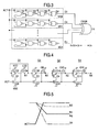
- Fig. 1 shows a circuit diagram of the basic concept of a true random number generating circuit mounted on a semiconductor integrated circuit device according to the present invention.
- CMOS inverter circuits INV1 to INV4 shown in Fig. 1 are configured so as to have identical characteristic within an actually controllable range according to the design and fabrication of the semiconductor integrated circuit device. The technique for making that a plurality of inverters have identical characteristic will be briefly explained below.
- CMOS inverter circuit it is considered that its characteristic is substantially decided by relative conductance between a P-channel type MOSFET and an N-channel type MOSFET constituting the circuit.
- CMOS inverters of the identical characteristic can be configured by MOSFET having an identical ratio W/L wherein W is the channel width W and L is the channel length but different sizes.
- W is the channel width W
- L is the channel length but different sizes.
- a plurality of CMOS inverters INV1 to INV4 are preferably configured in such a way that P-channel type MOSFETs have identical structure and identical size while N-channel type MOSFETs have identical structure and identical size. These elements are fabricated according to the characteristic of the semiconductor integrated circuit device that identical elements are fabricated all at once by the identical fabrication process. Thus, the plurality of CMOS inverters INV1 to INV4 have uniform fabrication irregularities of the semiconductor integrated circuit device such as treatment dimension irregularities, various layer thickness irregularities, and impurities concentration irregularities.
- output voltage of the CMOS inverter circuit INV1 whose input and output are short-circuited reaches a logical threshold value voltage. If all the CMOS inverter circuits have completely identical electric characteristics, the four invert circuits INV1 to INV4 have an identical logical threshold value voltage. However, this is an ideal state. In the actual semiconductor elements, a slight characteristic difference exists and there is a difference between the logical threshold value voltages of the respective inverter circuits INV1 to INV4.
- the significant cause of the irregularities of the logical threshold value of the CMOS inverter circuits can be considered to be the irregularities of MOS transistor characteristics.
- the irregularities of the MOS transistor characteristics care caused by the gate width, the gate insulation film thickness, conductivity decision impurities concentration and its distribution, and the like. These irregularities may be divided into a macro portion and a micro portion.
- the macro portion may be the gate width irregularities between a plurality of wafers in the same lot.
- the present invention mainly consider the micro portion of the irregularities, i.e., irregularities between elements arranged at a comparatively near distance. Such micro irregularities are observed to be generated at random between the elements at a comparatively near distance.
- the irregularities of the logical threshold values of the inverter circuits INV1 and INV2 in Fig. 1 are also random.
- the irregularities of the logical threshold values are not preferable for generating a true random number as will be detailed later.
- characteristic irregularities unique to the respective semiconductor elements can be used as identifiers. That is, when a CMOS inverter circuit is used, the irregularities generated in the logical threshold values can be considered as the irregularities of the N-channel type MOS transistor added by the irregularities of the P-channel type MOS transistor.
- the range of irregularities is made greater and it is possible to effectively generate an identification number or identifier. However, this is not preferable for generating a true random number in response to a noise generated in each node of the semiconductor element.
- the four inverter circuits INV1 to INV4 serve as a basic circuit (or a unit circuit) UC0 and the input and output of the CMOS inverter circuit INV1 are short-circuited to form the logical threshold value voltage VLT1 of the inverter circuit INV1.
- the logical threshold value voltage VLT1 is supplied to the input of the invert circuit INV2.
- its threshold value voltage VLT2 is used as a reference voltage to compare it with the logical threshold value voltage VLT1 and to perform amplification operation.
- the output signal of the inverter circuit INV2 is further amplified by an amplifier circuit formed by the inverter circuits INV3 and INV4 longitudinally connected and is converted into a binary signal.
- the output signal Vout of the second inverter circuit INV2 is further amplified by the third and the fourth inverter circuits INV3, INV4.
- the fourth inverter circuit INV4 it is possible to lastly take out information on the logical level of the amplitude of the power source voltage level.
- the electric signal noise Vnz is quite small and actually, MOS transistors constituting the respective inverter circuits INV1, INV2 have irregular characteristics because of the reasons explained above. Accordingly, the logical threshold value voltages VLT1 and VLT 2 of the first and the second inverter circuits INV1 and INV2 of the basic circuit UC0 are not always identical.
- a differential voltage ⁇ V caused by process irregularities such as ⁇ V exists between the logical threshold value voltages VLT1 and VLT2 of the first inverter circuit INV1 and the second inverter circuit INV2 of the unit circuit UC0.
- the logical threshold value voltage VLT2 of the second inverter circuit INV2 is always greater than the amplitude of the electric signal voltage noise Vnz, the output signal Vout of the second inverter circuit INV2 is always at high level. Accordingly, when the unit circuit UC0 is viewed solely, it is not always guaranteed that the output signal Vout of the second inverter circuit INV2 reflects the electric signal noise Vnz.
- trimming is performed and a compensation circuit is added to correct the aforementioned process irregularities of the two logical threshold value voltages VLT1 and VLT2. This causes problems such as complication of the circuit and increase of the current consumption.
- the inventor of the present invention paid attention on that the irregularities of the transistor characteristics exhibit a random normal distribution. As shown in Fig. 1 , when a plenty of basic circuits are observed, there is a certain probability that there is such a combination that the characteristics of the first inverter circuit INV1 and the second inverter circuit INV2 are quite similar. The inventor found that such a basic circuit sensitively reacts to the electric noise Vnz shown in Fig. 2(a) .
- the logical threshold value voltages VLT1 and VLT2 of the inverter circuits INV1 and INV2 are expressed as a normal distribution.
- their difference VLT1 - VLT 2 forms a normal distribution in which variance of the original logical threshold value voltages VLT1 and VLT2 is doubled.
- the probability that there exists a basic circuit in which the difference VLT1 - VLT 2 of the logical threshold value voltages of the first inverter circuit and the second inverter circuit is smaller than the amplitude of the electric signal noise voltage Vnz is decided by the variance of the logical threshold value voltage VLT of the inverter circuit and the amplitude Vnz of the electric signal noise voltage.
- the average number of basic circuits reflecting the electric signal noise contained in the basic circuit group is the number of basic circuits constituting the basic circuit group multiplied by the aforementioned probability.
- Fig. 1 when output D0 to Dn of a plurality of basic circuits such as UC0 to UCn are inputted to a signal variation detecting circuit EXOR such as an exclusive OR circuit, the output R reacts to a change of any of the output signals D0 to Dn of the connected basic circuits UC0 to UCn and is reversed.
- EXOR such as an exclusive OR circuit
- Each output of the basic circuit group having the plurality of basic circuits UC0 to UCn including at least one basic circuit of a combination of the first inverter circuit and the second inverter circuit whose characteristics are quite similar is inputted to the signal variation detecting circuit EXOR.
- the output R of the signal variation detecting circuit EXOR such as an exclusive OR circuit is revered if one of the outputs D0 to Dn of the basic circuits UC0 to UC1 changes. That is, when the input of the signal variation detecting circuit EXOR is an output of the basic circuit, the output is a true random number reflecting the electric noise of the basic circuit.
- the basic circuit group includes a plurality of basic circuits of a combination of the first inverter circuit and the second inverter circuit whose characteristics are quite similar, there is no correlation between electric signal noises of the respective basic circuit and accordingly, the output R of the signal variation detecting circuit EXOR is similarly a random number. It is possible to obtain a true random number of a higher quality.
- the symbol * is an exclusive OR symbol.
- Fig. 3 shows a basic circuit diagram of a random number generating circuit according to an embodiment of the present invention.
- the inverter circuits INV1 to INV4 in Fig. 1 are replaced by two-input NAND gate circuits G1 to G4.
- the gate circuit G1 an input is connected to an output
- the I/O shared by the gate circuit G1 is connected to one input of the gate circuit G2.
- the output of the gate circuit G2 is connected to one input of the gate circuit G3.
- the output of the gate circuit G3 is connected to one input of the gate circuit G4.
- An operation control signal ACT is commonly supplied to the other inputs of the gate circuits G1 to G4.
- the inverter circuits INV1 to INV4 in Fig. 1 can be considered to be as one type of the logic gate circuits such as the NAND gate circuits G1 to G4. This is because the circuits perform logic operation for reversing the input signal.
- the inverter circuits INV1 to INV4 are used like in Fig. 1 , like the inverter circuits INV1 and INV2, the initial stage side operate in the vicinity of the logical threshold value voltage VLT and DC current flows between the power source voltage VDD and the ground potential.
- the present invention utilizes the normal distribution of the logic threshold value voltages caused by the element process irregularities. Accordingly, it is necessary to operate a comparatively large number of unit circuits and the DC current in the inverter circuits INV1 and INV2 cannot be ignored when lower power consumption should be realized.
- the respective gate circuits G1 to G4 make the output signal high level (logical 1) regardless of the other input signal different from the operation control signal ACT and no DC current is generated in each of the gate circuits G1 and G2. That is, in the circuit of this embodiment, the operation control signal ACT is set to an active level like high level (logical 1) at the timing requiring a random number.
- the respective gate circuits G1 to G4 operate as inverter circuits for forming a reversed signal in response to the other input signal different from the operation control signal ACT.
- the operation control signal ACT by setting the operation control signal ACT to a high level, the operation similar to the basic circuit diagram of Fig. 1 is performed.
- Fig. 4 shows a specific circuit diagram of the true random number generation circuit of Fig. 3 according to an embodiment.
- the gate circuit G1 is formed by N-channel MOSFET Q1 and Q3 connected in series between the output node N1 and the circuit ground potential VSS and P-channel MOSFET Q2 and Q4 connected in parallel between the output node N1 and the power source voltage VDD.
- the gates of the MOSFET Q1 and Q3 are commonly connected to serve as a first input.
- the gates of the MOSFET Q2 and Q4 are commonly connected to serve as a second input.
- the other gate circuits G2 to G4 are similarly configured.
- the gate circuits G1 to G4 are configured so as to have identical characteristic within an actually controllable range in the stage of design and fabrication of the semiconductor integrated circuit device. A brief explanation will be given below on the technique to make a plurality of gate circuits to have identical characteristic.
- the logical threshold values as their characteristic are decided by the P-channel MOSFET and the N-channel MOSFET constituting them.
- CMOS gate circuits having identical characteristic can also be configured by MOSFET having the identical ratio W/L between the channel width W and the channel length L but different sizes.
- the affect of the fabrication irregularities of the semiconductor integrated circuit device to the electric characteristic is different for the element of different size.
- each of the gate circuits G1 to G4 is preferably configured with identical structure and identical size between the elements constituting them, i.e., between the P-channel type MOSFETs and between the N-channel MOSFETs. It goes without saying that the elements are fabricated by the same process all at once according to the characteristic of the semiconductor integrated circuit device.
- the gate circuits G1 to G4 are uniformly affected by the irregularities of the treatment dimension in the fabrication of the semiconductor integrated circuit device, irregularities of thickness of various types of layers, irregularities of impurities concentration, and the like as fabrication irregularities and have the logic threshold value voltage normally distributed.
- a judgment output of the sizes of the logic threshold values of the two gate circuits G1 and G2 is outputted from the gate circuit G2.
- the aforementioned electric signal noise is superposed on the signal transmission and the amplification path, so that an output signal reflected in the electric signal noise is obtained. That is, the voltage (equivalent to the logic threshold value) of the short-circuited I/O node of the gate circuit G1 is supplied as an input bias of the gate circuit G2.
- the output signal reflected in the electric signal noise is amplified by the gate circuits G3 and G4 of the latter stage so as to obtain a binary signal of the CMOS level.
- the gate circuits G3 and G4 merely perform amplification operation and need not be configured in such a way that the P-channel type MOSFETs and N-channel type MOSFETs respectively have an identical structure and an identical size like the gate circuits G1 and G2. However, in this embodiment, they are respectively configured with an identical structure and an identical size mainly from the viewpoint of the circuit design.
- Fig. 5 is a waveform diagram for explaining an example of operation of the true random number generating circuit in Fig. 3 .
- the electric signal noise in the signal transmission path is omitted.
- the gate circuits G1 to G4 substantially enter operation state and the output node N1 of the gate circuit G1 is set to a voltage corresponding to its logic threshold value. It should be noted that the time required for this will be called a convergence time.
- the gate circuit G2 judges the voltage of the node N1 by its logic threshold value and decides a potential of its output node N2.
- the potential of the node N2 is made smaller voltage with respect to the node N1 by the amplification operation of the gate circuit G2.
- the voltage of the node N2 is amplified by the gate circuit G3 and set to a high level like the node N3.
- the voltage of the node N2 is further amplified by the gate circuit G4 to reach the ground potential VSS of the circuit like the node N4.
- the output signal is reversed. That is, like in the Fig. 2(a) , when an electric signal noise reversing the potential difference between the nodes N1 and N2 is generated, i.e., the basic circuit has a combination of gate circuits G1 and G2 having only such a slight voltage difference that the potential difference relationship between the nodes N1 and N2 is reversed by the electric signal noise, the output can generate a true random number reflecting the electric noise of the basic circuit. It goes without saying that the true random number is generated after the convergence time has elapsed. If during the convergence time, it is difficult to obtain a true random number reflecting the inherent minute electric noise while being affected by the transient state of the node of each NAND gate.
- the N-channel MOSFET Q3, A7, Q11, Q15 in Fig. 3 turn OFF, thereby suppressing the through current like when the CMOS inverter circuit is used.
- the advantage of use of the NAND circuit as the gate circuit is that it is a standard element of the CMOS logic LSI which does not limit the product to be applied. That is, since this embodiment is configured by a completely logic description-type circuit, the circuit designing becomes easy.
- the operation control signal ACT is connected to the gates of the N-channel MOSFET Q3, Q7, Q11, Q15 connected in series. However, it is also possible to connect them to the N-channel MOSFET Q1, Q5, Q9, Q13 and to connect the nodes N1, N2, N3 to the gates of the N-channel MOSFET Q3, Q7, Q11, Q15.
- the MOS transistor may fluctuate in an undesired way by such a field stress that its threshold value voltage depends on the electric field intensity and temperature. Especially, the phenomenon called NBTI (Negative Bias Temperature Instability) is remarkably observed in the P-channel type MOSFET. To prevent this, a method to increase the voltage applied to the gate of PMOS during a time other than the target time is often used.
- the gate voltage is set to a fixed voltage so that the logic threshold value judgment operation is performed by the high level of the operation control signal ACT and during a time other than the logic threshold value judgment operation, the operation control signal ACT is set to the low level and the power source voltage is supplied to the gate of the P-channel type MOSFET.
- the gate, the drain, and the source as well as the substrate (channel) all have voltage identical to the power source voltage, which suppresses the fluctuation of the logic threshold value caused by the variation of the MOSFET by time. This is especially advantageous when an identifier is obtained by a combination of the output signals of the unit circuits as has been described above.
- the random number generating circuit has a characteristic that it is basically not affected by the aforementioned fluctuation of the element characteristic or fluctuation of the power source voltage.
- the random number generating circuit of this embodiment among the comparatively plenty of unit circuits, it is sufficient that there exists at least one unit circuit in which the logic threshold value voltages of the gate circuits G1 and G2 are considered to be identical viewed from the electric signal noise. The reason is as follows.
- the logic threshold value voltages of the gate circuits G1 and G2 are no more identical viewed from the electric signal noise, in another unit circuit, the logic threshold value voltages of the gate circuits G1 and G2 are considered to be identical viewed from the electric signal noise.
- Fig. 33 shows a modified example of the true random number generating circuit in Fig. 4 .
- the transistors constituting the NAND have a channel length L and a channel width W greater than the standard size (the minimum dimensions of the normal process).
- the standard size the minimum dimensions of the normal process.
- the sizes of the respective transistors constituting the NAND gate circuits G1 and G2 need not be common.
- the P-channel MOSFET Q2 (Q6) and N-channel MOSFET Q1, Q3, (Q5, Q7) relating to the state during the circuit operation, i.e., affecting the decision of the logic threshold value in the aforementioned active state should have a greater size with a higher priority.
- the corresponding MOSFET of the NAND gate circuits G1 and G2 should have an identical shape.
- the gate circuits G3 and G4 operating as amplifier circuits need not be set as described above.
- the circuit design or the element layout becomes more simple if the same circuits as the gate circuits G1 and G2 are used. This is also advantageous to conceal the existence of the random number generating circuit as will be detailed later.
- Fig. 33(b) shows another implementation method of a circuit which can obtain the same effect as the circuit of Fig. 33(a) . That is, the aforementioned Yuragi phenomenon is suppressed by using a 3-input NAND gate, two P-channel MOSFET and two N-channel MOSFET affecting the decision of the logic threshold value in the active state. This has an advantage that it can be realized by gate parts of standard size without designing a MOS transistor of special size.
- a basic circuit is configured by using a NAND gate but it is also possible to use a NOR gate instead of the NAND gate. In this case, however, the basic circuit is activated when the operation control signal ACT is at the low level (logical 0).
- the degradation caused by electric field stress called NBTI is especially remarkable in the P-channel MOSFET.
- the other elements such as polysilicon FET and organic transistors in which the degradation phenomenon is remarkable not in the P-channel type but in the N-channel type, it is preferable to use the NOR gate.
- the NAND gates G2, G3, G4 in the respective unit circuits UC0 to UCn may be set always at high level (logical 1) by connecting the common control signal ACT connected to them, to the power source VDD. This does not change the basic function of this embodiment.
- Fig. 6 shows a specific circuit diagram of the signal variation detecting circuit EXOR of the true random number generating circuit in Fig. 3 according to an embodiment.
- exclusive OR circuits EX0 to EXn are connected in series to constitute the signal variation detecting circuit EXOR.
- a fixed value such as the low level (logical 0) is given to the other input of the exclusive OR circuit EX0 receiving the output D0 of the unit circuit UC0.
- the output signal of the exclusive OR circuit EX0 is supplied to the other input of the exclusive OR circuit EX1 receiving the output signal D0 of the unit circuit UC1 of the next stage.
- the output signal of the exclusive OR circuit EXn-1 preceding EXn by one is supplied to the other input of the exclusive OR circuit EXn receiving the output signal Dn of the n+1-th unit circuit UCn.
- the signal variation detecting circuit EXOR is configured by a logical gate circuit, it is convenient to use a plurality of exclusive OR circuits as has been described above. However, the configuration is not limited to this. Any configuration may be employed if it can detect a change of the logical level of the output signals D0 to Dn. For example, it is possible to employ a configuration of output signals D0 to Dn and their delay signal forming one-shot pulse.
- Fig. 7 is a circuit diagram of a true random number generating circuit according to another embodiment of the present invention.
- the unit circuits UC0 to UCn are operated in a temporally dispersed way by using a decoder DEC.
- a decoder DEC By using one exclusive OR circuit EX and one flip-flop circuit FF, exclusive logic of outputs of a plurality of unit circuits UC0 to UCn is accumulated, thereby obtaining a true random number RR. It should be noted that by modifying an exclusive OR to a complicated logic, it is possible to obtain a true random number whose generation pattern becomes more difficult to be decoded.
- the decoder DEC is not to be limited to a particular one but is configured by a counter and a decoder. That is, clock CLK is counted by the counter and the counting output is decoded to generate operation control signals DEC0 to DECn for successively activating the unit circuits UC0 to UCn. Alternatively, by using a shift register for successively shifting the initial value corresponding to a selected signal by clock CLK, the operation control signals DEC0 to DECn are formed for successively activating the unit circuits UC0 to UCn.
- a decode output DEC0 is supplied as an operation control signal to the gate circuits G1 and G2.
- the gate circuits G3 and G4 as the amplifier circuits performs amplification operation of the corresponding output signal.
- the output signal of the unit circuit of the preceding stage is passed through and transmitted.
- the output signal of the corresponding gate circuit G2 is transmitted while to the other input, the output signal of the unit circuit of the preceding stage is transmitted.
- the output signal of the corresponding gate circuit G3 is supplied to one input while high level corresponding to the power source voltage is fixedly supplied to the other input.
- the gate circuit G4 substantially operates as an inverter circuit.
- high level corresponding to the power source voltage is fixedly supplied.
- Fig. 8 is a conceptual waveform diagram for explaining an example of operation of the true random number generating circuit in Fig. 7 .
- the operation control signal DEC0 corresponding to the unit circuit UC0 of the initial stage is set to a selection level of high level by the decoder DEC
- the gate circuits G1 and G2 form an output signal, which is amplified by the gate circuits G3 and G4 to form an output signal D0.
- the operation control signals DEC1 to DECn are at non-selection level of low level and the output signals of the gate circuits corresponding to the gate circuit G2 become all high level.
- the gate circuit equivalent tot he gate circuit G3 operates as an inverter circuit only to amplify the output signal from the circuit of the preceding stage.
- the output signal D0 of the unit circuit UC0 of the initial stage is transmitted via the gate circuits of the unit circuits UC1 to UCn to the exclusive OR circuit EX. That is, D1 to Dn are set to the level based on D0.
- the two gate circuits corresponding to the gate circuits G1 and G2 form an output signal, which is amplified by the gate circuits G3 and G4 to form an output signal D1. That is, in the unit circuit of the initial stage, the selection signal DEC0 is at low level, which results in that the output signal of the gate circuit G2 is at high level, and the output signal D0 is fixed to high level. Accordingly, in the unit circuit UC1, as has been described above, amplification is performed by the gate circuits corresponding to the gate circuits G3 and G4.
- the output signal D1 is transmitted to the exclusive OR circuit EX via the gate circuits as the amplifier circuits in the unit circuit of the latter stage like in the aforementioned case. That is, D2 to Dn are set to the level based on D1.
- the selection operation of the third unit circuit UC2 and after up to UCn is also as has been described above.
- the circuit of the embodiment in Fig. 7 actually forms different waveforms from those in Fig. 8 . That is, when the unit circuit UC0 is in the non-selection state, the output signal D0 is at high level. In other words, when the DEC1 has become non-selection level, the output signal D0 forms an output signal of high level corresponding to the non-selection state. This means that when the unit circuits UC1 to UCn are set to the non-selection level, the output signals D1 to Dn also become high level all at once.
- the circuit of the embodiment in Fig. 7 shows a unit circuit group containing (N + 1) unit circuits (basic circuits).
- (n + 1) basic circuits there exists at least one unit circuit of a combination of the first gate circuit G1 (the first inverter circuit INV1) and the second gate circuit G2 (the second inverter circuit INV2) having quite similar characteristics.
- the number of unit circuits having the combination of the first gate circuit G1 and the second gate circuit G2 whose characteristics are quite similar a random number of higher quality is obtained.
- the accumulation of the (n + 1) circuits is multiplied by m, for example, such as (n + 1) x m. That is, pre-outputs D0 to Dn of the unit circuits UC0 to UCn are read out m times so as to decide a 1-bit random number R (RR).
- Fig. 9 shows a true random number generating circuit according to the present invention and a circuit diagram of its component circuit according to an embodiment.
- M x N unit circuits (component circuits) as shown in Fig. 9(b) are arranged in a matrix.
- One row is connected like the circuit in Fig. 7 and its output unit has a NAND gate circuit G0 selected by the row selection signal and clocked inverter circuit CN0.
- M unit circuits constituting each of the rows corresponding ones are commonly selected by column selection signals Co to CM-1 formed by a column decoder.
- N unit circuits arranged in the row direction one is selected by the row selection signals R0 to RN-1 formed by a row decoder.
- the row selection signals R0 to RN-1 are also used as selection signals of the row selection circuit formed by the NAND gate circuit G0 and the clocked inverter circuit CN0.
- the clocked inverter circuit CN0 constituting the selection circuit becomes output high-impedance state when it is the non-operation state. Accordingly, the output signals of the N clocked inverter circuits are commonly connected and the output signal of the clocked inverter circuit corresponding to the selected one row is transmitted to the NAND gate circuit G11.
- Clock CLK is supplied M-mal counter via the NAND gate circuit G10 and the inverter circuit 10 in which the gate is controlled by the operation control signal ACT.
- the M-mal counter performs counting operation 0 to M-1 corresponding to the clock CLK.
- the row decoder forms the selection signals C0 to CM-1 and the output signals of the unit circuits are output in serial like in the embodiment of Fig. 7 .
- N-mal counter Since the carry signal of the M-mal counter is supplied to the N-mal counter, N-mal counter performs counting operation in accordance with one turn of the M-mal counter. Thus, when the M unit circuits arranged in the row direction are read out, the row selection is switched. From 0 th to (RN - 1)-th row, N unit circuits are read respectively.
- all the unit circuits are read out by the M x N cycles and accordingly, it is possible to generate a 1-bit true random number from the output RR by the M x N cycles. This is repeated by K times so as to obtain a K-bit true random number.
- the number of M x N is selected in such a manner that among the M x N unit circuits, there exists at least one unit circuit responding to the electric signal noise. It should be noted that during the K-time repetitions, it is possible to extract J (0 ⁇ J ⁇ K) random numbers. In this case, however, the random number bit extraction cycle should be apart at least M x N cycles.
- the number M is selected in such a manner that among the M unit circuits, at least one unit circuit generating the true random number exists, it is possible to obtain a 1-bit true random number RR for each M cycle (for each row). Accordingly, it is possible to configure a true random number generating circuit generating an N-bit true random number by M x N cycles.
- Fig. 9(b) shows a specific circuit diagram of a circuit element in Fig. 9(a) according to an embodiment.
- the unit circuit is formed by the gate circuits G1 to G4 shown in Fig. 7 and gate circuits G5 and G6 for providing the row/column selection function.
- a column selection signal Ci and a row selection signal Ri are supplied to the two inputs of the NAND circuit G5.
- an output signal Di of the unit circuit of the preceding by-one stage in the row is supplied.
- Fig. 9(c) shows a specific circuit diagram of the circuit element in Fig. 9(b) according to another embodiment.
- the unit circuit is formed by a 3-input NAND gate replacing the gate circuits G1 to G4 shown in Fig. 9(b) and Fig. 7 and the NAND gate also has the row/column selection function.
- the column selection signal Ci and the row selection signal Ri are supplied to two of the three inputs of the NAND gate circuits G5 and G6.
- the output signal Di of the unit circuit of the preceding by-one stage in the row is supplied.
- the clocked inverter circuit CN in Fig. 9(a) is formed by the P-channel MOSFET Q1, Q2 and N-channel MOSFET Q4, Q3 connected in series between the power source voltage VDD and the circuit ground potential VSS.
- the gates of the P-channel MOSFET Q1 and the N-channel MOSFET Q3 are commonly connected to serve as an input terminal A.
- the drains of the P-channel MOSFET Q2 and the N-channel MOSFET Q4 are commonly connected to serve as an output terminal B.
- a control signal supplied from the terminal C is supplied to the gate of the N-channel MOSFET Q4, so that the aforementioned control signal is reversed by the inverter circuit INV12 and supplied to the gate of the P-channel MOSFET Q2.
- the N-channel MOSFET Q4 and the P-channel MOSFET Q2 When the selection signal such as a row selection signal supplied from the terminal C is high level, the N-channel MOSFET Q4 and the P-channel MOSFET Q2 enter the ON state and the output terminal B outputs an output signal corresponding ON/OFF of the N-channel MOSFET Q3 and the P-channel MOSFET Q1 receiving the input signal from the input terminal A.
- the selection signal such as a row selection signal supplied from the terminal C is high level
- the N-channel MOSFET Q4 and the P-channel MOSFET Q2 simultaneously enter the ON state and the input signal from the input terminal A complementarily sets the N-channel MOSFET Q3 or the P-channel MOSFET Q1 to the ON state.
- a low level or a high level is outputted from the output terminal B.
- the clocked inverter circuit CN in Fig. 9(a) may be a transfer gate circuit shown in Fig. 9(e) .
- the clocked inverter circuit CN is formed by the P-channel MOSFET Q5 and the N-channel MOSFET Q6 connected in series between the input terminal A and the output terminal B.
- the control signal supplied from the terminal C is supplied to the gate of the N-channel MOSFET Q6 and the control signal is reversed by the inverter circuit INV14 before being supplied to the gate of the P-channel MOSFET Q5.
- the P-channel MOSFET Q5 and the N-channel MOSFET Q6 enter the ON state and the input signal from the input terminal A is outputted from the output terminal B.
- the selection signal such as the row selection signal supplied from the terminal C is high level
- the N-channel MOSFET Q4 and the P-channel MOSFET Q2 simultaneously enter the ON state and the input signal from the input terminal A complementarily sets the N-channel MOSFET Q3 or the P-channel MOSFET Q1 to the ON state.
- a low level or a high level is outputted from the output terminal B.
- the selection signal such as the row selection signal supplied from the terminal C is low level
- the N-channel MOSFET Q4 and the P-channel MOSFET simultaneously enters the OFF state and the output terminal B becomes high impedance.
- Fig. 10 shows a circuit diagram of a true random number generating circuit and its element circuit according to another embodiment of the present invention.
- a plurality of the unit circuits shown in Fig. 10(b) are arranged in a matrix of M (columns) x N (rows).
- One row is connected like the circuit in Fig. 7 and its output unit has the NAND gate circuit G0 and the exclusive OR circuit EX0.
- the NAND gate G0 has the other input which is connected to the power source VDD and always in the high level (logical 1).
- the corresponding unit circuits are commonly selected by the column selection signals C0 to CM-1.
- Clock CLK is supplied to the M-mal counter via the NAND gate circuit G10 and the inverter circuit INV10 whose gates are controlled by the operation control signal ACT.
- the M-mal counter performs counting operation 0 to M-1 corresponding to the clock CLK.
- the column decoder forms the selection signals C0 to CM-1 and the output signals of the unit circuits of the respective rows sharing the Ci formed by N rows are outputted serially like in the embodiment of Fig. 7 .
- the output of the NAND gate circuit G0 is connected to the exclusive OR circuit EX0 and the other input of the EX0 is connected to. Furthermore, the output of the exclusive OR circuit EX0 is connected to the exclusive OR circuit of the adjacent row. The outputs of all the exclusive OR circuits are successively connected to the adjacent row in the longitudinal way. A fixed value such as the high level (logical 1) is given to the other input of the exclusive OR circuit. Thus, if any one of the N output signals generated by the N-row unit circuits sharing the selected Ci changes, the output signal RA of the exclusive OR circuits connected vertically.
- the output signal RA becomes a value reflecting the electric noise of the N unit circuits (basic circuits) by one-cycle operation.
- the unit circuits since all the unit circuits are read by M cycles, it is possible to generate a 1-bit true random number from the output RR by M cycles. By repeating this K times, it is possible to obtain a K-bit true random number.
- the number M x N is selected so that at least one unit circuit responding to the electric signal noise exists among the M x N unit circuits. It should be noted that during the K times of repetition, it is possible to extract J (0 ⁇ J ⁇ K) random numbers. In this case, however, each random number bit extraction cycle should be apart at least by M cycles.
- Fig. 10 (b) shows a specific circuit diagram of the circuit element in the true random number generating circuit shown in Fig. 10(a) according to an embodiment.
- the column selection signal Ci is supplied to one of the two inputs of the NAD gate circuits G1 and G2.
- the output signal Di of the unit circuit of the preceding by-one stage in the row is supplied to the gate circuit G3 like in the unit circuit of Fig. 7 . This set only one unit circuit whose column is in the selected state enters the aforementioned operation state.
- Fig. 11 is a brief waveform diagram for explaining an example of the operation of the true random number generating circuit of Fig. 9 .
- the clock CLK is inputted when the operation control signal ACT is at the activated level of high level, the column selection signals C0 to CM-1 are outputted from the column decoder in response to that.
- the N-mal counter has a count value zero and the row selection signal R0 of the 0-th row is set to the selection level. Accordingly, the output signals of the units circuits of the 0-th row are outputted serially corresponding to the column selection signals C0 to CM-1.
- the carry signal increments the N-mal counter by +1.
- the 0-th row R0 is set to the non-selection state and the first row R1 is set to the selection state instead.
- the true random number RR is decided by the exclusive OR of the serial output R of the unit circuit and the output preceding by one. It should be noted that the operation waveform diagram of the true random number generating circuit of Fig. 10 is similar to that of Fig. 9 and is omitted. The difference from Fig. 9 is that the selections signals R0 to RN-1 are absent. Thus, there is no need of operation for advancing the N-mal counter and M cycles are required for selecting all of the M x N unit circuits (basic circuits).
- Fig. 12 shows a conceptual diagram of a true random number generating circuit according to another embodiment of the present invention.
- a random number is generated by a method using a combination of the arithmetic random number generating circuit and the physical phenomenon according to the present invention.
- the arithmetic random number generating circuit can be realized by a circuit of comparatively small size but the quality of the random number obtained by that is not high. Especially it has an essential defect that a periodicity appears when a plenty of random numbers are obtained.
- the periodicity may be reduced by inserting the irregular element in response to the electric signal noise in the random number generating circuit according to the present invention.
- Fig. 13 shows a circuit diagram of the initial value generating circuit of Fig. 12 according to an embodiment.
- This embodiment is basically identical to the embodiment of Fig. 6 .
- the difference from Fig. 6 is that the exclusive OR circuits EX0 to EXn are replaced by flip-flop circuits FF0 to FFn.
- the initial values such as D0 to Dn are obtained from the flip-flop circuits FF0 to FFn.
- Fig. 14 shows a circuit diagram of the initial value generating circuit of Fig. 12 according to another embodiment.
- This embodiment is basically identical to the embodiment of Fig. 6 .
- the difference from Fig. 6 is that a 1-bit random number is outputted from the flip-flop circuit FF by the activation signal ACT. That is, in this embodiment, a 1-bit random number is used as the initial value of the arithmetic random number generating circuit.
- Fig. 15 shows a waveform diagram for explaining the operation of the initial value generating circuits of Fig. 13 and Fig. 14 .
- the operation control signal ACDT becomes high level
- the respective unit circuits UC0 to UCn output the output signals R0 to Rn.
- the operation control signal ACT becomes from high level to low level
- the random numbers D0 to Dn corresponding to the aforementioned output signals R0 to Rn are supplied to the flip-flop circuits FF0 to FFn and a random number of a plurality of bits D0 to Dn containing fixed values is outputted.
- the output signals R0 to Rn of the unit circuits UC0 to UCn are supplied to the exclusive OR circuit EX0 to EXn and a 1-bit random number corresponding to the signals R0 to Rn is outputted via the exclusive OR circuits EX0 to EXn. Accordingly, when the operation control signal ACT has become from high level to low level, a random number generated then is supplied to the flip-flop circuit FF and a 1-bit random number DM is outputted.
- Fig. 16 shows a circuit diagram of a true random number generating circuit according to another embodiment of the present invention.
- This embodiment is formed by the true random number generating circuit shown in Fig. 9 and an output terminal for outputting an identifier F. That is, the M x N output signals outputted from the M x N unit circuits are outputted as an identifier F.
- the identifier F is held in an appropriate storage circuit and registered in a management system.
- the collation method of this identifier F should allow fluctuation of the identifier corresponding to the true random number responding to the electric signal noise in addition to the difference in the environment and condition between the registration time and the collation time.
- An appropriate storage circuit stores the identifier F at the moment when the power of the semiconductor integrated circuit device having the true random number generating circuit is turned ON or immediately after the operation activation signal ACT is activated, so that the identifier is used as a number to be identified.
- Registered identification numbers are successively acquired from the management system. A registered identification number is compared to the number to be identified.
- a pair of registered identification number and the number to be identified having a small difference as the comparison result is made a matched candidate. This operation is repeated for the registered identification numbers registered in the management system and finally, the one of the registered identification number having the least difference becomes the most powerful candidate.
- the output pattern of "0" and "1" of the corresponding bit is unique to each of the registered identification numbers. It is possible to decide whether identification numbers have been outputted from the same semiconductor integrated circuit device by checking the ratio of the coincidence of the number of bits constituting the pattern. Since the fluctuation of the identification number caused by the difference of the environments between the registration time and the collation time and the random number bit is allowed, it is possible to identify a chip by making the one having the least total of the differences between the numbers to be identified and the registered identification numbers as a candidate of coincidence.
- Fig. 17 shows a circuit diagram of a true random number generating circuit according to an embodiment of the present invention.
- This embodiment has a basic configuration identical to the embodiment of Fig. 9 .
- a test circuit is attached to the true random number generating circuit for testing itself.
- the inspection method of this test circuit decides the number of unit circuits having the first gate circuit G1 (the first inverter circuit INV1) and the second gate circuit G2 (the second inverter circuit INV2) having quite similar characteristics contained in the unit circuit group and guarantees to surely catch the electric signal noise based on the physical phenomenon.
- the circuit node capable of acquiring the output signal from each unit circuit i.e., the signal R of the output terminal (one of the inputs of the exclusive OR circuit EX) of the inverter circuit INV1 is supplied to a reversion inspector and the detected signal H is counted by a counter.
- the counting output C is compared by a comparator to obtain a judgment result M.
- a column selection signal is formed by a (4+M)-mal counter.
- the (4+M)-mal counter repeatedly selects the same unit circuit four times and then proceeds to selection operation of the next unit circuit.
- Fig. 18 is a timing diagram for explaining an example of the operation of the aforementioned test circuit.
- a test signal TS is set to high level to instruct the (4+M)-mal counter operation.
- the reversion detector and the counter are set to the initial state or to the initial value.
- the operation control signal ACT is set to high level so that the random number generating circuit enters the operation state.
- Clock CLK is supplied and read is started at the first unit circuit and then read is continued successively.
- the (4+M)-mal counter selects the same unit circuit four times continuously for the clock CLK 1 to 4.
- the same signal R is outputted four times.
- the reversion detector When the fixed value is outputted, the reversion detector does not perform reversion detection and the counter is not incremented. On the contrary, when there exists one forming the output signal R in response to the electric signal noise Vnz like in Fig. 2(a) , the number of reversions during the four accesses is 3 times at maximum. When at least one reversion is performed, the detection result is true. In the figure, the output signal R changes at the second cycle and the fourth cycle. Thus, on the reversion detector, the level of the output H is changed each time.
- the output H changes at least once
- the result is true and the counter value C0 is changed from low level to high level and is incremented by 1.
- Next unit circuit is selected in the unit circuit group and the aforementioned detection operation is repeatedly performed up to the last unit circuit.
- the number (?) of the counters is greater than a predetermined value
- the value of the detection result M is made true (high level).
- the predetermined value is basically 1 but it is preferably 2 or 3 or above for safely.
- the comparator detects that the counter outputs C0 and C1 both become high level at the (K-1)-th cycle of the clock CLK and the aforementioned inspection result M is decided to be high level. Then, like in Fig. 2(a) , it is confirmed that there exist at least four which form the output signal R in response to the electric signal noise Vnz.
- one unit circuit is accessed four times by CLK pulse for inspection.
- the number accesses may be twice.
- a (2+M)-mal counter is used.
- it operates as an M-mal counter according to the low level of the test signal TS.
- the counter may be operated directly as the (4+M)-mal counter or the (2+M)-mal counter. In this case, the read cycle is increased by 4 times or twice.
- FIPS140-2 As specification of security products by a governmental organization, there is FIPS140-2 suggested by NIST (National Institute of Standards and Technology). This defines security requirements (FIPS PUB 140-2, Security Requirements for Cryptographic Modules) to be satisfied by the cryptographic modules of the articles purchased by the government.
- FIPS PUB 140-2 Security Requirements for Cryptographic Modules
- the random number there is a quality inspection standard by the statistical method. When using the method, the dedicated circuit size for implementing the method is comparatively large and comparatively long time is required for inspection by a semiconductor test device.
- the test circuit having the random number generating circuit according to the present invention can make a judgment at the moment when a circuit is completed on a semiconductor wafer without connecting it to a tester having the aforementioned test function.
- the semiconductor integrated circuit device can make a judgment by itself upon shipment.
- it can be checked when necessary or periodically to decide whether the true random number generating circuit can operate normally. This provides a true random number generation with a high reliability. All these can be performed because they are supported statistically.
- a diagnosis (test) of a true random number generating circuit is equal to evaluation of the quality of the random number and requires a certain statistic process.
- there are significant problems such as a test device, a test time, and a long-term reliability guarantee.
- the true random number generating device is mounted on a LSI or a final system, it is quite important whether the circuit itself is normally operating. This is because, unless a true random number of a high quality can be obtained, security is in danger.
- testing or monitoring the true random number generating circuit is a large load for a system in operation. For such a technical problem, the true random number generating circuit of the present invention can solve these problems with the aforementioned simple configuration.
- Fig. 19 shows a circuit diagram of a true random number generating circuit according to an embodiment of the present invention.
- This embodiment has a basic configuration identical to the embodiment of Fig. 9 .
- an oscillation pulse formed by an oscillator is used as the clock.
- Fig. 20 shows an operation waveform diagram of the true random number generating circuit of Fig. 19 .
- the activation signal ACT causes the oscillator to generate a pulse of a particular cycle Tosc.
- the unit circuits in the unit circuit group are successively selected and a random number is generated in the RR signal.
- the start signal ST is shifted to the high level, the random number of the RR signal is extracted from the output RY.
- the relationship between the cycle Tc of the start signal and the cycle Tosc of the oscillator is [Tc] ⁇ [Tosc] x [n] since output signals should be read from all the unit circuits.
- [n] represents the number of units circuits (M x N) in the unit circuit group.
- the oscillator output pulse OSC maybe a system clock of the LSI on which the true random number generating circuit is mounted.
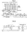
- Fig. 21 shows a circuit diagram of a true random number generating circuit according to an embodiment of the present invention.
- This embodiment has basic configuration identical to the embodiment of Fig. 19 .
- the start signal ST is omitted and the operation state is set in by the operation control signal ACT.
- a shift register is arranged immediately before the output so as to generate a random number RAi formed by parallel bits.
- Fig. 22 shows an output unit of a random number generating circuit according to another embodiment of the present invention.
- the shift register in Fig. 21 is replaced by a memory.
- the memory used in the figure is a so-called serial input/parallel output type memory.
- the true random number generating circuit When the control signal ACT is at the high level, the true random number generating circuit generates a 1-bit true random number from RR for each clock M x N cycle. Simultaneously with this, the memory is a serial input mode and acquires a true random number from the input SI and accumulates it.
- SE is a control input for switching the mode of the memory,. When high level, the mode is serial input mode. When low level, the mode is parallel input mode. SI is a serial data input. CK is a synchronization signal input for acquiring a serial input. AD is an address input for selecting the memory space when the mode is parallel output mode. DT is a parallel data output.
- the memories shown in Fig. 22 may be FIFO (First In First Out) type memories or asynchronous memories capable of simultaneously performing the serial input and the parallel input.
- FIFO First In First Out
- asynchronous memories capable of simultaneously performing the serial input and the parallel input.
- Fig. 23 shows an operation waveform diagram of the true random number generating circuit shown in Fig. 21 .
- the operation control signal ACT causes the circuit to enter the operation state.
- the shift register performs 1-bit shift operation and acquires the generated true random number RR.
- the unit circuit group consisting of 0 to 7 is read out and 8-bit random numbers D0 to D7 can be outputted in parallel.
- Fig. 24 shows a chip configuration of the true random number generating circuit according to an embodiment of the present invention.
- the true random number generating circuit is configured by a single IC.
- the IC has power terminals VCC, VSS a clock input terminal CLK, an operation control signal terminal RST, and a true random number output terminal RR as external terminals.
- the clock terminal CLK is omitted.
- the IC having a test circuit includes a judgment output terminal, a test mode input terminal, and the like.
- the judgment output terminal can be shared (?) by the random number output terminal RR.
- the IC chip may be sealed in one packet or mounted on the same substrate of another IC and sealed (multi-chip IC), or can be directly mounted on the system.
- Fig. 25 is a block diagram of a semiconductor integrated circuit device according to an embodiment of the present invention.
- the respective circuit blocks in this embodiment are drawn in accordance with the geometrical circuit arrangement on the actual semiconductor substrate.
- a combination of a plurality of circuit blocks has a particular signal processing function.
- the true random number generating circuit is mounted on the semiconductor integrated circuit device having such circuit blocks.
- the clock required for the true random number generating circuit may be the clock formed by the clock generating circuit arranged on the semiconductor integrated circuit device or the clock supplied from an external terminal.
- the clock supply is not required.
- Fig. 26 is a block diagram of a semiconductor integrated circuit device according to another embodiment of the present invention.
- the respective circuit blocks are drawn in accordance with the geometrical circuit arrangement on the actual semiconductor substrate.
- This embodiment is intended for a one-chip microcomputer having an MPU (micro-processing unit) at the center.
- This microcomputer has BUS (address bus, data bus, and control bus) connected to the MPU, a RAM (random access memory), a ROM (read only memory), a DMAC (direct memory access controller), a TIM (timer), an ADC (analog/digital converter), a DAC (digital/analog converter), and the aforementioned true random number generating circuit.
- the true random number generating circuit of the present invention can be realized all by the standard CMOS logic circuits. This reduces the load required for a complicated analog circuit design or LSI mounting, reduces the product cost, and improves the reliability. Moreover, it is possible to provide a module strong against cracking which is the biggest problem in the security. This is because only the standard logic circuits are used and it is possible to obtain a stealth effect to avert an attack target in the LSI. That is, there is no circuit pattern characteristic like when an analog circuit is used. Besides, when a random number is extracted via the bus in like in the aforementioned case, the stealth effect is further enhanced.
- Fig. 27 shows a configuration of the true random number generating circuit according to an embodiment of the present invention.
- Fig. 28(a) shows a circuit block configuration and Fig. 27(b) shows a layout configuration.
- n pieces of true random number generating circuits shown in Fig. 7 are arranged. That is, n true random number generating circuits 0 to n-1 are arranged and the respective output signals R0, R1 to Rn-1 pass through a multiplexer MUX so that one signal is selected to output a true random number RM.
- a multiplexer is sandwiched two true random number generating circuits, which enables effective circuit arrangement.
- one circuit block in the true random number generating circuit represents, for example, one of the aforementioned unit circuits.
- the multiplexer sandwiched by two true random number generating circuits may have a comparatively simple configuration for selecting one of two. Accordingly, at the portion where the multiplexer is arranged, a selection signal generating circuit such as the decoder is arranged.
- a random number R when a random number R is obtained by n unit circuits in the true random number generating circuit of this embodiment, a 1-bit random number R requires output signals from all the unit circuits and spends n cycles.
- n random number generating circuits are provided like in this embodiment in accordance with the n cycles required for obtaining the one random number, it is possible to generate a random number with a high frequency synchronized with the clock CLK. However, this requires n dummy cycles counted from the start of operation by the operation control signal.
- Fig. 28 is a timing diagram showing an example of operation of the true random number generating circuit shown in Fig. 27 .
- the true random number generating circuit of Fig. 27 in order to read out the first random number generating circuit, random numbers R0 to Rn-1 are outputted from the respective true random number generating circuit after n cycles (n clocks). Accordingly, by selecting one after another in synchronization with the clock CLK by the multiplexer MPX, it is possible to obtain a true random number RM (R0, R1, R2 ... Rn-1, R0', R1', R2'....) of high bit rate synchronized with the clock CLK.
- Fig. 29 shows an external view of an IC card according to an embodiment of the present invention.
- the IC card includes a card 101 formed by a plastic case and an IC card chip formed by a 1-chip microcomputer or the like (not depicted) mounted in the card 101.
- the IC card also has a plurality of contacts (electrodes) 102 connected to an external terminal of the IC card chip.
- the plurality of contacts 102 are a power terminal VCC, a power reference potential terminal VSS, a reset input terminal RES bar, a clock terminal CLK, a data terminal I/O - 1/IRQ bar, an I/O - 2/IRQ bar which will be detailed with reference to Fig. 30 .
- the IC card receives power from an externally connected device such as a reader/writer (not depicted) via the contacts 102 and performs data communication with the externally connected device.
- Fig. 30 is brief block diagram of the IC card chip (microcomputer) mounted on the IC card according to an embodiment of the present invention.
- the circuit blocks in Fig. 30 are formed on a single semiconductor substrate such as monocrystal silicon.
- the IC card chip according to the present invention has basically identical configuration as a microcomputer.
- the chip is basically formed by a clock generating circuit, a central processing unit (hereinafter, simply referred to as CPU), a ROM (Read Only Memory), a RAM (Random Access Memory), a nonvolatile memory (EEPROM), and other memories, a coprocessor (encryption/decryption device) for performing encryption and decryption, and an I/O port.
- CPU central processing unit
- ROM Read Only Memory
- RAM Random Access Memory
- EEPROM nonvolatile memory
- coprocessor encryption/decryption device
- the clock generating circuit receives an external clock CLK supplied via the contacts 102 in Fig. 29 from a reader/writer (externally connected device) (not depicted), forms a system clock signal synchronized with the external clock signal, and supplies it inside the chip.
- the CPU performs logic operation and arithmetic calculation and controls the system control logic, the random number generator, the security logic, and the timer.
- the memories such as the RAM, the ROM, and the EEPROM store programs and data.
- the coprocessor is formed by a circuit compatible with the DES encryption method and the like.
- the I/O port performs communication with the reader/writer.
- the data bus and the address bus connect the respective components.
- the ROM is a memory in which the stored content is fixed in the nonvolatile way and which is mainly used for storing programs.
- a volatile memory (hereinafter, referred to as a RAM) is a memory in which stored information can be freely rewritten and the stored content disappears when power supply is interrupted. When the IC card is pulled out of the reader/writer, the power supply is interrupted and the contents of the RAM cannot be held.
- the nonvolatile memory (hereinafter, referred to EEPROM (Electrical Erasable Programmable Read Only Memory)) is a memory in which the content can be rewritten. The information written there is held even when power supply is interrupted.
- the EEPROM is used for storing data which need be rewritten and held when the IC card is pulled out of the reader/writer. For example, when the IC card is used as a prepaid card, the number of prepaid times is rewritten each time the card is used. In this case, the number of prepaid times should be held even after the IC card is pulled out of the reader/writer and is held in the EEPROM.
- the CPU has configuration identical to that of a so-called microprocessor. That is, although the details are not depicted, the CPU includes a command register, a micro command ROM for decoding a command written in the command register and forming various micro commands or control signals, operation circuits, general-purpose registers (RG6 and the like), a bus driver connected to the internal BUS, and an I/O circuit such as a bus receiver.
- the CPU reads out a command stored in the ROM or the like and performs operation corresponding to the command.
- the CPU performs control for acquisition of external data inputted via the I/O port, read out of a command from the ROM and data such as fixed data required for executing the command, write and read of data to/from the RAM an the EEPROM.
- the CPU receives a system clock signal generated from the clock generating circuit and operates at the operation timing and cycle decided by the system clock signal.
- the CPU has the main internal portion including CMOS circuits formed by P-channel MOSFET and N-channel MOSFET.
- the CPU includes a CMOS static circuit capable of performing static operation such as a CMOS static flip-flop and a CMOS dynamic circuit capable of performing precharge to the signal output node and signal output to the signal output node in synchronization with the system clock signal.
- the coprocessor adds a sign bit to the plain text data handled inside so as to have both of positive/negative states.
- the data is modified at random for each sign.
- Calculation not affected by the sign (such as exclusive OR) is performed as it is while ignoring the sign.
- calculation affected by the sign (such as calculation using a conversion table)
- a calculation circuit for the positive state and a calculation circuit for the negative state are prepared and the output of the calculation circuits is selected according to the data sign.
- the DES Data Encryption Standard
- the DES algorithm can be roughly divided into a plain text data flow and a key data flow.
- a transportation (signal replacement) called IP is performed and then the data is divided into upper 32 bits and lower 32 bits.
- the transportation/character conversion process is repeated 16 times.
- the upper 32 bits and the lower 32 bits are unified and transportation called IP -1 is performed to obtain an encrypted text.
- encryption and decryption can be realized by the same process.
- the key scheduling is different between encryption and decryption. Details of the key scheduling are omitted.
- the key data 48-bit key scheduling data is outputted for each stage.
- the same internal operation is always performed for the same plain text.
- the internal signal varies depending on the input signal and it is possible to easily perform the statistical process by the DPA (Differential Power Analysis). That is, in the DPA method, the encryption key is estimated by statistically processing the consumed current waveform. For example, an encryption key assumed is applied to a certain part of the DES and the consumed current waveform is measured and statistically processed while changing the plain text. This work is repeated while changing the encryption key. When a correct key is applied, the current waveform shows a large peak.
- JP-A-2000-066585 As a countermeasure for DES decryption by the aforementioned DPA, there is JP-A-2000-066585 .
- a pair of a pattern of a mask "a” and a mask pattern of the inversion bit is provided so that one of them is selected at random by a switch each time encryption is performed, thereby masking the bit depending on the plain text in the device so as to remove the affect of the mask "a" from the encrypted text before being outputted.
- the aforementioned mask should not be a particular pattern in order to prevent decryption by the DPA.
- a random number generated by a random number generator is used so that a pattern of a plural bits is not a particular pattern.
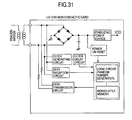
- Fig. 31 shows a block diagram of a non-contact IC card according to an embodiment of the present invention.
- Fig. 31 also shows a coil (antenna) of a reader/writer provided as an external device for the non-contact IC card.
- the LSI mounted on the non-contact IC card includes the blocks depicted and function blocks such as a memory and a microcomputer, which are expressed as a logic circuit and a nonvolatile memory.
- the circuit elements constituting the respective blocks of the LSI may be, for example, formed on a single semiconductor substrate like a monocrystal silicon by the MOSFET (metal oxide semiconductor field effect transistor) integrated circuit fabrication technique.
- MOSFET metal oxide semiconductor field effect transistor
- the term MOSFET is used as a general name for insulation gate type field effect transistors.
- the LSI is laminated by a predetermined protection film and then mounted on a card surface as a substrate of the non-contact IC card, which is further covered by a film.
- the non-contact IC card of the present embodiment may be, for example, a so-called adhesion type non-contact IC card including a coil-shaped electricity-receiving coil (card side antenna) formed on a card surface by using a copper foil, for example, and an LSI connected to the electricity-receiving coil via a predetermined wiring layer.
- the LSI is formed by a rectifier circuit including four diodes bridged, a smoothing capacitor for smoothing the rectified voltage of the rectifier circuit, and a stabilizing power supply circuit, which form an operation voltage VDD of the internal circuit including the aforementioned logic circuit and the nonvolatile memory.
- a clock generating circuit, a data receiving circuit, and a data transmitting circuit are provided substantially in a parallel form.
- the rectifier circuit formed by the diode bridge circuit rectifies an AC signal, i.e., a carrier transmitted as power to the electricity receiving coil of the non-contact IC card by the electromagnetic coupling with a transmission coil (antenna) of the reader/writer, generates DC power voltage VDD from voltage smoothed by the smoothing capacitor by the stabilizing power supply, and supplies it as power to the respective function blocks of the LSI.
- a power-ON reset circuit detects a rise of the power voltage VDD, i.e., detects the connection with the reader/writer and resets the logic circuit register and latch circuit so as to normally perform data reception and transmission.
- the data receiving circuit receives and demodulates data transmitted, for example, by frequency-modulating the carrier and transmits it as internal input data to the internal circuit of the LSI.
- the output data formed in the internal circuit frequency-modulates the carrier by the data transmission circuit and transmits it to the reader/writer.
- the aforementioned internal circuit (logic circuit), the data receiving circuit, and the data transmitting circuit requires a clock signal for the operation sequence control and signal reception and transmission in addition to the aforementioned operation voltage VDD.
- the clock generating circuit generates a clock signal by using the AC signal as a pulse signal.
- the logic circuit unit includes a random number generator, which is used for data transmission and reception to/from outside.
- the DC power voltage VDD has a small current supply capacity and the power consumption by the random number generator also should be small.
- the aforementioned random number generating circuit successively operates the unit circuits and power consumption can be made small. Accordingly, the random number generator of this embodiment is appropriately mounted on the aforementioned non-contact IC.
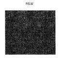
- Fig. 32 shows random number two-dimensional dispersion diagram of a random number generated by the random number generating circuit according to the present invention.
- 0 and 1 of 200 x 200-bit random number are expressed corresponding white dots and black dots.
- 128 unit circuits (basic circuits) are used to constitute a circuit by a normal CMOS process.
- Fig. 32 shows a random number two-dimensional dispersion diagram read by a scanner with 400 dpi and is slightly different from the actual random number two-dimensional dispersion diagram. However, Fig. 32 roughly shows the random number two-dimensional dispersion, which shows that no particular pattern exists. That is, the random number has a high quality. Moreover, the result of the random number inspection by the aforementioned FIPS140-2 is as follows. The length of the random number used at one inspection is 20,000 bits and this is repeated 600 times. The inspection results were all satisfactory.
- IPsec Internet Protocol security
- IPv6 When the IPv6 is spread, an IP number can be assigned to a personal computer and a mobile telephone as well as an automobile of home electric appliance. In this case, it is necessary to easily generate a random number of high quality, i.e., a true random number in the devices.
- the true random number generating circuit according to the present inventions is entirely realized only by the standard CMOS logic circuits. This reduces the load required for a complicated analog circuit design and LSI mounting and contributes to reduction of the cost and improvement of reliability.
- Fig. 34 shows a circuit diagram of an application concept of the basic concept of the true random number generating circuit shown in Fig. 1 and mounted on the semiconductor integrated circuit device according to the present invention.
- a true random number is based on the electric signal noise generated in the INV1 and INV2 in each of the basic circuits.
- the first inverter INV1 is shared and the second inverter is spread to the respective basic circuits.
- Fig. 35 shows a circuit diagram of another application concept of the applied basic concept of the true random number generating circuit shown in Fig. 34 and mounted on the semiconductor integrated circuit device according to the present invention.
- the inverter circuits INV1 to INV14 of Fig. 34 are replaced by 2-input NAND gate circuits G1 to G14.
- the gate circuit G1 has one input and the output coupled with each other.
- the shared input/output of the gate circuit G1 is connected to one input of the gate circuit G02 in the basic circuit.
- the output of the gate circuit G02 is connected to one of the inputs of the gate circuit G03.
- the output of the gate circuit G03 is connected to one of the inputs of the gate circuit G04.
- the other inputs of these gate circuits G02 to G04 are connected to a power source VDD and always at high level (logical 1).
- the inverter circuits INV1 to INV14 in Fig. 34 can be considered as a type of the logic gate circuit such as the NAND gate circuits G1 to G14. This is because the logical operation for inverting the input signal is performed.
- the inverter circuits INV1 to INV14 are used like in Fig. 34 , the inverter circuits INV1 and INV02 operate in the vicinity of the logical threshold value voltage VLT at the initial stage side and DC current flows between the power voltage VDD and the circuit ground potential.
- the present invention utilizes the normal distribution of the logical threshold value voltage by the element process irregularities as has been described above. For this, a comparatively large number of unit circuits should be operated. Accordingly, the DC current in the inverter circuits INV1 and INV02 cannot be ignored when reduction of power consumption is required.
- the gate circuits G1 to G14 operate as follows.
- the operation control signal ACT is set to inactive level such as low level (logical 0)
- the output of the gate circuit G1 unconditionally becomes high level (logical 1).
- the output of the gate circuit G02 inputting the output of the gate circuit G1 unconditionally becomes low level (logical 0).
- the output of the gate circuit G03 inputting the output of the gate circuit G02 unconditionally becomes high level (logical 1).
- the output of the gate circuit G04 inputting the output of the gate circuit G03 unconditionally becomes high level (logical 1).
- no DC current is generated in the respective gate circuits G1, G02, G03, G04 and other basic circuits equivalent to them.
- the operation control signal ACT is set to active level such as high level (logical 1) at the timing when a random number is required. Accordingly, the respective gate circuits G1 to G14 perform operation as the inverter circuits for forming an inverted signal in response to the input signal different from the operation control signal ACT. This sets the operation control signal ACT to high level to perform the operation identical to the basic circuit diagram of Fig. 34 .
- the present invention is not to be limited to the embodiments and can be modified without departing from the scope of the invention.
- the information based on the characteristic irregularities reflect both of the characteristic irregularities of the resistance elements and the characteristic irregularities of the signal input MOSFET.
- Specific information corresponding to the resistance irregularities need not be formed only in the semiconductor integrated circuit device but can have configuration of connection via an external terminal.
- use of the aforementioned CMOS gate circuits is preferable.
- the first inverter circuit INV1 and the second inverter circuit INV2 may be replaced by the clocked inverter circuit CN as shown in Fig. 10(b) so that activation is performed by the operation control signal.
- the present invention may be widely applied to the random number generating method and the semiconductor integrated circuit device for generating a random number to be used in a network device, a radio communication device, an encryption/decryption device, an authentication system, or "an individuality factor” and "a fancy factor” of a toy robot and a game character.
Landscapes
- Engineering & Computer Science (AREA)
- Physics & Mathematics (AREA)
- Theoretical Computer Science (AREA)
- General Physics & Mathematics (AREA)
- Pure & Applied Mathematics (AREA)
- Computational Mathematics (AREA)
- Mathematical Analysis (AREA)
- Mathematical Optimization (AREA)
- General Engineering & Computer Science (AREA)
- Signal Processing (AREA)
- Computer Networks & Wireless Communication (AREA)
- Computer Security & Cryptography (AREA)
- Computing Systems (AREA)
- Semiconductor Integrated Circuits (AREA)
- Metal-Oxide And Bipolar Metal-Oxide Semiconductor Integrated Circuits (AREA)
Claims (15)
- Procédé de génération de nombres aléatoires utilisant :une pluralité de circuits unités (UCO-Ucn) chacun ayant un premier et un second circuit logique (INV1, INV2) formés selon une forme identique via un processus de fabrication identique et un circuit amplificateur (INV3, INV4) pour former un signal binaire en amplifiant un bruit (Vnz) superposé sur la tension différentielle (AV) de tensions de seuil (VLT1, VLT2) du premier et du second circuit logique (INV1, INV2), etun circuit de détection de variation de signal (EXOR) pour former un signal de sortie en réponse à une variation d'un signal quelconque parmi une pluralité de signaux binaires (D0-Dn) délivrés en sortie par la pluralité de circuits unités (UC0-Ucn),dans lequel un nombre aléatoire (R ; RR) est généré à partir du signal binaire délivré en sortie par le circuit de détection de variation de signal (EXOR).
- Procédé selon la revendication 1, dans lequel une pluralité des signaux binaires délivrés en sortie par le circuit de détection de variation de signal (EXOR) sont combinés afin de générer le nombre aléatoire (R ; RR). '
- Procédé selon la revendication 1 ou 2, dans lequel
le premier et le second circuit logique (INV1, INV2) et le circuit amplificateur (INV3, INV4) sont formés par des circuits de portes logiques (G1-G4) chacun ayant une première et une seconde ehtrée,
les premières entrée et sortie du circuit de porte logique (G1) correspondant au premier circuit logique (INV1) sont connectées,
la première entrée du circuit de porte logique (G2) correspondant au second circuit logique (INV2) est connectée à l'entrée et à la sortie connectées en commun du circuit de porte logique (G1) correspondant au premier circuit logique (INV11),
le circuit amplificateur (INV3, INV4) inclut une pluralité de circuits de portes logiques (G3, G4) dont les premières entrée et sortie sont connectées, et
un signal de commande de fonctionnement (ACT) est délivré à la seconde entrée des circuits de portes logiques (G1-G4) constituant le premier circuit logique (INV1), le second circuit logique (INV2), et le circuit amplificateur (INV3, INV4) de manière à définir la pluralité de circuits unités (UCO-Ucn) à un état de fonctionnement afin de générer le nombre aléatoire (R ; RR) via le circuit de détection de variation de signal (EXOR). - Procédé selon la revendication 3, dans lequel
la pluralité de circuits unités (UCO-UCn) sont sélectionnés successivement en réponse à un signal de commande de fonctionnement (ACT) formé par un circuit d'ordre et des signaux de sortie (D0-Dn) de tous les circuits unités (UCO-UCn) sont délivrés en sortie en série de manière à générer le nombre aléatoire à 1 bit (R ; RR) par l'intermédiaire du circuit de détection de variation de signal (EXOR), et
le circuit de détection de variation de signal (EXOR) utilise un circuit logique exclusif (EXO-EXn) pour recevoir des signaux de sortie délivrés en sortie en série par le circuit d'ordre et un signal de sortie antérieur de un de manière à générer le nombre aléatoire (R ; RR). - Procédé selon la revendication 4, dans lequel des signaux de sortie (D0-Dn) de tous les circuits unités (UCO-UCn) correspondant au nombre aléatoire à 1 bit (R ; RR) sont également utilisés en tant que signal d'identification par puce.
- Procédé selon la revendication 1, dans lequel
le signal binaire formé par le circuit de détection de variation de signal (EXOR) est utilisé en tant que valeur initiale d'un circuit de génération de nombres aléatoires d'un procédé arithmétique, et
le nombre aléatoire (R ; RR) est généré par le circuit de génération de nombres aléatoires du procédé arithmétique. - Procédé selon la revendication 1, dans lequel
les signaux (D0-Dn) délivrés en sortie par la pluralité de circuits unités (UCO-Ucn) ont tous plusieurs bits, et
le nombre aléatoire (R ; RR) est généré par un circuit de génération de nombres aléatoires d'un procédé arithmétique utilisant plusieurs bits. - Dispositif de circuit intégré à semiconducteurs comportant :une pluralité de circuits unités (UCO-Ucn) chacun ayant un premier et un second circuit logique (INV1, INV2) formés selon une forme identique via un processus de fabrication identique et un circuit amplificateur (INV3, INV4) pour former un signal binaire (D0, Dn) en amplifiant un bruit (Vnz) superposé sur la tension différentielle (ΔV) de tensions de seuil (VLT1, VLT2) du premier et du second circuit logique (INV1, INV2), etun circuit de détection de variation de signal (EXOR) pour former un signal de sortie en réponse à une variation d'un signal quelconque parmi une pluralité de signaux binaires (D0-Dn) délivrés en sortie par la pluralité de circuits unités (UC0-Ucn),dans lequel un nombre aléatoire (R ; RR) est généré à partir du signal binaire délivré en sortie par le circuit de détection de variation de signal (EXOR).
- Dispositif selon la revendication 8, dans lequel
le premier et le second circuit logique (INV1, INV2) et le circuit amplificateur (INV3, INV4) sont formés par des circuits de portes logiques (G1-G4) chacun ayant une première et une seconde entrée,
les premières entrée et sortie du circuit de porte logique (G1) correspondant au premier circuit logique (INV1) sont connectées,
la première entrée du circuit de porte logique (G2) correspondant au second circuit logique (INV2) est connectée à l'entrée et à la sortie connectées en commun du circuit de porte logique (G1) correspondant au premier circuit logique (INV1),
un signal de commande de fonctionnement (ACT) est délivré à la seconde entrée du circuit de porte logique (G1-G2) correspondant au premier et au second circuit logique (INV1, INV2),
le circuit amplificateur (INV3, INV4) inclut une pluralité de circuits de portes logiques (G3, G4) dont les premières entrée et sortie sont connectées, et le signal de commande de fonctionnement (ACT) est délivré à la seconde entrée. - Dispositif selon la revendication 9, dans lequel
la pluralité de circuits d'unité (UCO-UCn) sont sélectionnés successivement en réponse à un signal de commande de fonctionnement (ACT) formé par un circuit d'ordre, et
le circuit de détection de variation de signal (EXOR) est agencé dans l'unité de sortie de la pluralité de circuits unités (UCO-UCn). - Dispositif selon la revendication 9, dans lequel le circuit de détection de variation de signal (EXOR) inclut un circuit logique exclusif (EXO-EXn) pour recevoir des signaux de sortie délivrés en sortie par le circuit d'ordre de manière à générer le nombre aléatoire (R ; RR).
- Dispositif selon la revendication 11, dans lequel les circuits de portes logiques (G1-G4) sont des circuits de portes logiques de configuration CMOS et lorsque les circuits unités (UCO-UCn) sont définis à un état inactif par le signal de commande de fonctionnement (ACT), un transistor MOSFET à canal P du circuit de porte de l'étage suivant est défini à un état bloqué.
- Dispositif selon la revendication 11, dans lequel
la pluralité de circuits unités (UCO-UCn) sont agencés dans une matrice,
chacun des circuits unités (UCO-UCn) agencés dans la matrice a une unité d'entrée ayant un circuit de porte logique ayant une première entrée et une seconde entrée, des signaux de sélection dé rangée et de colonne sont délivrés à la première entrée et à la seconde entrée, de sorte que la sortie forme un signal de commande de fonctionnement (ACT) pour définir le circuit de porte logique (G1, G2) constituant le premier circuit logique (INV1) et le second circuit logique (INV2) à un état sélectionné,
un signal de sortie d'un circuit unités d'un étage précédent agencé dans la direction de rangée est transmis à la seconde entrée du circuit de porte logique (G3, G4) constituant le circuit amplificateur (INV3, INV4) de chaque circuit d'unité, et
lorsque le signal de commande de fonctionnement (ACT) est dans un état non sélectionné, le circuit amplificateur (INV3, INV4) amplifie le signal de sortie du circuit unités de l'étage précédent. - Dispositif selon la revendication 11, dans lequel les transistors MOSFET constituant les circuits unités (UCO-UCn) ont une longueur de porte et une largeur de porte supérieures à une longueur de porte et à une largeur de porte des transistors MOSFET constituant les autres circuits logiques contenant le circuit de détection de variation de signal (EXOR) ou le circuit d'ordre.
- Dispositif selon revendication 11, dans lequel
le circuit d'ordre inclut un mode de test pour sélectionner le même circuit unités (UCO-UCn) plusieurs fois en continu,
un circuit est agencé pour compter le nombre de circuits unités (UCO-UCn) formant différentes sorties parmi les signaux de sortie délivrés en sortie plusieurs fois par le même circuit d'unité, et
lorsque le nombre de circuits d'unité (UCO-UCn) formant les différents signaux de sortie est égal à un ou plus, le circuit de génération de nombres aléatoires est déterminé comme ayant une haute qualité.
Applications Claiming Priority (1)
| Application Number | Priority Date | Filing Date | Title |
|---|---|---|---|
| PCT/JP2004/001486 WO2005078573A1 (fr) | 2004-02-12 | 2004-02-12 | Procédé de génération de nombres aléatoires et dispositif à circuit intégré semi-conducteur |
Publications (3)
| Publication Number | Publication Date |
|---|---|
| EP1715409A1 EP1715409A1 (fr) | 2006-10-25 |
| EP1715409A4 EP1715409A4 (fr) | 2009-05-06 |
| EP1715409B1 true EP1715409B1 (fr) | 2010-06-09 |
Family
ID=34857514
Family Applications (1)
| Application Number | Title | Priority Date | Filing Date |
|---|---|---|---|
| EP04710508A Expired - Fee Related EP1715409B1 (fr) | 2004-02-12 | 2004-02-12 | Procédé de génération de nombres aléatoires et dispositif à circuit intégré semi-conducteur |
Country Status (7)
| Country | Link |
|---|---|
| US (1) | US7702704B2 (fr) |
| EP (1) | EP1715409B1 (fr) |
| JP (1) | JP4353435B2 (fr) |
| KR (1) | KR100875786B1 (fr) |
| CN (1) | CN100585552C (fr) |
| DE (1) | DE602004027663D1 (fr) |
| WO (1) | WO2005078573A1 (fr) |
Families Citing this family (32)
| Publication number | Priority date | Publication date | Assignee | Title |
|---|---|---|---|---|
| US20070126556A1 (en) * | 2005-12-07 | 2007-06-07 | Kovio, Inc. | Printed radio frequency identification (RFID) tag using tags-talk-first (TTF) protocol |
| JP2008052545A (ja) * | 2006-08-25 | 2008-03-06 | Seiko Instruments Inc | 乱数発生回路 |
| JP2008242832A (ja) * | 2007-03-27 | 2008-10-09 | Toshiba Corp | 乱数生成装置 |
| US7962539B2 (en) * | 2007-04-30 | 2011-06-14 | International Business Machines Corporation | System, method and device of generating a random value |
| TWI346304B (en) * | 2007-08-30 | 2011-08-01 | Inventec Appliances Corp | Apparatus and method for preventing integrated circuit card illeally reading |
| KR100964845B1 (ko) * | 2007-11-29 | 2010-06-24 | 주식회사 시큐트론 | 공정편차에 기반한 보안 시스템 및 방법 |
| JP2009193523A (ja) * | 2008-02-18 | 2009-08-27 | Seiko Epson Corp | 乱数発生回路、電子機器、およびi/oセルのテスト方法 |
| JP4538066B2 (ja) * | 2008-08-26 | 2010-09-08 | 株式会社東芝 | 乱数生成装置 |
| KR101579837B1 (ko) | 2009-02-09 | 2015-12-24 | 삼성전자주식회사 | 난수 발생 장치 및 난수 발생 방법 |
| US8886692B2 (en) | 2009-02-09 | 2014-11-11 | Samsung Electronics Co., Ltd. | Apparatus for generating random number |
| KR100926214B1 (ko) * | 2009-04-23 | 2009-11-09 | 한양대학교 산학협력단 | 공정편차를 이용한 디지털 값 생성 장치 및 방법 |
| US8522065B2 (en) * | 2009-09-06 | 2013-08-27 | Percello Ltd. | Generating a random number in an existing system on chip |
| US8554814B2 (en) * | 2010-08-20 | 2013-10-08 | The Governing Council Of The University Of Toronto | Random signal generator using quantum noise |
| KR101139630B1 (ko) * | 2010-12-09 | 2012-05-30 | 한양대학교 산학협력단 | 식별키 생성 장치 및 방법 |
| KR101373283B1 (ko) * | 2012-04-23 | 2014-03-11 | 한국전자통신연구원 | 비휘발성 메모리를 이용한 이중 트랙 방식의 난수 발생 방법 및 이를 위한 장치 |
| JP6034153B2 (ja) * | 2012-11-21 | 2016-11-30 | 株式会社東芝 | 乱数生成回路 |
| US20140197865A1 (en) | 2013-01-11 | 2014-07-17 | International Business Machines Corporation | On-chip randomness generation |
| KR20140108362A (ko) | 2013-02-25 | 2014-09-11 | 삼성전자주식회사 | 난수 발생기 |
| US9531384B1 (en) * | 2014-12-01 | 2016-12-27 | University Of South Florida | Adiabatic dynamic differential logic for differential power analysis resistant secure integrated circuits |
| CN104579308A (zh) * | 2014-12-23 | 2015-04-29 | 苏州宽温电子科技有限公司 | 一种改善电平转换电路负偏压温度不稳定性的恢复电路 |
| CN104579300A (zh) * | 2014-12-23 | 2015-04-29 | 苏州宽温电子科技有限公司 | 一种改善灵敏放大器负偏压温度不稳定性的恢复电路 |
| US10033359B2 (en) * | 2015-10-23 | 2018-07-24 | Qualcomm Incorporated | Area efficient flip-flop with improved scan hold-margin |
| KR102485192B1 (ko) | 2016-03-18 | 2023-01-09 | 에스케이하이닉스 주식회사 | 반도체 집적 회로 장치 |
| US9966953B2 (en) | 2016-06-02 | 2018-05-08 | Qualcomm Incorporated | Low clock power data-gated flip-flop |
| KR101920190B1 (ko) * | 2016-11-22 | 2019-02-08 | 한국인터넷진흥원 | 임의의 ip 생성 방법 및 그 장치 |
| CN106845109B (zh) * | 2017-01-20 | 2019-08-27 | 中国人民解放军海军工程大学 | 一种指数型有寿件备件需求量的计算方法 |
| CN106971048B (zh) * | 2017-04-14 | 2020-06-19 | 中国人民解放军海军工程大学 | 一种伽马型有寿件备件需求量计算方法 |
| KR102341266B1 (ko) * | 2017-08-30 | 2021-12-20 | 삼성전자주식회사 | 물리적 복제방지 기능을 위한 집적 회로 및 이를 포함하는 장치 |
| CN109669669B (zh) * | 2018-12-06 | 2022-06-24 | 镕铭微电子(济南)有限公司 | 误码生成方法及误码生成器 |
| CN110955408A (zh) * | 2019-12-02 | 2020-04-03 | 上海威固信息技术股份有限公司 | 一种基于Xilinx FPGA的真随机数生成方法和系统 |
| RU2741865C1 (ru) | 2020-07-17 | 2021-01-29 | Комаров Юрий Олимпиевич | Генератор истинно случайных чисел |
| US11967358B2 (en) * | 2022-05-26 | 2024-04-23 | Micron Technology, Inc. | Apparatuses and methods for bias temperature instability mitigation |
Family Cites Families (15)
| Publication number | Priority date | Publication date | Assignee | Title |
|---|---|---|---|---|
| EP0308294A3 (fr) * | 1987-09-18 | 1991-04-03 | STMicroelectronics, Inc. | Circuit d'arbitrage résistant au bruit |
| US5963104A (en) * | 1996-04-15 | 1999-10-05 | Vlsi Technology, Inc. | Standard cell ring oscillator of a non-deterministic randomizer circuit |
| JPH10209821A (ja) * | 1996-12-05 | 1998-08-07 | Texas Instr Inc <Ti> | ランダムノイズ発生器及び発生方法 |
| JP3600454B2 (ja) | 1998-08-20 | 2004-12-15 | 株式会社東芝 | 暗号化・復号装置、暗号化・復号方法、およびそのプログラム記憶媒体 |
| US6636553B1 (en) * | 1998-12-29 | 2003-10-21 | Texas Instruments Incorporated | Pseudorandom noise generator for WCDMA |
| US6188294B1 (en) * | 1999-05-12 | 2001-02-13 | Parthus Technologies, Plc. | Method and apparatus for random sequence generator |
| US6631390B1 (en) | 2000-03-06 | 2003-10-07 | Koninklijke Philips Electronics N.V. | Method and apparatus for generating random numbers using flip-flop meta-stability |
| FR2810816B1 (fr) | 2000-06-27 | 2002-12-13 | France Etat | Dispositif a circuit(s) logique(s) pour la generation d'un signal aleatoire |
| WO2002050910A1 (fr) | 2000-12-01 | 2002-06-27 | Hitachi, Ltd | Procede d'identification de dispositif de circuit integre semi-conducteur, procede de production de dispositif de circuit integre semi-conducteur et dispositif correspondant |
| JP3604674B2 (ja) | 2001-09-26 | 2004-12-22 | 株式会社東芝 | 乱数生成回路 |
| JP3604658B2 (ja) * | 2001-09-26 | 2004-12-22 | 株式会社東芝 | 乱数生成回路 |
| DE10213269A1 (de) | 2002-03-25 | 2003-10-23 | Infineon Technologies Ag | Zufallszahlengenerator |
| US7007060B2 (en) | 2002-05-08 | 2006-02-28 | Agilent Technologies, Inc. | Random bit stream generation by amplification of thermal noise in a CMOS process |
| JP4114739B2 (ja) | 2002-05-17 | 2008-07-09 | 株式会社ルネサステクノロジ | 半導体識別回路と半導体集積回路装置 |
| US7356552B2 (en) * | 2003-03-14 | 2008-04-08 | Nxp B.V. | VLSI implementation of a random number generator using a plurality of simple flip-flops |
-
2004
- 2004-02-12 US US10/588,788 patent/US7702704B2/en not_active Expired - Fee Related
- 2004-02-12 EP EP04710508A patent/EP1715409B1/fr not_active Expired - Fee Related
- 2004-02-12 DE DE602004027663T patent/DE602004027663D1/de not_active Expired - Lifetime
- 2004-02-12 WO PCT/JP2004/001486 patent/WO2005078573A1/fr not_active Application Discontinuation
- 2004-02-12 JP JP2005517843A patent/JP4353435B2/ja not_active Expired - Fee Related
- 2004-02-12 KR KR1020067016264A patent/KR100875786B1/ko not_active IP Right Cessation
- 2004-02-12 CN CN200480041636A patent/CN100585552C/zh not_active Expired - Fee Related
Also Published As
| Publication number | Publication date |
|---|---|
| US7702704B2 (en) | 2010-04-20 |
| WO2005078573A1 (fr) | 2005-08-25 |
| JP4353435B2 (ja) | 2009-10-28 |
| KR20060125855A (ko) | 2006-12-06 |
| CN1922570A (zh) | 2007-02-28 |
| JPWO2005078573A1 (ja) | 2007-08-30 |
| CN100585552C (zh) | 2010-01-27 |
| EP1715409A4 (fr) | 2009-05-06 |
| DE602004027663D1 (de) | 2010-07-22 |
| EP1715409A1 (fr) | 2006-10-25 |
| KR100875786B1 (ko) | 2008-12-26 |
| US20070143384A1 (en) | 2007-06-21 |
Similar Documents
| Publication | Publication Date | Title |
|---|---|---|
| EP1715409B1 (fr) | Procédé de génération de nombres aléatoires et dispositif à circuit intégré semi-conducteur | |
| US10498544B2 (en) | Security device having physical unclonable function | |
| US9916884B2 (en) | Physically unclonable function circuit using resistive memory device | |
| US8874632B2 (en) | Apparatus for generating random number | |
| US20070180009A1 (en) | RFID tag with random number generator having a noise-based input | |
| JP2005514595A5 (fr) | ||
| Kumar et al. | On design of temperature invariant physically unclonable functions based on ring oscillators | |
| JP5462703B2 (ja) | 順序回路におけるリーク電流の低減システム | |
| Thapliyal et al. | Adiabatic computing based low-power and DPA-resistant lightweight cryptography for IoT devices | |
| US9941886B2 (en) | Integrated circuit (IC) chip comprising an identification circuit | |
| Zhang et al. | A 0.186-pJ per bit latch-based true random number generator featuring mismatch compensation and random noise enhancement | |
| Shifman et al. | An SRAM PUF with 2 independent bits/cell in 65nm | |
| KR101646506B1 (ko) | 난수 발생기 | |
| Ashok et al. | Charge balancing symmetric pre‐resolve adiabatic logic against power analysis attacks | |
| CN111130537A (zh) | 一种可配置单稳态弱物理不可克隆函数电路 | |
| CN105404739B (zh) | 一种基于非对称天线效应的cmos片上恒稳定id产生电路 | |
| US11528151B2 (en) | Physically unclonable function (PUF) generation | |
| Alioto | Aggressive design reuse for ubiquitous zero-trust edge security—From physical design to machine-learning-based hardware patching | |
| US20200099542A1 (en) | Security device having physical unclonable function | |
| Ebenezer | Counterfeit IC Countermeasure with 4T Cell Based Authentication Circuit | |
| Thapliyal et al. | Energy-recovery based hardware security primitives for low-power embedded devices | |
| Hussain et al. | Match‐line control unit for power and delay reduction in hybrid CAM | |
| Taheri et al. | Security Protection for Magnetic Tunnel Junction | |
| JP4535320B2 (ja) | 光信号保持回路及び光信号保持回路アレイ | |
| JP3941281B2 (ja) | 半導体集積回路 |
Legal Events
| Date | Code | Title | Description |
|---|---|---|---|
| PUAI | Public reference made under article 153(3) epc to a published international application that has entered the european phase |
Free format text: ORIGINAL CODE: 0009012 |
|
| 17P | Request for examination filed |
Effective date: 20060906 |
|
| AK | Designated contracting states |
Kind code of ref document: A1 Designated state(s): DE IT |
|
| DAX | Request for extension of the european patent (deleted) | ||
| RBV | Designated contracting states (corrected) |
Designated state(s): DE IT |
|
| A4 | Supplementary search report drawn up and despatched |
Effective date: 20090403 |
|
| 17Q | First examination report despatched |
Effective date: 20090716 |
|
| GRAP | Despatch of communication of intention to grant a patent |
Free format text: ORIGINAL CODE: EPIDOSNIGR1 |
|
| GRAS | Grant fee paid |
Free format text: ORIGINAL CODE: EPIDOSNIGR3 |
|
| GRAA | (expected) grant |
Free format text: ORIGINAL CODE: 0009210 |
|
| AK | Designated contracting states |
Kind code of ref document: B1 Designated state(s): DE IT |
|
| REF | Corresponds to: |
Ref document number: 602004027663 Country of ref document: DE Date of ref document: 20100722 Kind code of ref document: P |
|
| PLBE | No opposition filed within time limit |
Free format text: ORIGINAL CODE: 0009261 |
|
| STAA | Information on the status of an ep patent application or granted ep patent |
Free format text: STATUS: NO OPPOSITION FILED WITHIN TIME LIMIT |
|
| 26N | No opposition filed |
Effective date: 20110310 |
|
| REG | Reference to a national code |
Ref country code: DE Ref legal event code: R097 Ref document number: 602004027663 Country of ref document: DE Effective date: 20110309 |
|
| PGFP | Annual fee paid to national office [announced via postgrant information from national office to epo] |
Ref country code: IT Payment date: 20140213 Year of fee payment: 11 |
|
| PGFP | Annual fee paid to national office [announced via postgrant information from national office to epo] |
Ref country code: DE Payment date: 20140417 Year of fee payment: 11 |
|
| REG | Reference to a national code |
Ref country code: DE Ref legal event code: R119 Ref document number: 602004027663 Country of ref document: DE |
|
| PG25 | Lapsed in a contracting state [announced via postgrant information from national office to epo] |
Ref country code: IT Free format text: LAPSE BECAUSE OF NON-PAYMENT OF DUE FEES Effective date: 20150212 |
|
| PG25 | Lapsed in a contracting state [announced via postgrant information from national office to epo] |
Ref country code: DE Free format text: LAPSE BECAUSE OF NON-PAYMENT OF DUE FEES Effective date: 20150901 |