EP1684338A1 - Non-contact id card and manufacturing method thereof - Google Patents
Non-contact id card and manufacturing method thereof Download PDFInfo
- Publication number
- EP1684338A1 EP1684338A1 EP04799541A EP04799541A EP1684338A1 EP 1684338 A1 EP1684338 A1 EP 1684338A1 EP 04799541 A EP04799541 A EP 04799541A EP 04799541 A EP04799541 A EP 04799541A EP 1684338 A1 EP1684338 A1 EP 1684338A1
- Authority
- EP
- European Patent Office
- Prior art keywords
- electrode
- antenna
- electrodes
- contact
- enlarged
- Prior art date
- Legal status (The legal status is an assumption and is not a legal conclusion. Google has not performed a legal analysis and makes no representation as to the accuracy of the status listed.)
- Withdrawn
Links
Images



Classifications
-
- B—PERFORMING OPERATIONS; TRANSPORTING
- B42—BOOKBINDING; ALBUMS; FILES; SPECIAL PRINTED MATTER
- B42D—BOOKS; BOOK COVERS; LOOSE LEAVES; PRINTED MATTER CHARACTERISED BY IDENTIFICATION OR SECURITY FEATURES; PRINTED MATTER OF SPECIAL FORMAT OR STYLE NOT OTHERWISE PROVIDED FOR; DEVICES FOR USE THEREWITH AND NOT OTHERWISE PROVIDED FOR; MOVABLE-STRIP WRITING OR READING APPARATUS
- B42D25/00—Information-bearing cards or sheet-like structures characterised by identification or security features; Manufacture thereof
- B42D25/20—Information-bearing cards or sheet-like structures characterised by identification or security features; Manufacture thereof characterised by a particular use or purpose
- B42D25/22—Information-bearing cards or sheet-like structures characterised by identification or security features; Manufacture thereof characterised by a particular use or purpose for use in combination with accessories specially adapted for information-bearing cards
-
- G—PHYSICS
- G06—COMPUTING OR CALCULATING; COUNTING
- G06K—GRAPHICAL DATA READING; PRESENTATION OF DATA; RECORD CARRIERS; HANDLING RECORD CARRIERS
- G06K19/00—Record carriers for use with machines and with at least a part designed to carry digital markings
- G06K19/06—Record carriers for use with machines and with at least a part designed to carry digital markings characterised by the kind of the digital marking, e.g. shape, nature, code
- G06K19/067—Record carriers with conductive marks, printed circuits or semiconductor circuit elements, e.g. credit or identity cards also with resonating or responding marks without active components
- G06K19/07—Record carriers with conductive marks, printed circuits or semiconductor circuit elements, e.g. credit or identity cards also with resonating or responding marks without active components with integrated circuit chips
- G06K19/077—Constructional details, e.g. mounting of circuits in the carrier
- G06K19/07749—Constructional details, e.g. mounting of circuits in the carrier the record carrier being capable of non-contact communication, e.g. constructional details of the antenna of a non-contact smart card
- G06K19/0775—Constructional details, e.g. mounting of circuits in the carrier the record carrier being capable of non-contact communication, e.g. constructional details of the antenna of a non-contact smart card arrangements for connecting the integrated circuit to the antenna
- G06K19/07752—Constructional details, e.g. mounting of circuits in the carrier the record carrier being capable of non-contact communication, e.g. constructional details of the antenna of a non-contact smart card arrangements for connecting the integrated circuit to the antenna using an interposer
-
- B—PERFORMING OPERATIONS; TRANSPORTING
- B42—BOOKBINDING; ALBUMS; FILES; SPECIAL PRINTED MATTER
- B42D—BOOKS; BOOK COVERS; LOOSE LEAVES; PRINTED MATTER CHARACTERISED BY IDENTIFICATION OR SECURITY FEATURES; PRINTED MATTER OF SPECIAL FORMAT OR STYLE NOT OTHERWISE PROVIDED FOR; DEVICES FOR USE THEREWITH AND NOT OTHERWISE PROVIDED FOR; MOVABLE-STRIP WRITING OR READING APPARATUS
- B42D25/00—Information-bearing cards or sheet-like structures characterised by identification or security features; Manufacture thereof
- B42D25/40—Manufacture
-
- G—PHYSICS
- G06—COMPUTING OR CALCULATING; COUNTING
- G06K—GRAPHICAL DATA READING; PRESENTATION OF DATA; RECORD CARRIERS; HANDLING RECORD CARRIERS
- G06K19/00—Record carriers for use with machines and with at least a part designed to carry digital markings
- G06K19/06—Record carriers for use with machines and with at least a part designed to carry digital markings characterised by the kind of the digital marking, e.g. shape, nature, code
- G06K19/067—Record carriers with conductive marks, printed circuits or semiconductor circuit elements, e.g. credit or identity cards also with resonating or responding marks without active components
- G06K19/07—Record carriers with conductive marks, printed circuits or semiconductor circuit elements, e.g. credit or identity cards also with resonating or responding marks without active components with integrated circuit chips
- G06K19/077—Constructional details, e.g. mounting of circuits in the carrier
- G06K19/07749—Constructional details, e.g. mounting of circuits in the carrier the record carrier being capable of non-contact communication, e.g. constructional details of the antenna of a non-contact smart card
-
- H—ELECTRICITY
- H10—SEMICONDUCTOR DEVICES; ELECTRIC SOLID-STATE DEVICES NOT OTHERWISE PROVIDED FOR
- H10W—GENERIC PACKAGES, INTERCONNECTIONS, CONNECTORS OR OTHER CONSTRUCTIONAL DETAILS OF DEVICES COVERED BY CLASS H10
- H10W70/00—Package substrates; Interposers; Redistribution layers [RDL]
- H10W70/60—Insulating or insulated package substrates; Interposers; Redistribution layers
- H10W70/699—Insulating or insulated package substrates; Interposers; Redistribution layers for flat cards, e.g. credit cards
-
- H—ELECTRICITY
- H10—SEMICONDUCTOR DEVICES; ELECTRIC SOLID-STATE DEVICES NOT OTHERWISE PROVIDED FOR
- H10W—GENERIC PACKAGES, INTERCONNECTIONS, CONNECTORS OR OTHER CONSTRUCTIONAL DETAILS OF DEVICES COVERED BY CLASS H10
- H10W72/00—Interconnections or connectors in packages
- H10W72/071—Connecting or disconnecting
- H10W72/072—Connecting or disconnecting of bump connectors
-
- H—ELECTRICITY
- H10—SEMICONDUCTOR DEVICES; ELECTRIC SOLID-STATE DEVICES NOT OTHERWISE PROVIDED FOR
- H10W—GENERIC PACKAGES, INTERCONNECTIONS, CONNECTORS OR OTHER CONSTRUCTIONAL DETAILS OF DEVICES COVERED BY CLASS H10
- H10W72/00—Interconnections or connectors in packages
- H10W72/071—Connecting or disconnecting
- H10W72/072—Connecting or disconnecting of bump connectors
- H10W72/07231—Techniques
- H10W72/07236—Soldering or alloying
-
- H—ELECTRICITY
- H10—SEMICONDUCTOR DEVICES; ELECTRIC SOLID-STATE DEVICES NOT OTHERWISE PROVIDED FOR
- H10W—GENERIC PACKAGES, INTERCONNECTIONS, CONNECTORS OR OTHER CONSTRUCTIONAL DETAILS OF DEVICES COVERED BY CLASS H10
- H10W72/00—Interconnections or connectors in packages
- H10W72/20—Bump connectors, e.g. solder bumps or copper pillars; Dummy bumps; Thermal bumps
- H10W72/241—Dispositions, e.g. layouts
Definitions
- the present invention relates to a non-contact ID (identification information) card, etc. and to a manufacturing method of the same.
- non-contact ID cards Conventionally, there are various types of so-called non-contact ID cards, non-contact tags, and the like (referred to as non-contact ID cards hereinafter) wherein an IC chip is mounted on an antenna circuit board.
- An example may be that of a non-contact ID card, comprised of an antenna circuit board in which the antenna is formed on a substrate, and an interposer board in which an enlarged electrode connected to an electrode of an IC chip is formed on a substrate on which the IC chip is mounted. Both boards are then laminated in such a way that the electrode of the antenna and the enlarged electrode conduct electricity (for an example, refer Patent Document 1).
- the electrode of the antenna and the enlarged electrode conduct electricity by bonding (referred to as adhesive bonding hereinafter) through conductive adhesive or conductive pressure-sensitive adhesive, or the electrode of the antenna and the enlarged electrode conduct electricity by being in close contact without any adhesive (referred to as a non-adhesive bonding).
- Patent Document 1 International Publication WO 01/62517 pamphlet
- This invention has been designed to overcome the aforementioned problems, with the objective being to provide a non-contact ID card superior in regard to productivity and electrical properties, and a manufacturing method that can produce such a non-contact ID card.
- the non-contact ID card is comprised of an antenna circuit board in which the antenna is formed on a substrate, and an interposer board that has an enlarged electrode, which is connected to an electrode on an IC chip, formed on a substrate on which the IC chip is mounted.
- the non-contact ID card is formed by laminating both boards in such a manner that the electrode of the antenna and the enlarged electrode are bonded together, wherein both electrodes are adhesively bonded by an insulating adhesive filled in minute recesses dispersed on the bonding faces of the electrode of the antenna and/or the enlarged electrode so that the conductivity between the electrodes are retained.
- insulating adhesive is applied to at least either the electrode of the antenna or the enlarged electrode so as to fill insulating adhesive into minute recesses dispersed on the electrode bonding faces. Then after lamination, pressure is applied to make both electrodes come in close contact with each other, and thereby both electrodes are adhesively bonded together by the insulating adhesive filled the minute recesses so that the conductivity between the electrodes are retained.
- insulating adhesive is applied to at least either the electrode of the antenna or the enlarged electrode.
- both electrodes After lamination, pressure and heat are applied to make both electrodes come in close contact with each other, and thereby the insulating adhesive is filled into the minute recesses dispersed on at least one bonding face of both electrodes, any remaining insulating adhesive is squeezed from the close contact areas of the electrodes to the periphery of the electrodes, and both electrodes are adhesively bonded to each other by the insulating adhesive filled in the minute recesses so that the conductivity between the electrodes are retained.
- both electrodes are adhesively bonded together with insulating adhesive filled in the minute recesses dispersed on the bonding faces of the electrode of the antenna and/or the enlarged electrode.
- both electrodes can be securely bonded together in a conductive state.
- the insulating adhesive is filled in the minute recesses dispersed on the bonding faces of the electrode of the antenna and/or the enlarged electrode, and both electrodes are adhesively bonded together with the filled insulating adhesive.
- both electrodes can conduct electricity through the portions of the bonding faces of both electrodes where the minute recesses are not formed but maintain close contact.
- the areas of the bonding faces of both electrodes where the minute recesses are formed can be securely bonded together by the insulating adhesive as described above. Therefore, it is possible to provide a non-contact ID card that is superior in regard to productivity and electrical properties, and a method that can manufacture such non-contact ID cards.
- the non-contact ID card according to the present invention is constructed by laminating an antenna circuit board and an interposer board.
- One of the examples is illustrated in a plan view of Fig. 1 and in Fig. 2 that is a perspective cross section taken along the line X-X of Fig. 1.
- an interposer board 7 is laminated on an antenna circuit board 2 on the lower side.
- the antenna circuit board 2 has a structure in which an antenna 6 and electrodes 3a and 3b (referred to as antenna electrodes hereinafter) connected thereto are formed on a rectangular substrate 9 composed of a resin film which is an insulating material.
- the antenna 6 and the antenna electrodes 3a and 3b are formed by printing a conductive adhesive, a mixture of conductive particulates and resin binder, on a resin film and then drying or curing it. That is, as shown in the drawings, the antenna electrodes 3a and 3b are single layer resin electrodes.
- the antenna 6 and the antenna electrodes 3a and 3b described above by etching an aluminum foil or a copper foil that is stuck to a resin film.
- the electrodes in this case are metal electrodes.
- the interposer board 7 has a structure in which an IC chip 4 is embedded in a rectangular substrate 10 composed of a resin film of an insulating material. That is, the IC chip 4 is embedded in the substrate 10 in such a manner that the circuit face of the IC chip 4 and the top face of the substrate 10 form the same plain face, and enlarged electrodes 11a and 11b connected to electrodes 12a and 12b of the IC chip 4 are also formed.
- the enlarged electrodes 11a and 11b are formed on an insulating resin layer 8 formed on the substrate 10. Via connecting terminals 21a and 21b thereof (for example, the ones formed by filling and curing the conductive adhesive which is a mixture of conductive particulates and resin binder in a via-hole that goes through the insulating resin layer), the enlarged electrodes 11a and 11b are connected to the electrodes 12a and 12b of the IC chip 4.
- the enlarged electrodes 11a and 11b and the connecting terminal 21a and 21b are formed by forming the via-hole in the insulating resin layer, printing and filling the conductive adhesive that is a mixture of the conductive particulates and the resin binder in the via-hole, and then drying or curing it.
- the enlarged electrodes 11a and 11b are also single layer resin electrodes formed by using the conductive adhesive that is a mixture of the conductive particulates and the resin binder.
- both antenna electrodes 3a and 3b and the enlarged electrodes 11a and 11b are formed in a flat shape.
- the flat electrodes it is possible to perform bonding as in such a manner of laminating web materials at the time of adhesively bonding both electrodes; thus, high-speed bonding can easily be achieved.
- the above-mentioned antenna electrodes 3a and 3b and the enlarged electrodes 11a and 11b are partially adhesively bonded in such a manner that each of the bonding faces is closely contacted to each other.
- Fig. 7 shows an enlarged view of the bonded state of the antenna electrode 3a and the enlarged electrode 11a. Bonding of the antenna electrode 3b and the enlarged electrode 11b that is not shown in the drawing is also the same.
- the antenna circuit board 2 and the interposer board 7 are both substantially the flat substrates in a film form or a sheet form.
- the adhesive-bonding of the antenna circuit board 2 and the interposer board 7 can be performed as if web materials such as a film-form material and a sheet form material are laminated and pasted. Therefore, the adhesive-bonding can be effectively performed.
- the antenna electrode 3a and the enlarged electrode 11a are adhesively bonded by an insulating adhesive 33 that is filled in minute recesses 31 and 32, which are formed on each bonding face.
- the recesses 31 and 32 are naturally formed along the formation of the electrodes, not formed artificially by performing rough-face processing or the like on the bonding faces of the antenna electrode 3a and the enlarged electrode 11a. Thus, those are dispersedly present on the bonding faces.
- the recesses 31 and 32 are illustrated larger than the actual ones for better understanding.
- an NCP bonding method in which insulating resin is applied to the electrode of the substrate, the bump of the semiconductor chip is abutted against the substrate electrode and pressurized and heated, and the bonding is performed by using the shrinkage stress caused when the insulating resin is cured for bonding an electrode projection (bump) formed on an electrode of the semiconductor chip to an electrode of a circuit board.
- the NCP bonding method uses the bumps which are regularly arranged through complicated bump-forming steps such as photolithography and a lift-off method, whereas the electrodes of the present invention are naturally formed by printing the conductive adhesive which is a mixture of the conductive particulates and the resin binder and drying or curing it. Therefore, the electrode bumps (the minute convex portions in the present invention) for bonding can be formed easily at a low cost.
- the insulating adhesive 33 is used for bonding the above-mentioned antenna electrodes 3a and 3b and the enlarged electrodes 11a and 11b, it is possible that both electrodes conduct electricity by closely contacting the portions (a part of the bonding faces) on which the recesses 31 and 32 are not formed and also possible to securely adhesively bond both electrodes by using a small amount of insulating adhesive 33 filled in the recesses 31 and 32.
- the size of the recesses 31 and 32 is between 0.1 ⁇ m and 100 ⁇ m, preferably between 0.5 ⁇ m and 50 ⁇ m, and more preferably between 5 and 50 ⁇ m.
- the minute recesses 31 and 32 mentioned above are not limited to be formed only on the resin electrodes but also formed on the metal electrodes.
- the antenna electrodes 3a and 3b and the enlarged electrodes 11a and 11b may be any electrodes selected from the metal electrodes, the resin electrodes, and the electrodes obtained by laminating the metal electrode and the resin electrode.
- the resin electrode since larger recesses 31 and 32 are likely to be formed on the above-mentioned resin electrode than on the metal electrode.
- the use of a copper foil obtained by performing rough-face processing on a raw material copper foil enables to form large recesses.
- Resin binder may be either thermoplastic or thermoset.
- the thermoplastic characteristic or the thermosetting characteristic is determined in accordance with the selection of the binder.
- thermoplastic resin polyester-based resin, acryl-based resin, and so forth
- thermosetting resin epoxy-based resin, polyimide-based resin, and so forth.
- the conductive adhesive of the above-mentioned composition is in a paste form, which is applied (for example, dropped, printed or the like) for forming the antenna electrodes 3a and 3b, or the enlarged electrodes 11a and 11b, or both electrodes for the resin electrodes.
- the thermoplastic conductive adhesive is more preferable than the thermosetting conductive adhesive since it enables to shorten the processing time after applied.
- thermoplastic resin binder obtained by mixing conductive particulates with the thermoplastic resin binder, with the resin binder obtained by mixing the thermoplastic resin and the thermosetting resin, or with other resin binder which, like the thermoplastic resin binder, exhibits the bonding property or the adhesion property when heated.
- thermoplastic conductive adhesive is diluted in solvent to be printed, e.g. screen-printed, for forming the enlarged electrodes 11a and 11b, the antenna electrodes 3a and 3b, or both electrodes
- the electrodes are dried after the printing, and are subsequently bonded. It is the same in the case of using the thermosetting conductive adhesive.
- the thermosetting conductive adhesive exhibits a strong bonding strength; however, the processing time (thermosetting time) after the printing is relatively long (generally, several seconds or more). Thus, both may be used selectively in accordance with the reliability of the electrical properties and the like required in the non-contact ID card.
- Adhesive-bonding of both electrodes are performed by laminating the antenna circuit board 2 and the interposer board 7 in the state where the positions of the antenna electrodes 3a and 3b and the enlarged electrodes 11a and 11b are aligned.
- the insulating adhesive 33 is applied to either one of the antenna electrodes 3a and 3b or the enlarged electrodes 11a and 11b, or on both, so as to fill insulating adhesive into the minute recesses dispersed on the electrode bonding faces.
- both electrodes are pressurized to be closely contacted to each other thereby bonding both electrodes together by the insulating adhesive 33 filled in the minute recesses 31 and 32.
- Another adhesive-bonding of both electrodes is performed by laminating the antenna circuit board 2 and the interposer board 7 in the state where the positions of the antenna electrodes 3a and 3b and the enlarged electrodes 11a and 11b are aligned.
- the insulating adhesive 33. is applied to either one of the antenna electrodes 3a and 3b or the enlarged electrodes 11a and 11b, or on both.
- both electrodes are pressurized and heated to be closely contacted to each other for filling the insulating adhesive 33 into the minute recesses 31 and 32 dispersed on the respective bonding faces of both electrodes and squeezing out the remainder of the insulating adhesive 33 from the closely contacted portion to the electrode side periphery.
- both electrodes are bonded together by the insulating adhesive 33 filled in the minute recesses 31 and 32.
- the insulating adhesive 33 with a sealing function (for example, a waterproof property or the like) can be used.
- a sealing function for example, a waterproof property or the like.
- the insulating adhesive 33 is not limited only to those with the bonding characteristic in addition to the insulating characteristic. It also includes so-called insulating pressure-sensitive adhesive with the pressure-sensitive adhesion characteristic in addition to the insulating characteristic. Preferred is the one that still keeps the adhesiveness even when cooled.
- Typical examples are hot-melt adhesives of EVA base, polyolefin base, synthetic rubber base, adhesive polymer base, urethane base reactive base, and so forth.
- the hot-melt adhesive has a characteristic that it easily spreads to form a thin layer when heated and pressurized.
- the synthetic rubber hot-melt adhesive is most preferable since it has a characteristic of easily spreading to form a thinner layer even by a low pressurizing force.
- Application of the insulating adhesive 33 for either one of the antenna electrodes 3a and 3b or the enlarged electrodes 11a and 11b may be performed by a conventionally known method, such as dropping by a nozzle and transferring by a pin or a roller.
- the insulating adhesive 33 on the electrodes in advance it is possible to fill it sufficiently into the depths of the minute recesses by applying it by a method of dropping, transferring, or the like after heating it so that it easily flows.
- the insulating adhesive 33 is heated and applied to the minute recesses in advance, it is possible to bond both electrodes only by pressurizing as in the above-described case.
- Fig. 8 illustrates the state in which the antenna circuit board 2 on the lower side and the interposer board 7 on the upper side are laminated, and the insulating adhesive 33 is applied to the antenna electrodes 3a and 3b on the lower side.
- positions of the enlarged electrodes 11a and 11b on the upper side are aligned to be appropriate for bonding with the antenna electrodes 3a and 3b.
- Fig. 9 illustrates the laminated state in which the interposer board 7 is brought down and the enlarged electrodes 11a and 11b are in contact with the insulating adhesive 33 on the antenna electrodes 3a and 3b.
- Fig. 10 illustrates the state in which both electrodes are closely contacted to each other by heating and pressurizing the interposer board 7 against the antenna circuit board 2. In other words, the enlarged electrodes 11a and 11b and the antenna electrodes 3a and 3b are closely contacted to each other.
- This heating and pressurization is performed by using a heat tool, which is not shown.
- the insulating adhesive 33 can be filled in the minute recesses 31 and 32 (see Fig. 7) dispersed on the respective bonding faces of both electrodes, as described above.
- the remainder of the insulating adhesive 33 can be squeezed out from the closely contacted portion to the electrode side periphery so that both electrodes can be adhesively bonded together by the insulating adhesive 33 filled in the minute recesses 31 and 32.
- the above-mentioned hot-melt adhesive is selected as the insulating adhesive 33, it is possible to lamination-bond both boards in an extremely short time of about 0.05 to 0.2 seconds.
- the interposer board 7 may be the one in Fig. 11 instead of the one in Fig. 6 described above.
- the IC chip 4 is embedded in the substrate 10 in these figures; however, it may be mounted without embedding the IC chip 4. However, it is preferable to embed the IC chip 4 in the substrate 10 for achieving a thinner board.
- the web-type interposer board in which the IC chip 4 is embedded in the resin film, and the web-type antenna circuit board formed also by the resin film and the like, it is possible to bond both electrodes in lamination by a roll-to-roll method in the manner for commonly handling the web-type substance, and to manufacture the non-contact ID card.
- At least either one of the antenna electrodes 3a and 3b or the enlarged electrodes 11a and 11b may be formed to be the laminated electrode comprising layers of the resin electrodes formed by using a plurality of conductive adhesives of various compositions, instead of being formed to be the single layer electrode comprising the resin electrode.
- it may be the laminated electrode obtained by forming the upper layer electrode formed by using the thermoplastic conductive adhesive on the lower layer electrode formed by using a thermosetting conductive adhesive.
- the enlarged electrodes 11a and 11b may be formed of the laminated electrodes and comprise layers of a metal electrode 35 formed on the substrate 10 and a resin electrode 36 that is formed on the metal electrode 35 by using a conductive adhesive.
- the interposer board 7 in Fig. 12 comprises an insulating resin layer 8, but the interposer board 7 in Fig. 13 does not.
- the interposer board 7 and the antenna circuit board 2 shown in Fig. 12 can be bonded.
- the antenna electrodes 3a and 3b and the enlarged electrodes 11a and 11b are also adhesively bonded in the state in which the respective bonding faces are closely contacted to each other.
- Fig. 15 illustrates the enlarged view of the bonded state of one of the antenna electrode 3a and the enlarged electrode 11a. The bonding of the other antenna electrode 3b and the enlarged electrode 11b, which is not shown, is also the same.
- the antenna electrode 3a and the enlarged electrode 11a are adhesively bonded by the insulating adhesive 33 filled in the minute recesses 31 and 32, which are formed on the respective bonding faces.
- the bonding face of the enlarged electrode 11a is formed by using the above-mentioned resin electrode 36, and the insulating adhesive 33 is filled in the minute recess 32 dispersed thereon.
- the recesses 31 and 32 are illustrated larger than the actual size for better understanding.
- both electrodes conduct electricity by closely contacting the portions (a part of the bonding faces) to each other where the recesses 31 and 32 are not formed. It is also possible to securely adhesively bond both electrodes by the insulating adhesive 33 filled in the recesses 31 and 32.
- the insulating adhesive 33 is applied to the antenna electrodes 3a and 3b on the lower side.
- the positions of the enlarged electrodes 11a and 11b on the upper side are aligned to be appropriate for being bonded to the antenna electrodes 3a and 3b.
- the interposer board 7 is brought down to be laminated in the state in which the enlarged electrodes 11a and 11b are in contact with the insulating adhesive 33 on the antenna electrodes 3a and 3b.
- the interposer board 7 is heated and pressurized against the antenna circuit board 2 to closely contact both electrodes to each other. Therefore, as described above, both electrodes can be securely adhesive-bonded.
- Fig. 16 illustrates the case in which the insulating adhesive 33 is applied to the antenna electrodes 3a and 3b.
- the insulating adhesive 33 is applied in advance to the enlarged electrodes 11a and 11b, and is filled in the minute recesses, it is possible to align the positions of the enlarged electrodes with respect to the antenna electrodes and to perform the bonding with electrical conductivity by pressurization.
- the enlarged electrodes 11a and 11b by the laminated electrode comprising layers of the metal electrode 35 formed on the substrate 10 and the resin electrode 36 formed on the metal electrode 35 by using the conductive adhesive, it is possible to form only the antenna electrodes 3a and 3b, or both enlarged electrodes 11a and 11b and the antenna electrodes 3a and 3b, as the laminated electrode that is constituted of the metal electrode 35 and the resin electrode 36. In short, at least either of the antenna electrodes 3a and 3b or the enlarged electrodes 11a and 11b may be formed to be such laminated electrode.
- the bonding was achieved in 0.05 to 0.2 seconds.
- the electric resistance value in the bonding area at that time was 0.1 ⁇ to 1 ⁇ , and the bonding strength was 10N/cm to 50N/cm.
- a rotary-type composed of a pressure roller comprised of a heat source is preferable as a heat tool to be used as a means for heating and pressurizing at the time of bonding.
- the insulating adhesive used for adhesive-bonding is expanded thin to be spread at a low temperature by a small pressurizing force and also in a short time. Therefore, the relation between the tensile strength and the elongation of the insulating adhesive is important.
- the tensile strength is 3 MPa or less, and preferable to be 1 MPa or less.
- the elongation is 300 % or more, and preferable to be 500 % or more.
- Antenna resin electrode were formed on a polyester film by a printing method using thermoplastic silver paste FA-333, a product of Fujikura Ltd.
- the antenna resin electrode is 2.0 mm x 2.0 mm in size and 12 ⁇ m in thickness.
- enlarged resin electrode were formed by the same printing method using thermoplastic silver paste PES-E91, a product of TOAGOSEI CO., LTD.
- the enlarged resin electrode is 2.5 mm x 2.5 mm in size and 30 ⁇ m in thickness.
- a synthetic rubber hot-melt agent PPET a product of TOAGOSEI CO., LTD
- the interposer board was adsorbed by a vacuum suction port of a pressurizing tool for aligning the positions of the antenna resin electrodes and the enlarged electrodes.
- the pressurizing tool was brought down for pressurizing and heating both electrodes to achieve adhesive-bonding.
- the heating temperature at that time was at 180 °C, the pressurizing force was 0.8 MPa, and the adhesive-bonding time was 0.2 seconds.
- the bonding resistance at that time was 0.3 to 0.4 ⁇ .
- the increase of the resistance value was within the permissible range even after going through a high-temperature/high-humidity test at 60 °C and 93 %RH and a temperature cycle test run between -40 °C and 80 °C.
- the PPET used for the adhesive-bonding was an insulating adhesive having an extremely stretchable characteristic with the tensile strength of 0.3 MPa and the elongation of 1400 %.
Landscapes
- Engineering & Computer Science (AREA)
- Microelectronics & Electronic Packaging (AREA)
- Computer Hardware Design (AREA)
- Physics & Mathematics (AREA)
- General Physics & Mathematics (AREA)
- Theoretical Computer Science (AREA)
- Manufacturing & Machinery (AREA)
- Credit Cards Or The Like (AREA)
- Combinations Of Printed Boards (AREA)
Abstract
Provided is a non-contact ID card which is superior in the productivity and the electrical properties, and a method capable of manufacturing such non-contact ID card. The non-contact ID card of the present invention is characterized in that the non-contact ID card comprises an antenna circuit board in which an antenna is formed on a substrate and an interposer board in which an enlarged electrode, which is connected to an electrode of an IC chip, is formed on a substrate on which the IC chip is mounted. The non-contact ID card is formed by laminating both boards in such a manner that the electrode of the antenna and the enlarged electrode are bonded, in which both electrodes are adhesively bonded by an insulating adhesive filled in minute recesses dispersed on bonding faces of the electrode of the antenna and/or the enlarged electrode.
Description
- The present invention relates to a non-contact ID (identification information) card, etc. and to a manufacturing method of the same.
- Conventionally, there are various types of so-called non-contact ID cards, non-contact tags, and the like (referred to as non-contact ID cards hereinafter) wherein an IC chip is mounted on an antenna circuit board.
- An example may be that of a non-contact ID card, comprised of an antenna circuit board in which the antenna is formed on a substrate, and an interposer board in which an enlarged electrode connected to an electrode of an IC chip is formed on a substrate on which the IC chip is mounted. Both boards are then laminated in such a way that the electrode of the antenna and the enlarged electrode conduct electricity (for an example, refer Patent Document 1). In this non-contact ID card, the electrode of the antenna and the enlarged electrode conduct electricity by bonding (referred to as adhesive bonding hereinafter) through conductive adhesive or conductive pressure-sensitive adhesive, or the electrode of the antenna and the enlarged electrode conduct electricity by being in close contact without any adhesive (referred to as a non-adhesive bonding).
- However, in the above-mentioned adhesive bonding, paste or film-tape conductive adhesive or conductive pressure-sensitive adhesive needs to be applied or stuck to one of the micro electrodes, which is complicated and difficult to perform within a short time frame. In addition, the bond is prone to being displaced. Therefore, improvements are necessary for productivity, the electrical properties, and such like. The above-mentioned non-adhesive bonding bonds both substrates without using any conductive adhesive or conductive pressure-sensitive adhesive, and maintains both electrodes in close contact thereby. Hence, productivity is better when compared to the above-mentioned adhesive bonding. However, the electrical properties are inferior as conductivity between both electrodes is unstable.
- There have been some methods experimented with where the electrode of the antenna and the enlarged electrode are adhesively bonded together and at the same time both substrates are bonded together, and where both electrodes are not regular metal electrodes but at least one is made of resin which is formed by the conductive adhesive. However, the aforementioned shortcomings have not yet been sufficiently overcome.
- Patent Document 1: International Publication WO 01/62517 pamphlet
- This invention has been designed to overcome the aforementioned problems, with the objective being to provide a non-contact ID card superior in regard to productivity and electrical properties, and a manufacturing method that can produce such a non-contact ID card.
- In order to achieve the aforementioned objective, the non-contact ID card according to the present invention is comprised of an antenna circuit board in which the antenna is formed on a substrate, and an interposer board that has an enlarged electrode, which is connected to an electrode on an IC chip, formed on a substrate on which the IC chip is mounted. The non-contact ID card is formed by laminating both boards in such a manner that the electrode of the antenna and the enlarged electrode are bonded together, wherein both electrodes are adhesively bonded by an insulating adhesive filled in minute recesses dispersed on the bonding faces of the electrode of the antenna and/or the enlarged electrode so that the conductivity between the electrodes are retained.
- Furthermore, in the manufacturing method of the non-contact ID card according to the present invention, before an antenna circuit board having an antenna formed on the substrate and an interposer board having an enlarged electrode, which is connected to an electrode of an IC chip, formed on a substrate that is mounted with the IC chip are laminated so that the positions of the electrode of the antenna and the enlarged electrode align, insulating adhesive is applied to at least either the electrode of the antenna or the enlarged electrode so as to fill insulating adhesive into minute recesses dispersed on the electrode bonding faces. Then after lamination, pressure is applied to make both electrodes come in close contact with each other, and thereby both electrodes are adhesively bonded together by the insulating adhesive filled the minute recesses so that the conductivity between the electrodes are retained.
- Alternatively, in the manufacturing method of the non-contact ID card according to the present invention, before an antenna circuit board having an antenna formed on a substrate and an interposer board having an enlarged electrode, which is connected to an electrode of an IC chip, formed on a substrate that is mounted with the IC chip are laminated so that the positions of the electrode of the antenna and the enlarged electrode align, insulating adhesive is applied to at least either the electrode of the antenna or the enlarged electrode. After lamination, pressure and heat are applied to make both electrodes come in close contact with each other, and thereby the insulating adhesive is filled into the minute recesses dispersed on at least one bonding face of both electrodes, any remaining insulating adhesive is squeezed from the close contact areas of the electrodes to the periphery of the electrodes, and both electrodes are adhesively bonded to each other by the insulating adhesive filled in the minute recesses so that the conductivity between the electrodes are retained.
- As described above, both electrodes are adhesively bonded together with insulating adhesive filled in the minute recesses dispersed on the bonding faces of the electrode of the antenna and/or the enlarged electrode. Thus, both electrodes can be securely bonded together in a conductive state.
- In the present invention, the insulating adhesive is filled in the minute recesses dispersed on the bonding faces of the electrode of the antenna and/or the enlarged electrode, and both electrodes are adhesively bonded together with the filled insulating adhesive. Thus, even when the insulating adhesive is used, both electrodes can conduct electricity through the portions of the bonding faces of both electrodes where the minute recesses are not formed but maintain close contact. In the meantime, the areas of the bonding faces of both electrodes where the minute recesses are formed can be securely bonded together by the insulating adhesive as described above. Therefore, it is possible to provide a non-contact ID card that is superior in regard to productivity and electrical properties, and a method that can manufacture such non-contact ID cards.
-
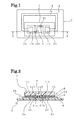
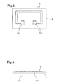
- [Fig. 1] A plan view of a non-contact ID card.
- [Fig. 2] A perspective cross section taken along the line X-X of Fig. 1.
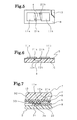
- [Fig. 3] A plan view of an antenna circuit board.
- [Fig. 4] A front elevational view of Fig. 3.
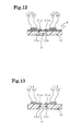
- [Fig. 5] A plan view of an interposer board.
- [Fig. 6] A longitudinal sectional view of Fig. 5.
- [Fig. 7] An enlarged view of an electrode bonding area of Fig. 2.
- [Fig. 8] A longitudinal sectional view for showing the positional relation between the antenna circuit board and the interposer board of Fig. 6 at the time of starting the bonding.
- [Fig. 9] A longitudinal sectional view for showing the state where the enlarged electrode of the interposer board of Fig. 6 is brought in contact with an insulating adhesive applied to the electrode (antenna electrode) of the antenna circuit board.
- [Fig. 10] A longitudinal sectional view for showing the state where the electrode (antenna electrode) of the antenna circuit board and the enlarged electrode of the interposer board of Fig. 6 are bonded.
- [Fig. 11] A longitudinal sectional view for showing another example of the interposer board.
- [Fig. 12] A longitudinal sectional view for showing another example of the interposer board.
- [Fig. 13] A longitudinal sectional view for showing another example of the interposer board.
- [Fig. 14] A longitudinal sectional view for showing the state where the electrode (antenna electrode) of the antenna circuit board and the enlarged electrode of the interposer board of Fig. 12 are bonded.
- [Fig. 15] An enlarged view of the electrode bonding area of Fig. 14.
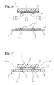
- [Fig. 16] A longitudinal sectional view for showing the positional relation between the antenna circuit board and the interposer board of Fig. 12 at the time of starting the bonding.
- [Fig. 17] A longitudinal sectional view for showing the state where the enlarged electrode of the interposer board of Fig. 12 is brought in contact with an insulating adhesive applied to the electrode (antenna electrode) of the antenna circuit board.
- The non-contact ID card according to the present invention is constructed by laminating an antenna circuit board and an interposer board. One of the examples is illustrated in a plan view of Fig. 1 and in Fig. 2 that is a perspective cross section taken along the line X-X of Fig. 1.
- In both drawings, an
interposer board 7 is laminated on anantenna circuit board 2 on the lower side. As shown in a plan view of Fig. 3 and in Fig. 4 that is a front elevational view of Fig.3, theantenna circuit board 2 has a structure in which anantenna 6 andelectrodes 3a and 3b (referred to as antenna electrodes hereinafter) connected thereto are formed on arectangular substrate 9 composed of a resin film which is an insulating material. - The
antenna 6 and theantenna electrodes 3a and 3b are formed by printing a conductive adhesive, a mixture of conductive particulates and resin binder, on a resin film and then drying or curing it. That is, as shown in the drawings, theantenna electrodes 3a and 3b are single layer resin electrodes. - Furthermore, it is possible to form the
antenna 6 and theantenna electrodes 3a and 3b described above by etching an aluminum foil or a copper foil that is stuck to a resin film. The electrodes in this case are metal electrodes. - Meanwhile, as shown in a plan view of Fig. 5 and in Fig. 6 that is a longitudinal sectional view of Fig. 5, the
interposer board 7 has a structure in which anIC chip 4 is embedded in arectangular substrate 10 composed of a resin film of an insulating material. That is, theIC chip 4 is embedded in thesubstrate 10 in such a manner that the circuit face of theIC chip 4 and the top face of thesubstrate 10 form the same plain face, andenlarged electrodes 11a and 11b connected to electrodes 12a and 12b of theIC chip 4 are also formed. - The
enlarged electrodes 11a and 11b are formed on an insulatingresin layer 8 formed on thesubstrate 10. Via connectingterminals enlarged electrodes 11a and 11b are connected to the electrodes 12a and 12b of theIC chip 4. - The
enlarged electrodes 11a and 11b and the connecting terminal 21a and 21b are formed by forming the via-hole in the insulating resin layer, printing and filling the conductive adhesive that is a mixture of the conductive particulates and the resin binder in the via-hole, and then drying or curing it. - Like the above-mentioned
antenna electrodes 3a and 3b, the enlargedelectrodes 11a and 11b are also single layer resin electrodes formed by using the conductive adhesive that is a mixture of the conductive particulates and the resin binder. - As shown in Fig. 1 and Fig. 2, both
antenna electrodes 3a and 3b and the enlargedelectrodes 11a and 11b are formed in a flat shape. As for the flat electrodes, it is possible to perform bonding as in such a manner of laminating web materials at the time of adhesively bonding both electrodes; thus, high-speed bonding can easily be achieved. Furthermore, the above-mentionedantenna electrodes 3a and 3b and theenlarged electrodes 11a and 11b are partially adhesively bonded in such a manner that each of the bonding faces is closely contacted to each other. Fig. 7 shows an enlarged view of the bonded state of the antenna electrode 3a and the enlarged electrode 11a. Bonding of theantenna electrode 3b and theenlarged electrode 11b that is not shown in the drawing is also the same. - The
antenna circuit board 2 and theinterposer board 7 are both substantially the flat substrates in a film form or a sheet form. Thus, the adhesive-bonding of theantenna circuit board 2 and theinterposer board 7 can be performed as if web materials such as a film-form material and a sheet form material are laminated and pasted. Therefore, the adhesive-bonding can be effectively performed. - As shown in the drawing, the antenna electrode 3a and the enlarged electrode 11a are adhesively bonded by an insulating
adhesive 33 that is filled in minute recesses 31 and 32, which are formed on each bonding face. Therecesses recesses - In a flip chip bonding of a semiconductor chip, so-called an NCP bonding method is well known, in which insulating resin is applied to the electrode of the substrate, the bump of the semiconductor chip is abutted against the substrate electrode and pressurized and heated, and the bonding is performed by using the shrinkage stress caused when the insulating resin is cured for bonding an electrode projection (bump) formed on an electrode of the semiconductor chip to an electrode of a circuit board. However, the NCP bonding method uses the bumps which are regularly arranged through complicated bump-forming steps such as photolithography and a lift-off method, whereas the electrodes of the present invention are naturally formed by printing the conductive adhesive which is a mixture of the conductive particulates and the resin binder and drying or curing it. Therefore, the electrode bumps (the minute convex portions in the present invention) for bonding can be formed easily at a low cost.
- When the insulating
adhesive 33 is used for bonding the above-mentionedantenna electrodes 3a and 3b and theenlarged electrodes 11a and 11b, it is possible that both electrodes conduct electricity by closely contacting the portions (a part of the bonding faces) on which therecesses adhesive 33 filled in therecesses recesses - The minute recesses 31 and 32 mentioned above are not limited to be formed only on the resin electrodes but also formed on the metal electrodes. Thus, the
antenna electrodes 3a and 3b and theenlarged electrodes 11a and 11b may be any electrodes selected from the metal electrodes, the resin electrodes, and the electrodes obtained by laminating the metal electrode and the resin electrode. - However, it is preferable that at least either one to be the resin electrode since
larger recesses - Examples of the above-mentioned conductive particulates are silver particles, particles obtained by performing silver-plating on copper particles, a mixture obtained by mixing carbon and silver particles, and so forth. Resin binder may be either thermoplastic or thermoset. The thermoplastic characteristic or the thermosetting characteristic is determined in accordance with the selection of the binder.
- The resin binder obtained by mixing the thermoplastic resin and the thermosetting resin may also be used. Examples of the thermoplastic resin are polyester-based resin, acryl-based resin, and so forth, and examples of the thermosetting resin are epoxy-based resin, polyimide-based resin, and so forth.
- The conductive adhesive of the above-mentioned composition is in a paste form, which is applied (for example, dropped, printed or the like) for forming the
antenna electrodes 3a and 3b, or theenlarged electrodes 11a and 11b, or both electrodes for the resin electrodes. The thermoplastic conductive adhesive is more preferable than the thermosetting conductive adhesive since it enables to shorten the processing time after applied. - It is also preferable to use a conductive adhesive obtained by mixing conductive particulates with the thermoplastic resin binder, with the resin binder obtained by mixing the thermoplastic resin and the thermosetting resin, or with other resin binder which, like the thermoplastic resin binder, exhibits the bonding property or the adhesion property when heated.
- In the case where the thermoplastic conductive adhesive is diluted in solvent to be printed, e.g. screen-printed, for forming the
enlarged electrodes 11a and 11b, theantenna electrodes 3a and 3b, or both electrodes, the electrodes are dried after the printing, and are subsequently bonded. It is the same in the case of using the thermosetting conductive adhesive. The thermosetting conductive adhesive exhibits a strong bonding strength; however, the processing time (thermosetting time) after the printing is relatively long (generally, several seconds or more). Thus, both may be used selectively in accordance with the reliability of the electrical properties and the like required in the non-contact ID card. - Adhesive-bonding of both electrodes are performed by laminating the
antenna circuit board 2 and theinterposer board 7 in the state where the positions of theantenna electrodes 3a and 3b and theenlarged electrodes 11a and 11b are aligned. Before that, the insulatingadhesive 33 is applied to either one of theantenna electrodes 3a and 3b or theenlarged electrodes 11a and 11b, or on both, so as to fill insulating adhesive into the minute recesses dispersed on the electrode bonding faces. Then, after the lamination, both electrodes are pressurized to be closely contacted to each other thereby bonding both electrodes together by the insulatingadhesive 33 filled in the minute recesses 31 and 32. - Another adhesive-bonding of both electrodes is performed by laminating the
antenna circuit board 2 and theinterposer board 7 in the state where the positions of theantenna electrodes 3a and 3b and theenlarged electrodes 11a and 11b are aligned. Before that, the insulatingadhesive 33. is applied to either one of theantenna electrodes 3a and 3b or theenlarged electrodes 11a and 11b, or on both. Then, after the lamination, both electrodes are pressurized and heated to be closely contacted to each other for filling the insulatingadhesive 33 into the minute recesses 31 and 32 dispersed on the respective bonding faces of both electrodes and squeezing out the remainder of the insulatingadhesive 33 from the closely contacted portion to the electrode side periphery. Thereby, both electrodes are bonded together by the insulatingadhesive 33 filled in the minute recesses 31 and 32. - It is possible to completely fill the minute recesses with the insulating
adhesive 33 by pressurizing and heating. By applying the insulatingadhesive 33 on the electrodes and filling it into the minute recesses before the bonding in lamination, both electrodes can be bonded together only by the above-described pressurization. Thus, a heating device becomes unnecessary and the apparatus is simplified. Moreover, it is possible to achieve high-speed lamination-bonding thereby enabling to improve the productivity. - Furthermore, in order to increase the reliability of the bonding while protecting the electrodes, the insulating
adhesive 33 with a sealing function (for example, a waterproof property or the like) can be used. In that case, for bonding both electrodes together, when the insulatingadhesive 33 is squeezed out to the electrode side periphery by pressurizing and heating for setting it around the electrodes, the electrode areas can be sealed. Thereby, the reliability of the electrical bonding in the bonding areas can be increased. - The insulating
adhesive 33 is not limited only to those with the bonding characteristic in addition to the insulating characteristic. It also includes so-called insulating pressure-sensitive adhesive with the pressure-sensitive adhesion characteristic in addition to the insulating characteristic. Preferred is the one that still keeps the adhesiveness even when cooled. Typical examples are hot-melt adhesives of EVA base, polyolefin base, synthetic rubber base, adhesive polymer base, urethane base reactive base, and so forth. The hot-melt adhesive has a characteristic that it easily spreads to form a thin layer when heated and pressurized. - Among those, the synthetic rubber hot-melt adhesive is most preferable since it has a characteristic of easily spreading to form a thinner layer even by a low pressurizing force. Application of the insulating
adhesive 33 for either one of theantenna electrodes 3a and 3b or theenlarged electrodes 11a and 11b may be performed by a conventionally known method, such as dropping by a nozzle and transferring by a pin or a roller. - When applying the insulating
adhesive 33 on the electrodes in advance, it is possible to fill it sufficiently into the depths of the minute recesses by applying it by a method of dropping, transferring, or the like after heating it so that it easily flows. Thus, if the insulatingadhesive 33 is heated and applied to the minute recesses in advance, it is possible to bond both electrodes only by pressurizing as in the above-described case. - The above-described adhesive-bonding will be described more specifically by referring to Fig. 8 to Fig. 10. Fig. 8 illustrates the state in which the
antenna circuit board 2 on the lower side and theinterposer board 7 on the upper side are laminated, and the insulatingadhesive 33 is applied to theantenna electrodes 3a and 3b on the lower side. In the meantime, positions of theenlarged electrodes 11a and 11b on the upper side are aligned to be appropriate for bonding with theantenna electrodes 3a and 3b. - Fig. 9 illustrates the laminated state in which the
interposer board 7 is brought down and theenlarged electrodes 11a and 11b are in contact with the insulatingadhesive 33 on theantenna electrodes 3a and 3b. Furthermore, Fig. 10 illustrates the state in which both electrodes are closely contacted to each other by heating and pressurizing theinterposer board 7 against theantenna circuit board 2. In other words, theenlarged electrodes 11a and 11b and theantenna electrodes 3a and 3b are closely contacted to each other. - This heating and pressurization is performed by using a heat tool, which is not shown. By pressurizing and heating to closely contact both electrodes to each other, the insulating
adhesive 33 can be filled in the minute recesses 31 and 32 (see Fig. 7) dispersed on the respective bonding faces of both electrodes, as described above. Moreover, the remainder of the insulatingadhesive 33 can be squeezed out from the closely contacted portion to the electrode side periphery so that both electrodes can be adhesively bonded together by the insulatingadhesive 33 filled in the minute recesses 31 and 32. When the above-mentioned hot-melt adhesive is selected as the insulatingadhesive 33, it is possible to lamination-bond both boards in an extremely short time of about 0.05 to 0.2 seconds. - In the present invention, the
interposer board 7 may be the one in Fig. 11 instead of the one in Fig. 6 described above. TheIC chip 4 is embedded in thesubstrate 10 in these figures; however, it may be mounted without embedding theIC chip 4. However, it is preferable to embed theIC chip 4 in thesubstrate 10 for achieving a thinner board. - By using the web-type interposer board in which the
IC chip 4 is embedded in the resin film, and the web-type antenna circuit board formed also by the resin film and the like, it is possible to bond both electrodes in lamination by a roll-to-roll method in the manner for commonly handling the web-type substance, and to manufacture the non-contact ID card. - Furthermore, as described above, at least either one of the
antenna electrodes 3a and 3b or theenlarged electrodes 11a and 11b may be formed to be the laminated electrode comprising layers of the resin electrodes formed by using a plurality of conductive adhesives of various compositions, instead of being formed to be the single layer electrode comprising the resin electrode. For example, it may be the laminated electrode obtained by forming the upper layer electrode formed by using the thermoplastic conductive adhesive on the lower layer electrode formed by using a thermosetting conductive adhesive. - Furthermore, as shown in Fig. 12 and Fig. 13, the
enlarged electrodes 11a and 11b may be formed of the laminated electrodes and comprise layers of ametal electrode 35 formed on thesubstrate 10 and aresin electrode 36 that is formed on themetal electrode 35 by using a conductive adhesive. Theinterposer board 7 in Fig. 12 comprises an insulatingresin layer 8, but theinterposer board 7 in Fig. 13 does not. - As shown in Fig. 14, the
interposer board 7 and theantenna circuit board 2 shown in Fig. 12 can be bonded. In this case, theantenna electrodes 3a and 3b and theenlarged electrodes 11a and 11b are also adhesively bonded in the state in which the respective bonding faces are closely contacted to each other. Fig. 15 illustrates the enlarged view of the bonded state of one of the antenna electrode 3a and the enlarged electrode 11a. The bonding of theother antenna electrode 3b and theenlarged electrode 11b, which is not shown, is also the same. - As shown in the drawing, the antenna electrode 3a and the enlarged electrode 11a are adhesively bonded by the insulating
adhesive 33 filled in the minute recesses 31 and 32, which are formed on the respective bonding faces. The bonding face of the enlarged electrode 11a is formed by using the above-mentionedresin electrode 36, and the insulatingadhesive 33 is filled in theminute recess 32 dispersed thereon. In Fig. 15, therecesses - Thus, by the insulating
adhesive 33, it is possible that both electrodes conduct electricity by closely contacting the portions (a part of the bonding faces) to each other where therecesses adhesive 33 filled in therecesses - For this bonding, as shown in Fig. 16, the insulating
adhesive 33 is applied to theantenna electrodes 3a and 3b on the lower side. In the meantime, the positions of theenlarged electrodes 11a and 11b on the upper side are aligned to be appropriate for being bonded to theantenna electrodes 3a and 3b. Then, as shown in Fig. 17, theinterposer board 7 is brought down to be laminated in the state in which theenlarged electrodes 11a and 11b are in contact with the insulatingadhesive 33 on theantenna electrodes 3a and 3b. Then, theinterposer board 7 is heated and pressurized against theantenna circuit board 2 to closely contact both electrodes to each other. Therefore, as described above, both electrodes can be securely adhesive-bonded. - Fig. 16 illustrates the case in which the insulating
adhesive 33 is applied to theantenna electrodes 3a and 3b. However, before the bonding, if the insulatingadhesive 33 is applied in advance to theenlarged electrodes 11a and 11b, and is filled in the minute recesses, it is possible to align the positions of the enlarged electrodes with respect to the antenna electrodes and to perform the bonding with electrical conductivity by pressurization. - Instead of forming the
enlarged electrodes 11a and 11b by the laminated electrode comprising layers of themetal electrode 35 formed on thesubstrate 10 and theresin electrode 36 formed on themetal electrode 35 by using the conductive adhesive, it is possible to form only theantenna electrodes 3a and 3b, or bothenlarged electrodes 11a and 11b and theantenna electrodes 3a and 3b, as the laminated electrode that is constituted of themetal electrode 35 and theresin electrode 36. In short, at least either of theantenna electrodes 3a and 3b or theenlarged electrodes 11a and 11b may be formed to be such laminated electrode. - When the
enlarged electrodes 11a and 11b were formed with themetal electrode 35 and theresin electrode 36 that was formed by using the thermoplastic conductive adhesive so as to be bonded to theantenna electrodes 3a and 3b of the metal electrode, the bonding was achieved in 0.05 to 0.2 seconds. The electric resistance value in the bonding area at that time was 0.1 Ω to 1Ω, and the bonding strength was 10N/cm to 50N/cm. - In the case of using the conductive adhesive obtained by mixing the conductive particulates with the resin binder of a mixture of the thermoplastic resin and the thermosetting resin, or with other resin binder which, like the thermoplastic resin binder, exhibits the bonding property or the adhesion property when heated, the bonding time and the electric resistance value were almost the same. A rotary-type composed of a pressure roller comprised of a heat source is preferable as a heat tool to be used as a means for heating and pressurizing at the time of bonding. Particularly, it is preferable to arrange a plurality of rotary-type heat tools in series for heating and pressurizing the laminated body of the antenna circuit board and the interposer board by these heat tools. This is because high-speed bonding can be achieved by shortening the bonding time.
- It is preferable that the insulating adhesive used for adhesive-bonding is expanded thin to be spread at a low temperature by a small pressurizing force and also in a short time. Therefore, the relation between the tensile strength and the elongation of the insulating adhesive is important. The tensile strength is 3 MPa or less, and preferable to be 1 MPa or less. The elongation is 300 % or more, and preferable to be 500 % or more.
- Antenna resin electrode were formed on a polyester film by a printing method using thermoplastic silver paste FA-333, a product of Fujikura Ltd. The antenna resin electrode is 2.0 mm x 2.0 mm in size and 12 µm in thickness. Meanwhile, enlarged resin electrode were formed by the same printing method using thermoplastic silver paste PES-E91, a product of TOAGOSEI CO., LTD. The enlarged resin electrode is 2.5 mm x 2.5 mm in size and 30 µm in thickness.
- For adhesively bonding the enlarged resin electrodes and the antenna resin electrodes, a synthetic rubber hot-melt agent PPET, a product of TOAGOSEI CO., LTD, was applied to the antenna electrode by 0.5 mg per electrode using a transfer pin. Then, the interposer board was adsorbed by a vacuum suction port of a pressurizing tool for aligning the positions of the antenna resin electrodes and the enlarged electrodes. Subsequently, the pressurizing tool was brought down for pressurizing and heating both electrodes to achieve adhesive-bonding.
- The heating temperature at that time was at 180 °C, the pressurizing force was 0.8 MPa, and the adhesive-bonding time was 0.2 seconds. The bonding resistance at that time was 0.3 to 0.4 Ω. The increase of the resistance value was within the permissible range even after going through a high-temperature/high-humidity test at 60 °C and 93 %RH and a temperature cycle test run between -40 °C and 80 °C.
- The PPET used for the adhesive-bonding was an insulating adhesive having an extremely stretchable characteristic with the tensile strength of 0.3 MPa and the elongation of 1400 %.
Claims (14)
- A non-contact ID card, comprising an antenna circuit board having an antenna formed on a substrate, and an interposer board having an enlarged electrode, which is connected to an electrode of an IC chip, formed on a substrate on which the IC chip is mounted; the non-contact ID card being formed by laminating both boards in such a manner that an electrode of the antenna and the enlarged electrode are bonded, wherein
both electrodes are adhesively bonded by an insulating adhesive filled in minute recesses dispersed on bonding faces of the electrode of the antenna and/or the enlarged electrode. - The non-contact ID card as claimed in claim 1, wherein at least either of the electrode of the antenna and the enlarged electrode is a single layer electrode comprising a resin electrode which is formed by using a conductive adhesive.
- The non-contact ID card as claimed in claim 1, wherein at least either of the electrode of the antenna and the enlarged electrode is a laminated electrode comprising layers of resin electrodes which are formed by using a plurality of conductive adhesives of various compositions.
- The non-contact ID card as claimed in claim 1, wherein at least either of the electrode of the antenna and the enlarged electrode is a laminated electrode comprising layers of a metal electrode that is formed on the substrate and a resin electrode that is formed by using a conductive adhesive on the metal electrode.
- The non-contact ID card as claimed in claim 2, 3, or 4, wherein the conductive adhesive is thermoplastic.
- The non-contact ID card as claimed in claim 2, 3, or 4, wherein the conductive adhesive is thermoset.
- The non-contact ID card as claimed in any one of claims 1 to 6, wherein the IC chip is embedded in the substrate.
- A manufacturing method of a non-contact ID card, comprising the steps of;
laminating an antenna circuit board having an antenna formed on a substrate and an interposer board having an enlarged electrode, which is connected to an electrode of an IC chip, formed on a substrate on which the IC chip is mounted in such a manner that positions of an electrode of the antenna and the enlarged electrode align
applying an insulating adhesive, prior to the laminating process, on at least either of the electrode of the antenna and the enlarged electrode so as to fill insulating adhesive into minute recesses dispersed on a bonding face of the respective electrode, and
pressurizing to tightly make both electrodes contact with each other, and after the laminating process, so that both electrodes are adhesively bonded to each other by the insulating adhesive filled in the minute recesses. - A manufacturing method of a non-contact ID card, comprising the steps of;
laminating an antenna circuit board having an antenna formed on a substrate and an interposer board having an enlarged electrode, which is connected to an electrode of an IC chip, formed on a substrate on which the IC chip is mounted in such a manner that positions of an electrode of the antenna and the enlarged electrode align
applying an insulating adhesive, prior to the laminating process, on at least either of the electrode of the antenna and the enlarged electrode, and
pressurizing and heating to tightly make both electrodes contact with each other, after the laminating process, so that the insulating adhesive is filled into the minute recesses dispersed on at least either bonding face of both electrodes, the remainder of the insulating adhesive is squeezed from the close contact portion of the electrodes to the side periphery of the electrodes, and both electrodes are adhesively bonded to each other by the insulating adhesive filled in the minute recesses. - The manufacturing method of the non-contact ID card as claimed in claim 9, wherein the step of pressurizing and heating is held by a heat tool.
- The manufacturing method of the non-contact ID card as claimed in claim 8, 9, or 10, wherein at least either of the electrode of the antenna and the enlarged electrode is a single layer electrode comprising a resin electrode which is formed by using a conductive adhesive.
- The manufacturing method of the non-contact ID card as claimed in claim 8, 9, or 10, wherein at least either of the electrode of the antenna and the enlarged electrode is a laminated electrode comprising layers of resin electrodes which are formed by using a plurality of conductive adhesives of various compositions.
- The manufacturing method of the non-contact ID card as claimed in claim 8, 9, or 10, wherein at least either of the electrode of the antenna and the enlarged electrode is a laminated electrode comprising layers of a metal electrode that is formed on the substrate and a resin electrode that is formed by using a conductive adhesive on the metal electrode.
- The manufacturing method of the non-contact ID card as claimed in any one of claims 8 to 13, wherein the IC chip is embedded in the substrate.
Applications Claiming Priority (2)
| Application Number | Priority Date | Filing Date | Title |
|---|---|---|---|
| JP2003380645 | 2003-11-11 | ||
| PCT/JP2004/016564 WO2005045919A1 (en) | 2003-11-11 | 2004-11-09 | Non-contact id card and manufacturing method thereof |
Publications (1)
| Publication Number | Publication Date |
|---|---|
| EP1684338A1 true EP1684338A1 (en) | 2006-07-26 |
Family
ID=34567246
Family Applications (1)
| Application Number | Title | Priority Date | Filing Date |
|---|---|---|---|
| EP04799541A Withdrawn EP1684338A1 (en) | 2003-11-11 | 2004-11-09 | Non-contact id card and manufacturing method thereof |
Country Status (7)
| Country | Link |
|---|---|
| US (1) | US7332798B2 (en) |
| EP (1) | EP1684338A1 (en) |
| JP (1) | JPWO2005045919A1 (en) |
| KR (1) | KR20060100199A (en) |
| CN (1) | CN1784776A (en) |
| TW (1) | TWI274369B (en) |
| WO (1) | WO2005045919A1 (en) |
Cited By (2)
| Publication number | Priority date | Publication date | Assignee | Title |
|---|---|---|---|---|
| US8404525B2 (en) | 2006-01-10 | 2013-03-26 | Semiconductor Energy Laboratory Co., Ltd. | Semiconductor device, manufacturing method of semiconductor device, and RFID tag |
| EP3322264A4 (en) * | 2015-07-08 | 2019-03-06 | Alps Electric Co., Ltd. | High frequency module |
Families Citing this family (7)
| Publication number | Priority date | Publication date | Assignee | Title |
|---|---|---|---|---|
| JP5057767B2 (en) * | 2006-01-10 | 2012-10-24 | 株式会社半導体エネルギー研究所 | Method for manufacturing semiconductor device |
| KR101237107B1 (en) | 2007-09-14 | 2013-02-25 | 도판 인사츠 가부시키가이샤 | Antenna sheet, transponder and book form |
| WO2010088556A1 (en) * | 2009-01-30 | 2010-08-05 | Datakey Electronics, Inc. | Data carrier system having a compact footprint and methods of manufacturing the same |
| JP5473017B2 (en) * | 2011-12-12 | 2014-04-16 | コヴィオ インコーポレイテッド | RF tag / device and / or RFID tag / device having an integrated interposer, and methods for making and using the same |
| CN104143690A (en) * | 2014-07-31 | 2014-11-12 | 清华大学深圳研究生院 | Manufacturing method for antenna |
| CN110239082A (en) * | 2019-05-14 | 2019-09-17 | 山东理工大学 | A composite processing method of plastic material 3D printing and milling |
| US11540578B2 (en) | 2020-03-12 | 2023-01-03 | Matscitechno Licensing Company | Helmet system |
Family Cites Families (12)
| Publication number | Priority date | Publication date | Assignee | Title |
|---|---|---|---|---|
| JPH0682706B2 (en) * | 1986-05-29 | 1994-10-19 | 松下電器産業株式会社 | Connection |
| JPH0815154B2 (en) | 1987-05-15 | 1996-02-14 | 松下電器産業株式会社 | Bump for semiconductor element |
| JPH02101753A (en) | 1988-10-11 | 1990-04-13 | Hitachi Chem Co Ltd | Semiconductor chip attached structure |
| JPH0513419A (en) | 1991-07-03 | 1993-01-22 | Rohm Co Ltd | Method for forming bump portion of semiconductor element |
| JPH06177214A (en) * | 1992-05-13 | 1994-06-24 | Fujitsu Ltd | Crimp terminal and connecting method therefor and mounting method for semiconductor device |
| JP3333300B2 (en) * | 1993-01-28 | 2002-10-15 | 松下電器産業株式会社 | Method for forming bumps having uneven surface, method for mounting semiconductor device having bumps, and semiconductor unit |
| JP3135435B2 (en) * | 1993-10-19 | 2001-02-13 | 松下電器産業株式会社 | Circuit board electrode connection method |
| JPH10313161A (en) | 1997-05-12 | 1998-11-24 | Hitachi Chem Co Ltd | Wiring board |
| JP4240670B2 (en) | 1999-08-31 | 2009-03-18 | 三菱重工業株式会社 | Method and apparatus for forming ribbed plate |
| JP2001217281A (en) | 2000-01-31 | 2001-08-10 | Matsushita Electric Ind Co Ltd | Semiconductor device and manufacturing method thereof |
| EP1258370B1 (en) * | 2000-02-22 | 2008-12-24 | Toray Engineering Co., Ltd. | Noncontact id card and method of manufacturing the same |
| JP3478281B2 (en) * | 2001-06-07 | 2003-12-15 | ソニー株式会社 | IC card |
-
2004
- 2004-11-09 JP JP2005515344A patent/JPWO2005045919A1/en active Pending
- 2004-11-09 WO PCT/JP2004/016564 patent/WO2005045919A1/en not_active Ceased
- 2004-11-09 US US10/553,460 patent/US7332798B2/en not_active Expired - Fee Related
- 2004-11-09 KR KR1020057020405A patent/KR20060100199A/en not_active Withdrawn
- 2004-11-09 CN CNA2004800124704A patent/CN1784776A/en active Pending
- 2004-11-09 EP EP04799541A patent/EP1684338A1/en not_active Withdrawn
- 2004-11-11 TW TW093134397A patent/TWI274369B/en not_active IP Right Cessation
Non-Patent Citations (1)
| Title |
|---|
| See references of WO2005045919A1 * |
Cited By (2)
| Publication number | Priority date | Publication date | Assignee | Title |
|---|---|---|---|---|
| US8404525B2 (en) | 2006-01-10 | 2013-03-26 | Semiconductor Energy Laboratory Co., Ltd. | Semiconductor device, manufacturing method of semiconductor device, and RFID tag |
| EP3322264A4 (en) * | 2015-07-08 | 2019-03-06 | Alps Electric Co., Ltd. | High frequency module |
Also Published As
| Publication number | Publication date |
|---|---|
| TW200523994A (en) | 2005-07-16 |
| KR20060100199A (en) | 2006-09-20 |
| CN1784776A (en) | 2006-06-07 |
| US7332798B2 (en) | 2008-02-19 |
| WO2005045919A1 (en) | 2005-05-19 |
| US20060279941A1 (en) | 2006-12-14 |
| TWI274369B (en) | 2007-02-21 |
| JPWO2005045919A1 (en) | 2007-05-24 |
Similar Documents
| Publication | Publication Date | Title |
|---|---|---|
| KR100732648B1 (en) | Contactless ID card and its manufacturing method | |
| JP3894540B2 (en) | Interposer with conductive connection | |
| JP4663184B2 (en) | Manufacturing method of semiconductor device | |
| US20040183182A1 (en) | Apparatus incorporating small-feature-size and large-feature-size components and method for making same | |
| US20040037053A1 (en) | Noncontact ID card and method of manufacturing the same | |
| TWI863970B (en) | Method for manufacturing connection structure the manufacturing connection, film structure body and method for manufacturing the film structure body | |
| TWI284844B (en) | Noncontact ID card or the like and method of manufacturing the same | |
| US7332798B2 (en) | Non-contact ID card and manufacturing method thereof | |
| JP3822043B2 (en) | Chip part assembly manufacturing method | |
| US8695207B2 (en) | Method for manufacturing an electronic device | |
| JP2000286299A (en) | Semiconductor device connection method | |
| JP4515129B2 (en) | Manufacturing method of semiconductor device | |
| MX2008012339A (en) | Methods for attaching a flip chip integrated circuit assembly to a substrate. | |
| JP2011199138A (en) | Method and structure for connection between electronic component | |
| JP2011077125A (en) | Wiring board, manufacturing method of wiring board, connection structure of wiring board, and connection method of wiring board | |
| CN107424966B (en) | A kind of structure and method of crystal covered chip and flexible base plate encapsulation | |
| JPH08320498A (en) | Terminal connecting structure of liquid crystal display panel | |
| KR20110118582A (en) | Manufacturing method of semiconductor chip | |
| JP3881195B2 (en) | Manufacturing method of semiconductor component mounted component, semiconductor component mounted component, manufacturing method of semiconductor component mounted finished product, and semiconductor component mounted finished product | |
| JP2004086852A (en) | Non-contact id card or the like, and its manufacturing method | |
| JP2004062634A (en) | Non-contact communication medium joining method and non-contact communication medium | |
| JP2003124258A (en) | Semiconductor chip mounting method and semiconductor chip mounting structure | |
| JP2008078280A (en) | Method for manufacturing electronic circuit element | |
| TW200839985A (en) | Method for disposing conductive particles on contacts of a substrate | |
| JP2003163432A (en) | Conductive connection formed on adhesive sheet |
Legal Events
| Date | Code | Title | Description |
|---|---|---|---|
| PUAI | Public reference made under article 153(3) epc to a published international application that has entered the european phase |
Free format text: ORIGINAL CODE: 0009012 |
|
| 17P | Request for examination filed |
Effective date: 20051024 |
|
| AK | Designated contracting states |
Kind code of ref document: A1 Designated state(s): DE FR GB |
|
| DAX | Request for extension of the european patent (deleted) | ||
| RBV | Designated contracting states (corrected) |
Designated state(s): DE FR GB |
|
| 18D | Application deemed to be withdrawn |
Effective date: 20080603 |
|
| STAA | Information on the status of an ep patent application or granted ep patent |
Free format text: STATUS: THE APPLICATION IS DEEMED TO BE WITHDRAWN |
|
| R18D | Application deemed to be withdrawn (corrected) |
Effective date: 20080603 |