EP1680818B1 - Light-emitting diode arrangement comprising a heat-dissipating plate - Google Patents
Light-emitting diode arrangement comprising a heat-dissipating plate Download PDFInfo
- Publication number
- EP1680818B1 EP1680818B1 EP04818383.4A EP04818383A EP1680818B1 EP 1680818 B1 EP1680818 B1 EP 1680818B1 EP 04818383 A EP04818383 A EP 04818383A EP 1680818 B1 EP1680818 B1 EP 1680818B1
- Authority
- EP
- European Patent Office
- Prior art keywords
- light
- emitting diode
- diode chip
- arrangement according
- plate
- Prior art date
- Legal status (The legal status is an assumption and is not a legal conclusion. Google has not performed a legal analysis and makes no representation as to the accuracy of the status listed.)
- Expired - Lifetime
Links
- 229910052751 metal Inorganic materials 0.000 claims description 16
- 239000002184 metal Substances 0.000 claims description 16
- 239000000463 material Substances 0.000 claims description 15
- 239000000758 substrate Substances 0.000 claims description 12
- 238000006243 chemical reaction Methods 0.000 claims description 9
- 239000000853 adhesive Substances 0.000 claims description 5
- 230000001070 adhesive effect Effects 0.000 claims description 5
- 230000017525 heat dissipation Effects 0.000 claims description 5
- 239000002313 adhesive film Substances 0.000 claims description 3
- 229910017083 AlN Inorganic materials 0.000 claims 1
- PIGFYZPCRLYGLF-UHFFFAOYSA-N Aluminum nitride Chemical compound [Al]#N PIGFYZPCRLYGLF-UHFFFAOYSA-N 0.000 claims 1
- 239000010410 layer Substances 0.000 description 26
- 239000004020 conductor Substances 0.000 description 7
- 230000000694 effects Effects 0.000 description 7
- 239000000126 substance Substances 0.000 description 6
- 239000000919 ceramic Substances 0.000 description 4
- PMHQVHHXPFUNSP-UHFFFAOYSA-M copper(1+);methylsulfanylmethane;bromide Chemical compound Br[Cu].CSC PMHQVHHXPFUNSP-UHFFFAOYSA-M 0.000 description 3
- 239000012790 adhesive layer Substances 0.000 description 2
- 230000004888 barrier function Effects 0.000 description 2
- 239000003822 epoxy resin Substances 0.000 description 2
- 238000009413 insulation Methods 0.000 description 2
- 230000004048 modification Effects 0.000 description 2
- 238000012986 modification Methods 0.000 description 2
- 229920000647 polyepoxide Polymers 0.000 description 2
- 239000004065 semiconductor Substances 0.000 description 2
- RYGMFSIKBFXOCR-UHFFFAOYSA-N Copper Chemical compound [Cu] RYGMFSIKBFXOCR-UHFFFAOYSA-N 0.000 description 1
- 239000004593 Epoxy Substances 0.000 description 1
- OAICVXFJPJFONN-UHFFFAOYSA-N Phosphorus Chemical compound [P] OAICVXFJPJFONN-UHFFFAOYSA-N 0.000 description 1
- 239000002390 adhesive tape Substances 0.000 description 1
- 229910052782 aluminium Inorganic materials 0.000 description 1
- XAGFODPZIPBFFR-UHFFFAOYSA-N aluminium Chemical compound [Al] XAGFODPZIPBFFR-UHFFFAOYSA-N 0.000 description 1
- 238000003491 array Methods 0.000 description 1
- 239000010953 base metal Substances 0.000 description 1
- 239000000969 carrier Substances 0.000 description 1
- 239000012876 carrier material Substances 0.000 description 1
- 229910010293 ceramic material Inorganic materials 0.000 description 1
- 239000012141 concentrate Substances 0.000 description 1
- 238000001816 cooling Methods 0.000 description 1
- 229910052802 copper Inorganic materials 0.000 description 1
- 239000010949 copper Substances 0.000 description 1
- 230000006378 damage Effects 0.000 description 1
- 230000001419 dependent effect Effects 0.000 description 1
- 230000007613 environmental effect Effects 0.000 description 1
- 239000000945 filler Substances 0.000 description 1
- 238000010438 heat treatment Methods 0.000 description 1
- 238000009434 installation Methods 0.000 description 1
- 238000002955 isolation Methods 0.000 description 1
- 150000002739 metals Chemical class 0.000 description 1
- 238000000034 method Methods 0.000 description 1
- 230000007935 neutral effect Effects 0.000 description 1
- 239000011368 organic material Substances 0.000 description 1
- 229910052594 sapphire Inorganic materials 0.000 description 1
- 239000010980 sapphire Substances 0.000 description 1
Images

Classifications
-
- H01L33/64—
-
- H—ELECTRICITY
- H01—ELECTRIC ELEMENTS
- H01L—SEMICONDUCTOR DEVICES NOT COVERED BY CLASS H10
- H01L2224/00—Indexing scheme for arrangements for connecting or disconnecting semiconductor or solid-state bodies and methods related thereto as covered by H01L24/00
- H01L2224/01—Means for bonding being attached to, or being formed on, the surface to be connected, e.g. chip-to-package, die-attach, "first-level" interconnects; Manufacturing methods related thereto
- H01L2224/10—Bump connectors; Manufacturing methods related thereto
- H01L2224/15—Structure, shape, material or disposition of the bump connectors after the connecting process
- H01L2224/16—Structure, shape, material or disposition of the bump connectors after the connecting process of an individual bump connector
- H01L2224/161—Disposition
- H01L2224/16135—Disposition the bump connector connecting between different semiconductor or solid-state bodies, i.e. chip-to-chip
- H01L2224/16145—Disposition the bump connector connecting between different semiconductor or solid-state bodies, i.e. chip-to-chip the bodies being stacked
-
- H—ELECTRICITY
- H01—ELECTRIC ELEMENTS
- H01L—SEMICONDUCTOR DEVICES NOT COVERED BY CLASS H10
- H01L2224/00—Indexing scheme for arrangements for connecting or disconnecting semiconductor or solid-state bodies and methods related thereto as covered by H01L24/00
- H01L2224/01—Means for bonding being attached to, or being formed on, the surface to be connected, e.g. chip-to-package, die-attach, "first-level" interconnects; Manufacturing methods related thereto
- H01L2224/42—Wire connectors; Manufacturing methods related thereto
- H01L2224/47—Structure, shape, material or disposition of the wire connectors after the connecting process
- H01L2224/48—Structure, shape, material or disposition of the wire connectors after the connecting process of an individual wire connector
- H01L2224/4805—Shape
- H01L2224/4809—Loop shape
- H01L2224/48091—Arched
-
- H—ELECTRICITY
- H01—ELECTRIC ELEMENTS
- H01L—SEMICONDUCTOR DEVICES NOT COVERED BY CLASS H10
- H01L2224/00—Indexing scheme for arrangements for connecting or disconnecting semiconductor or solid-state bodies and methods related thereto as covered by H01L24/00
- H01L2224/73—Means for bonding being of different types provided for in two or more of groups H01L2224/10, H01L2224/18, H01L2224/26, H01L2224/34, H01L2224/42, H01L2224/50, H01L2224/63, H01L2224/71
- H01L2224/732—Location after the connecting process
- H01L2224/73251—Location after the connecting process on different surfaces
- H01L2224/73265—Layer and wire connectors
-
- H—ELECTRICITY
- H01—ELECTRIC ELEMENTS
- H01L—SEMICONDUCTOR DEVICES NOT COVERED BY CLASS H10
- H01L2224/00—Indexing scheme for arrangements for connecting or disconnecting semiconductor or solid-state bodies and methods related thereto as covered by H01L24/00
- H01L2224/80—Methods for connecting semiconductor or other solid state bodies using means for bonding being attached to, or being formed on, the surface to be connected
- H01L2224/85—Methods for connecting semiconductor or other solid state bodies using means for bonding being attached to, or being formed on, the surface to be connected using a wire connector
- H01L2224/85909—Post-treatment of the connector or wire bonding area
- H01L2224/8592—Applying permanent coating, e.g. protective coating
-
- H01L33/642—
-
- H—ELECTRICITY
- H05—ELECTRIC TECHNIQUES NOT OTHERWISE PROVIDED FOR
- H05K—PRINTED CIRCUITS; CASINGS OR CONSTRUCTIONAL DETAILS OF ELECTRIC APPARATUS; MANUFACTURE OF ASSEMBLAGES OF ELECTRICAL COMPONENTS
- H05K1/00—Printed circuits
- H05K1/02—Details
- H05K1/0201—Thermal arrangements, e.g. for cooling, heating or preventing overheating
- H05K1/0203—Cooling of mounted components
-
- H—ELECTRICITY
- H05—ELECTRIC TECHNIQUES NOT OTHERWISE PROVIDED FOR
- H05K—PRINTED CIRCUITS; CASINGS OR CONSTRUCTIONAL DETAILS OF ELECTRIC APPARATUS; MANUFACTURE OF ASSEMBLAGES OF ELECTRICAL COMPONENTS
- H05K1/00—Printed circuits
- H05K1/18—Printed circuits structurally associated with non-printed electric components
- H05K1/182—Printed circuits structurally associated with non-printed electric components associated with components mounted in the printed circuit board, e.g. insert mounted components [IMC]
Definitions
- the present invention relates to light-emitting diode arrays in which LED dice (light-emitting diode chips) are arranged on a heat dissipating board.
- the invention is to the effect that the heat loss can be dissipated by improving the thermal resistance of the device more efficient. If according to the invention, the heat can be dissipated well by low thermal resistance, it can be transferred without high temperature gradient on the LED carrier.
- the thermal resistance is expressed in K (Kelvin) / W (Watt).
- PCBs printed circuit boards
- ceramic boards are known, which, although better thermal properties compared to the printed circuit boards based on epoxy resin, but are very brittle and fragile, which more than limits their use as a carrier material.
- metal core boards are also used in the prior art. These typically have a sandwich-type structure based on the metal core base, an insulation layer and a conductor track.
- US Pat. No. 6,498,355 B1 describes a light emitting diode array comprising a light emitting diode chip and a multi-layer metal circuit board.
- the base is a core of the board and serves for heat dissipation.
- the light-emitting diode arrangement has an electrically insulating and thermally conductive connecting layer between an emitting surface of the light-emitting diode chip and the circuit board.
- an intermediate carrier is arranged between the light-emitting diode chip and the board.
- the invention is based on the recognition that the prior art in the use of metal core boards, the dissipation of heat loss from the LED, which is placed on the conductor, is limited by the underlying insulating layer, which in turn limits the power density of the LED.
- a light-emitting diode arrangement with at least one light-emitting diode chip is provided. Furthermore, a multilayer board comprising a base of a thermally highly conductive material, such as metal is provided, the base is a core of the board and is used for heat dissipation and wherein an electrically insulating and thermally conductive bonding layer between the emitting surface of the LED chip and the board is arranged.
- the light-emitting diode chip is arranged such that the substrate of the light-emitting diodes faces away from the printed circuit board, wherein an intermediate carrier separate from these parts is arranged between the light-emitting diode chip and the base of the printed circuit board, with which the light-emitting diode chip is electrically contacted the intermediate carrier is formed by an aluminum nitride substrate, wherein the electrically insulating connecting layer is an adhesive film, which is arranged directly on the base and on which the intermediate carrier is arranged directly Contrary to the prior art, the thermal insulating (epoxy) layer is eliminated, the heat transfer from the LED chip to the heat dissipating base material of the board is significantly improved.
- An insulating adhesive layer which is realized by an adhesive film, is particularly advantageous if a light-emitting diode chip is used, whose base-facing surface is electrically conductive. In this case, separate electrical isolation must be provided between the chip and the base to prevent short circuits and ESD failures.
- the light-emitting diode chip can be accommodated in a recess of the board.
- the light-emitting diode chip can be sunk in such a way that its upper side does not protrude beyond the contour of the board and, for example, terminates flush with the upper side of the board.
- the recess into which the LED chip is set can be formed in the heat-dissipating base of the board.
- the depression can have further functions.
- the recess may have a reflector effect, wherein advantageously the walls of the recess are at least partially bevelled.
- the light-emitting diode arrangement is formed by the "face-down" mounting technique, in which the light-emitting diode chip is arranged such that the substrate of the light-emitting diodes faces away from the circuit board.
- the light-emitting diode chip can be arranged on the intermediate carrier by means of a conductive adhesive.
- the side of the intermediate carrier facing the printed circuit board can be electrically insulating, wherein the region of the intermediate carrier facing the light-emitting diode chip can have conductive regions, such as conductor tracks.
- At least the region of the at least one light-emitting diode chip may be covered by a lens, such as a Fresnel lens.
- the area between the board and the lens may be at least partially filled with a color conversion substance.
- the color conversion substance can therefore be arranged next to and / or above the light-emitting diode chip.
- the recess can be filled laterally from the chip with a color conversion substance to obtain an LED with a substantially white light characteristic.
- the light-emitting diode chip can be contacted by means of wires from a printed circuit board, wherein this printed circuit board is laterally applied by the light-emitting diode chip sandwiched by means of an intermediate insulating layer on the board.
- an LED should be placed as directly as possible on the heat dissipating base, for example, a metal core board.
- this step must overcome the problem that LED dies are often conductive across the LED substrate or its base-facing surface, which can result in a short circuit to the printed circuit board base material, which is often undesirable and particularly so regarding the wiring options of the LEDs no design freedom.
- an LED die is placed on the base material (for example metal) 5 of a metal-core board 17 by means of a thermally conductive but electrically insulating layer 2.
- the metal core board 17 has, in addition to this base metal core 5, an overlying electrically insulating layer 4 and an electrically conductive layer with conductor tracks 3, wherein preferably the electrically insulating layer 4 and the interconnect layer 3 have congruent recesses 16, in which the LED die 1 is inserted.
- the electrical contacting of the LED dies occurs in this arrangement, in which the substrate of the LED dies facing the printed circuit board 1), laterally from the printed conductors 3 by means of wires 11 on the upper side of the LED dice.
- the region of the LED dies 1 and the recess 16 can be covered by a substantially dome-shaped lens 6, which concentrates the light emitted by the LED die 1.
- the electrical contacting of in FIG. 1 The LED arrangement shown can be made via plug contacts 7, etc. provided outside the area covered by the lens 6.
- a material with high thermal conductivity is generally used, so that preferably metals, such as aluminum or copper can be used.
- the electrically insulating but thermally conductive connection layer 2 can be, for example, a non-conductive substrate layer of the LEDs (for example, green LEDs often use sapphire) or else a thermally conductive and electrically insulating adhesive.
- the electrically insulating but thermally conductive connection layer 2 may therefore be part of the LED dies 1, the multilayer board 17 and / or a separate layer thereof.
- the separate Layer is particularly necessary when the LED Dies 1 are arranged such that their the multilayer board 17 facing surface is electrically conductive.
- red LEDs for example, which consist of two diode layers arranged one above the other, one of the two layers of the multilayer board 17 always faces, which is why a separate insulation is required to avoid short circuits and ESD failures.
- the insulating layer 4 of the metal-core board 17 can be made, for example, of organic materials or thin ceramics (the latter are, for example, slurried onto the metal carrier 5, or the metal carrier is coated with a baked-on ceramic tape.
- the base 5 of the board 17 also has a recess 18 into which the LED die 1 is inserted. Since the walls of this recess 18 are chamfered in the metallic base material 5 of the board 17, these metallic walls of the recess 18, an advantageous mirror or. Unfold reflector effect. Incidentally, another shape of the walls and / or the bottom of the recess is conceivable, the mirror or reflector effect.
- the base material 5 of the multilayer board 17 serves not only for fastening and heat dissipation of the LED Dies 1, but also for targeted light steering in the direction away from the board.
- This light control by the reflector effect of the recess 18 in the base material 5 of the board 17 is preferably matched with the effect of the lens 6.
- LEDs can be achieved by means of color conversion means.
- Such LEDs are often referred to in the art as “phosphor converter LEDs” or “Lumineszenzkonversions LEDs”. How out FIG. 3 can be seen, such a color conversion substance 13 may be applied directly to the LED, be filled in the space between the lens 6 and LED die 1 or according to the in FIG. 3 illustrated example, the recesses 12, 18 arranged to be filling, so that the filler is the top of the wiring layer 3 of the board 17 flush.
- the dome-shaped lens is replaced by a flat Fresnel lens 9.
- a flat Fresnel lens 9 can cover several LED dies 1.
- a control electronics 8 for the LEDs may be provided.
- FIG. 1 to FIG. 4 all LED Dies, which are "face up", that is, with the LED substrate down (in the direction of the base material 5 of the board 17) are arranged.
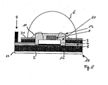
- FIG. 5 now shows the reverse case according to the invention, that is according to FIG. 5 the LED die 1 "face down” is arranged so that the substrate of the LEDs facing away from the metal core 5 of the board 17.
- the LED die 1 is arranged on an intermediate carrier 10 by means of a conductive adhesive 20.
- the conductive adhesive 20 has, for example, a thickness of less than 10 ⁇ m and a thermal conductivity of more than 2 W / mK.
- the electrical contact of the LED Dice 1 of FIG. 5 thus takes place via wires 11 which are contacted with the intermediate carrier 10.
- Such "face down” mounted LED dies usually have higher efficiencies compared to "face up” mounted LED dies.
- the intermediate carrier 10 is made of a ceramic material, for example, and has conductor tracks on its upper side, while the underside is optionally electrically insulated from the metal core 5 of the circuit board 17 by a further insulating layer 19. Again, however, the insulating layer 19 is so equipped that it is thermally well conductive.
- FIG. 6 a further embodiment according to the invention is shown, in which the LED Die 1 in turn “face down” is arranged on an intermediate carrier 10 in order to achieve the improved light output and thus higher brightness in this arrangement.
- This intermediate carrier is preferably an AlN (aluminum nitride) ceramic carrier substrate, which has excellent heat-conducting properties and at the same time has an electrically insulating effect.
- the advantage in the use of this additional intermediate carrier 10 is that a higher ESD (electrostatic discharge) strength is achieved and the metkallkernplatine remains electrically neutral.
- the LED 1 is now surrounded with a color conversion substance 13 in order to convert the light into a desired (mixed) color.
- the upper side of the electrically conductive layer 3 is further covered with an additional adhesive layer 21, the task of which is to fix the lens 6.
- an additional adhesive layer 21 the task of which is to fix the lens 6.
- a double-sided adhesive tape 22 is provided, which allows easy attachment of the entire light-emitting diode array.
Landscapes
- Led Device Packages (AREA)
- Cooling Or The Like Of Semiconductors Or Solid State Devices (AREA)
- Arrangement Of Elements, Cooling, Sealing, Or The Like Of Lighting Devices (AREA)
Description
Die vorliegende Erfindung bezieht sich auf Leuchtdioden-Anordnungen, bei denen LED-Dice (Leuchtdioden-Chips) auf einer wärmeabführenden Platine angeordnet sind.The present invention relates to light-emitting diode arrays in which LED dice (light-emitting diode chips) are arranged on a heat dissipating board.
Um Anwendungen mit LEDs mit hoher Helligkeit zu realisieren, werden in letzter Zeit immer mehr Hochleistungs-LEDs mit einer Betriebsleistung von mehr als 1 Watt (elektrisch) eingesetzt. Die Chipfläche dieser LED-Dice liegt derzeit im Bereich von 1mm2. Es ist zu erwarten, dass sich in der Zukunft die Betriebsleistung pro LED weiter erhöhen wird, was einerseits durch größere Halbleiter und andererseits durch höhere Stromdichten erreicht wird. Speziell die Erhöhung der Stromdichten bewirkt, dass die Leistungsdichten von LEDs in der nächsten Zeit von derzeit maximal 1 bis 2 Wattelektrisch/mm2 auf über 4 Wattelektrisch/mm2 ansteigen können.In order to realize applications with LEDs with high brightness, lately more and more high power LEDs with an operating power of more than 1 watt (electric) are used. The chip area of this LED dice is currently in the range of 1mm2. It is to be expected that in the future the operating power per LED will continue to increase, which is achieved on the one hand by larger semiconductors and on the other hand by higher current densities. In particular, increasing the current densities means that the power densities of LEDs can rise from the current maximum of 1 to 2 watts electrical / mm2 to more than 4 watts electrical / mm2 in the near future.
Bei Erhöhung der Leistungsdichten ist indessen gleichzeitig dafür zu sorgen, dass die entsprechend ebenfalls erhöhte Verlustwärme abgeführt wird, um sicherzustellen, dass die Verlustwärme ausreichend vom Halbleiter abgeführt wird.When increasing the power densities, however, care must be taken at the same time that the correspondingly increased heat loss is dissipated to ensure that the heat loss is dissipated sufficiently from the semiconductor.
Eine zu große Erwärmung der LEDs während des Betriebs führt nämlich u.U. zu einer Bauteilzerstörung. Aus diesem Grund muss während des Betriebs der LED gewährleistet sein, dass die Temperatur an der Sperrschicht des p-n Obergangs in der LED beilspielsweise 125°C nicht übersteigt. Diese Gefahr besteht genauer gesagt darin, dass nur ein Teil der von der LED aufgenommenen elektrischen Leistung in Leicht umgesetzt wird, während der andere Teil in Wärme umgewandelt wird (derzeit ist der Licht-Wirkungsgrad von LEDs noch unter 10%). Die Betriebsparameter von LEDs sind daher in Abhängigkeit von der Art der Montage (Assemblierung), der Einbau- und Umgebungsbedingungen derart zu wählen, dass die Sperrschichttemperatur der LED bspw. 125°C nicht übersteigt.Excessive heating of the LEDs during operation may lead to component destruction. For this reason, it must be ensured during operation of the LED that the temperature at the junction of the pn junction in the LED, for example, does not exceed 125 ° C. More specifically, this danger is that only part of the electrical power consumed by the LED is converted into light, while the other part is converted to heat (currently the light efficiency of LEDs is still below 10%). The operating parameters of LEDs, therefore, depending on the type of assembly (assembly), the installation and environmental conditions to be selected such that the junction temperature of the LED, for example. 125 ° C does not exceed.
Die Erfindung setzt dahingehend an, dass die Verlustwärme durch Verbesserung des thermischen Widerstands der Anordnung effizienter abgeführt werden kann. Wenn gemäß der Erfindung die Wärme gut durch geringen thermischen Widerstand abgeführt werden kann, kann diese ohne hohe Temperaturgefälle auf den LED-Träger übertragen werden. Der thermische Widerstand wird dabei in K(Kelvin) /W(Watt) ausgedrückt.The invention is to the effect that the heat loss can be dissipated by improving the thermal resistance of the device more efficient. If according to the invention, the heat can be dissipated well by low thermal resistance, it can be transferred without high temperature gradient on the LED carrier. The thermal resistance is expressed in K (Kelvin) / W (Watt).
Gemäß dem Stand der Technik sind Anordnungen für Hochleistungs-LEDs bekannt, die typischerweise einem thermischen Widerstand von mehr als 15 K/W in dem Bereich von der Sperrschicht zum LED-Träger (Platine oder dgl.) aufweisen. Dies bedeutet, dass gemäß dem Stand der Technik der Temperaturunterschied zwischen dem LED-Träger und der aktiven Zone (Sperrschicht) der LED bei einem Betrieb mit fünf Welektrisch bis zu 75 Kelvin betragen würde. Ausgehend von der genannten maximal zulässigen Sperrschichttemperatur in Dauerbetrieb bedeutet dies, dass bei einer Umgebungstemperatur von beilspielsweise 40°C der Temperaturabfall über einen Wärmetauscher (Kühlkörper) maximal 10°C betragen darf. Dies würde wiederum eine Kühloberfläche von 350 cm2 erfordern, was ganz offensichtlich Probleme mit sich bringt. Darüber hinaus wäre ein Einsatz bei Temperaturen über 50°C nahezu unmöglich, was die Verwendung der LED für bestimmte technische Anwendungen, wie beispielsweise im Kfz-Bereich unmöglich machen würde.In the prior art arrangements for high power LEDs are known, which typically have a thermal resistance of more than 15 K / W in the area from the barrier to the LED carrier (board or the like). This means that according to the prior art, the temperature difference between the LED substrate and the active zone (barrier layer) would be of the LED during operation with five W electrically up to 75 Kelvin. Based on the maximum permitted junction temperature in continuous operation, this means that at an ambient temperature of about 40 ° C, the temperature drop across a heat exchanger (heat sink) may not exceed 10 ° C. This in turn would require a cooling surface of 350
Aus dem Stand der Technik ist es bekannt, als LED-Träger gedruckte Leiterplatten (printed circuit boards, PCBs) zu verwenden. Üblicherweise weisen diese ein organisches Epoxidharz auf, das thermisch nur sehr schlecht leitet und daher die thermische Ableitung der Verlustwärme von der LED auf den Träger erschwert.It is known from the prior art to use printed circuit boards (PCBs) as LED carriers. Usually, these have an organic epoxy resin, which conducts very poorly thermally and therefore impedes the thermal dissipation of the heat loss from the LED to the carrier.
Alternativ sind auch Keramikplatinen bekannt, die zwar bessere thermische Eigenschaften im Vergleich zu den Leiterplatten auf Epoxidharzbasis aufweisen, dagegen aber sehr spröde und brüchig sind, was ihre Verwendung als Trägermaterial mehr als einschränkt.Alternatively, ceramic boards are known, which, although better thermal properties compared to the printed circuit boards based on epoxy resin, but are very brittle and fragile, which more than limits their use as a carrier material.
In technischen Hochleistungsanwendungen werden gemäß dem Stand der Technik auch Metallkernplatinen eingesetzt. Diese haben typischerweise einen sandwichartigen Aufbau basierend aus der Metallkernbasis, einer Isolationsschicht und einer Leiterbahn.In high-performance technical applications, metal core boards are also used in the prior art. These typically have a sandwich-type structure based on the metal core base, an insulation layer and a conductor track.
Angesichts dieses Standes der Technik ist es Aufgabe der vorliegenden Erfindung, eine Montage-Anordnung für Leuchtdioden mit verbesserter Wärmeabfuhr vorzuschlagen.In view of this prior art, it is an object of the present invention to propose a mounting arrangement for light-emitting diodes with improved heat dissipation.
Die Erfindung geht dabei von der Erkenntnis aus, dass nach Stand der Technik bei der Verwendung von Metallkernplatinen die Abfuhr der Verlustwärme von der LED, welche auf die Leiterbahn aufgesetzt ist, durch die darunterliegende Isolationsschicht eingeschränkt ist, was wiederum die Leistungsdichte der LED eingrenzt.The invention is based on the recognition that the prior art in the use of metal core boards, the dissipation of heat loss from the LED, which is placed on the conductor, is limited by the underlying insulating layer, which in turn limits the power density of the LED.
Die angeführte Aufgabe wird erfindungsgemäß durch die Merkmale der unabhängigen Ansprüche gelöst. Die abhängigen Ansprüche bilden den zentralen Gedanken der Erfindung in besonders vorteilhafter Weise weiter.The stated object is achieved by the features of the independent claims. The dependent claims further form the central idea of the invention in a particularly advantageous manner.
Gemäß der Erfindung ist also eine Leuchtdioden-Anordnung mit wenigstens einem Leuchtdioden-Chip (LED-Die) vorgesehen. Weiterhin ist eine Mehrschichtplatine aufweisend eine Basis aus einem thermisch gut leitfähigen Material, wie beispielsweise Metall vorgesehen, wobei die Basis ein Kern der Platine ist und zur Wärmeabfuhr dient und wobei eine elektrisch isolierende und thermisch leitende Verbindungsschicht zwischen der Emissionsfläche des Leuchtdioden-Chips und der Platine angeordnet ist. Der Leuchtdioden-Chip ist derart angeordnet" dass das Substrat der Leuchtdioden von der Platine abgewandt ist, wobei zwischen dem Leuchtdioden-Chip und der Basis der Platine ein zu diesen Teilen separater Zwischenträger angeordnet ist, mit dem der Leuchtdioden-Chip elektrisch kontaktiert ist, wobei der Zwischenträger durch ein Aluminiumnitrid-Substrat gebildet ist, wobei die elektrisch isolierende Verbindungsschicht eine Klebefolie ist, welche direkt auf der Basis angeordnet ist und auf welcher direkt der Zwischenträger angeordnet ist. Da im Gegensatz zum Stand der Technik die thermisch isolierende (Epoxid-) Schicht in Wegfall gelangt, wird der Wärmeübertrag von dem Leuchtdioden-Chip zu dem wärmeabführenden Basismaterial der Platine hin deutlich verbessert.According to the invention, therefore, a light-emitting diode arrangement with at least one light-emitting diode chip (LED die) is provided. Furthermore, a multilayer board comprising a base of a thermally highly conductive material, such as metal is provided, the base is a core of the board and is used for heat dissipation and wherein an electrically insulating and thermally conductive bonding layer between the emitting surface of the LED chip and the board is arranged. The light-emitting diode chip is arranged such that the substrate of the light-emitting diodes faces away from the printed circuit board, wherein an intermediate carrier separate from these parts is arranged between the light-emitting diode chip and the base of the printed circuit board, with which the light-emitting diode chip is electrically contacted the intermediate carrier is formed by an aluminum nitride substrate, wherein the electrically insulating connecting layer is an adhesive film, which is arranged directly on the base and on which the intermediate carrier is arranged directly Contrary to the prior art, the thermal insulating (epoxy) layer is eliminated, the heat transfer from the LED chip to the heat dissipating base material of the board is significantly improved.
Eine isolierende Klebeschicht, die durch eine Klebefolie realisiert ist, ist insbesondere dann von Vorteil, wenn ein Leuchtdioden-Chip verwendet wird, dessen der Basis zugewandte Oberfläche elektrisch leitend ist. In diesem Fall muss eine gesonderte elektrische Isolierung zwischen dem Chip und der Basis erfolgen, um Kurzschlüsse und ESD-Ausfälle zu vermeiden.An insulating adhesive layer, which is realized by an adhesive film, is particularly advantageous if a light-emitting diode chip is used, whose base-facing surface is electrically conductive. In this case, separate electrical isolation must be provided between the chip and the base to prevent short circuits and ESD failures.
Der Leuchtdioden-Chip kann in einer Vertiefung der Platine untergebracht sein. Dabei kann der Leuchtdioden-Chip derart versenkt sein, dass seine Oberseite nicht über die Kontur der Platine übersteht und beispielsweise plan mit der Oberseite der Platine abschließt.The light-emitting diode chip can be accommodated in a recess of the board. In this case, the light-emitting diode chip can be sunk in such a way that its upper side does not protrude beyond the contour of the board and, for example, terminates flush with the upper side of the board.
Die Vertiefung, in die der LED-Chip gesetzt ist, kann dabei in der wärmeabführenden Basis der Platine ausgebildet sein.The recess into which the LED chip is set, can be formed in the heat-dissipating base of the board.
Gleichzeitig kann die Vertiefung weitere Funktionen aufweisen. Beispielsweise kann die Vertiefung eine Reflektorwirkung haben, wobei vorteilhafterweise die Wände der Vertiefung zumindest teilweise abgeschrägt sind.At the same time, the depression can have further functions. For example, the recess may have a reflector effect, wherein advantageously the walls of the recess are at least partially bevelled.
Insbesondere ist die Leuchtdioden-Anordnung durch die "Face Down"-Montagetechnik gebildet, bei der der Leuchtdioden-Chip derart angeordnet ist, dass das Substrat der Leuchtdioden von der Platine abgewandt ist.In particular, the light-emitting diode arrangement is formed by the "face-down" mounting technique, in which the light-emitting diode chip is arranged such that the substrate of the light-emitting diodes faces away from the circuit board.
Der Leuchtdioden-Chip kann mittels eines Leitklebers auf dem Zwischenträger angeordnet sein.The light-emitting diode chip can be arranged on the intermediate carrier by means of a conductive adhesive.
Die der Platine zugewandte Seite des Zwischenträgers kann elektrisch isolierend sein, wobei der dem Leuchtdioden-Chip zugewandte Bereich des Zwischenträgers leitende Bereiche wie beispielsweise Leiterbahnen aufweisen kann.The side of the intermediate carrier facing the printed circuit board can be electrically insulating, wherein the region of the intermediate carrier facing the light-emitting diode chip can have conductive regions, such as conductor tracks.
Wenigstens der Bereich des wenigstens einen Leuchtdioden-Chips kann von einer Linse wie beispielsweise einer Fresnel-Linse überdeckt sein.At least the region of the at least one light-emitting diode chip may be covered by a lens, such as a Fresnel lens.
Der Bereich zwischen der Platine und der Linse kann wenigstens teilweise mit einem Farbkonversionsstoff gefüllt sein. Der Farbkonversionsstoff kann also neben und/oder über dem Leuchtdioden-Chip angeordnet sein. Gegebenenfalls kann auch die Vertiefung seitlich vom Chip mit einem Farbkonversionsstoff aufgefüllt sein, um eine LED mit wesentlich weißer Lichtcharakteristik zu erhalten.The area between the board and the lens may be at least partially filled with a color conversion substance. The color conversion substance can therefore be arranged next to and / or above the light-emitting diode chip. Optionally, also the recess can be filled laterally from the chip with a color conversion substance to obtain an LED with a substantially white light characteristic.
Der Leuchtdioden-Chip kann mittels Drähten von einer Leiterplatte aus kontaktiert sein, wobei diese Leiterplatte seitlich von dem Leuchtdioden-Chip sandwichartig mittels einer dazwischenliegenden Isolierschicht auf der Platine aufgebracht ist.The light-emitting diode chip can be contacted by means of wires from a printed circuit board, wherein this printed circuit board is laterally applied by the light-emitting diode chip sandwiched by means of an intermediate insulating layer on the board.
Weitere Merkmale, Vorteile und Eigenschaften der vorliegenden Erfindung sollen nunmehr unter Bezugnahme auf die Figuren der begleitenden Zeichnungen erläutert werden.
-
Figur 1 -
Figur 2Figur 1 -
Figur 3Figur 2 -
Figur 4 -
Figur 5 -
Figur 6
-
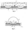
FIG. 1 shows an example of an LED arrangement, -
FIG. 2 shows a modification ofFIG. 1 in that in the metal base material a depression is provided in which the LED die is inserted, -
FIG. 3 shows a modification ofFIG. 2 in that the recess of the carrier is filled in total with a color conversion substance, -
FIG. 4 shows how a multi-LED dice LED array can be covered by a flat Fresnel lens, -
FIG. 5 shows an embodiment of the invention, in which the LED is the "Face Down" mounted, and -
FIG. 6 shows a further embodiment of the invention, in which the LED is the "Face Down" mounted.
Wie oben bereits ausgeführt, soll gemäß der vorliegenden Erfindung ein LED-Die möglichst direkt auf die wärmeableitende Basis beispielsweise einer Metallkernplatine aufgesetzt sein. Bei diesem Schritt muss indessen das Problem überwunden werden, dass LED-Dies häufig über das LED-Substrat bzw. über ihre der Basis zugewandte Oberfläche leitfähig sind, wodurch sich bei einer derartigen Anordnung ein Kurzschluss zum Leiterplattenbasismaterial ergeben kann, der oft unerwünscht ist und besonders hinsichtlich der Verschaltungsmöglichkeiten der LEDs keinerlei Designfreiheit lässt.As already stated above, according to the present invention, an LED should be placed as directly as possible on the heat dissipating base, for example, a metal core board. However, this step must overcome the problem that LED dies are often conductive across the LED substrate or its base-facing surface, which can result in a short circuit to the printed circuit board base material, which is often undesirable and particularly so regarding the wiring options of the LEDs no design freedom.
Wie aus dem Beispiel der
Die Metallkernplatine 17 weist neben diesem Basis-Metallkern 5 eine darüberliegende elektrisch isolierende Schicht 4 sowie eine elektrisch leitfähige Schicht mit Leiterbahnen 3 auf, wobei vorzugsweise die elektrisch isolierende Schicht 4 und die Leiterbahnen-Schicht 3 deckungsgleiche Ausnehmungen 16 aufweisen, in die der LED-Die 1 eingesetzt ist.The
Die elektrische Kontaktierung des LED-Dies erfolgt bei dieser Anordnung, bei der das Substrat des LED-Dies der Platine 1) zugewandt ist, seitlich von den Leiterbahnen 3 mittels Drähten 11 auf die Oberseite des LED-Dice 1.The electrical contacting of the LED dies occurs in this arrangement, in which the substrate of the LED dies facing the printed circuit board 1), laterally from the printed
Auf der Unterseite des Basismaterials 5 der Metallkernplatine 7 können weitere Kühlkörper 14 bekannter Art angeordnet sein.On the underside of the
Insbesondere der Bereich des LED-Dies 1 und der Ausnehmung 16 kann von einer im Wesentlichen kalottenförmigen Linse 6 überdeckt sein, die das vom dem LED-Die 1 abgestrahlte Licht bündelt.In particular, the region of the LED dies 1 and the
Die elektrische Kontaktierung der in
Als Basismaterial 5 der Platine 17 wird allgemein ein Material mit hoher thermischer Leitfähigkeit eingesetzt, so dass bevorzugt Metalle, wie beispielsweise Aluminium oder Kupfer zur Verwendung kommen können.As the
Die elektrisch isolierende aber thermisch leitfähige Verbindungsschicht 2 kann zum Beispiel eine nicht leitende Substratschicht der LEDs (für grüne LEDs wird z. B. oftmals Saphir verwendet) oder aber auch ein thermisch leitfähiger und elektrisch isolierender Kleber sein. Die elektrisch isolierende aber thermisch leitfähige Verbindungsschicht 2 kann also Teil des LED-Dies 1, der Mehrschichtplatine 17 und/oder eine davon separate Schicht sein. Die separate Schicht ist insbesondere dann erforderlich, wenn die LED-Dies 1 derart angeordnet sind, dass ihre der Mehrschichtplatine 17 zugewandte Oberfläche elektrisch leitfähig ist. Ferner ist beispielsweise bei roten LEDs, die aus zwei übereinander angeordneten Dioden-Schichten bestehen, immer eine der beiden Schichten der Mehrschichtplatine 17 zugewandt, weshalb zur Vermeidung von Kurzschlüssen und ESD-Ausfällen eine separate Isolierung erforderlich ist.The electrically insulating but thermally
Die Isolationsschicht 4 der Metallkernplatine 17 kann beispielsweise aus organischen Materialien oder dünnen Keramiken bestehen (letztere sind z. B. auf den Metallträger 5 aufgeschlämmt, bzw. der Metallträger wird mit einem eingebrannten Keramiktape beschichtet.The insulating
In dem Beispiel von
Somit dient das Basismaterial 5 der Mehrschichtplatine 17 nicht nur zur Befestigung und Wärmeabfuhr des LED-Dies 1, sondern auch zur gezielten Lichtlenkung in Richtung weg von der Platine. Diese Lichtlenkung durch die Reflektorwirkung der Vertiefung 18 im Basismaterial 5 der Platine 17 ist vorzugsweise mit der Wirkung der Linse 6 abgestimmt.Thus, the
Es ist aus dem Stand der Technik bekannt, dass mittels Farbkonversionsmitteln "weiße LEDs" erreicht werden können. Derartige LEDs werden in der Fachwelt oft auch als "Phosphorkonverter-LEDs" oder "Lumineszenzkonversions-LEDs" bezeichnet. Wie aus
Bei dem Beispiel von
Die Beispiele von
Der Zwischenträger 10 ist beispielsweise aus einem Keramikmaterial und weist auf seiner Oberseite Leiterbahnen auf, während die Unterseite gegebenenfalls durch eine weitere Isolationsschicht 19 gegenüber dem Metallkern 5 der Platine 17 elektrisch isoliert ist. Wiederum ist indessen auch die Isolierschicht 19 so ausgestattet, dass sie thermisch gut leitfähig ist.The
Abschließend ist in
Ergänzend zu der Ausführungsform in
Claims (14)
- Light-emitting diode arrangement, comprising:- at least one light-emitting diode chip (1),- a multilayered plate (17) having a base (5) consisting of a material with good thermal conductivity, in particular of metal, wherein the base (5) is a core of the plate (17) and is used for heat dissipation, and- an electrically insulating and thermally conductive connecting layer (2) between the emission area of the light-emitting diode chip (1) and the plate,
wherein the light-emitting diode chip (1) is arranged in such a way that the substrate of the light-emitting diodes faces away from the plate (17),
wherein arranged between the light-emitting diode chip (1) and the base (5) of the plate (17) is an intermediate carrier (10) which is separate from said parts and is used to make electrical contact with the light-emitting diode chip (1),
characterized in that
the intermediate carrier (10) is formed by an aluminium nitride substrate, and
the electrically insulating connecting layer (2) is an adhesive film, which is arranged directly on the base (5) and on which the intermediate carrier (10) is arranged directly. - Arrangement according to one of the preceding claims, characterized in that the light-emitting diode chip (1) is accommodated in a depression (16) in the plate (17).
- Arrangement according to one of the preceding claims, characterized in that the light-emitting diode chip (1) is arranged in the region of a depression (12) in the base material (5) of the plate (17).
- Arrangement according to Claim 2 or 3, characterized in that the light-emitting diode chip (1) does not protrude beyond the contour of the plate (5).
- Arrangement according to one of Claims 2 to 4, characterized in that the light-emitting diode chip (1) terminates level with the upper side of the plate (17).
- Arrangement according to one of Claims 2 to 4, characterized in that the depression (12, 16) has the function of a reflector.
- Arrangement according to one of Claims 2 to 6, characterized in that the walls of the depression (12, 16) are at least partially bevelled.
- Arrangement according to one of the preceding claims, characterized in that the light-emitting diode chip (1) is arranged on the intermediate carrier (10) by means of a conductive adhesive (20).
- Arrangement according to one of the preceding claims, characterized in that that side of the intermediate carrier (10) which faces the plate (17) is electrically insulating.
- Arrangement according to Claim 9, characterized in that that region of the intermediate carrier (10) which faces the light-emitting diode chip (1) has conductive regions.
- Arrangement according to one of the preceding claims, characterized in that at least the region of the light-emitting diode chip (1) is covered by a lens (6), in particular a Fresnel lens (9).
- Arrangement according to Claim 11, characterized in that that region between the plate (17) and the lens (6, 9) is filled at least partially with a colour conversion material (13).
- Arrangement according to Claim 12, characterized in that the colour conversion material (13) is arranged over and next to the light-emitting diode chip (1).
- Arrangement according to one of the preceding claims, characterized in that contact is made with the light-emitting diode chip (1) by means of wires (11) from a printed circuit board (3), which is fitted on the plate (17) in the manner of a sandwich by means of an interposed insulating layer (4).
Applications Claiming Priority (2)
| Application Number | Priority Date | Filing Date | Title |
|---|---|---|---|
| DE10351934.3A DE10351934B4 (en) | 2003-11-07 | 2003-11-07 | Light-emitting diode arrangement with heat dissipating board |
| PCT/EP2004/012438 WO2005048358A1 (en) | 2003-11-07 | 2004-11-03 | Light-emitting diode arrangement comprising a heat-dissipating plate |
Publications (2)
| Publication Number | Publication Date |
|---|---|
| EP1680818A1 EP1680818A1 (en) | 2006-07-19 |
| EP1680818B1 true EP1680818B1 (en) | 2014-05-21 |
Family
ID=34559429
Family Applications (1)
| Application Number | Title | Priority Date | Filing Date |
|---|---|---|---|
| EP04818383.4A Expired - Lifetime EP1680818B1 (en) | 2003-11-07 | 2004-11-03 | Light-emitting diode arrangement comprising a heat-dissipating plate |
Country Status (8)
| Country | Link |
|---|---|
| US (1) | US8766283B2 (en) |
| EP (1) | EP1680818B1 (en) |
| JP (1) | JP2007510297A (en) |
| KR (1) | KR101116723B1 (en) |
| CN (1) | CN100442552C (en) |
| AU (1) | AU2004310132B2 (en) |
| DE (1) | DE10351934B4 (en) |
| WO (1) | WO2005048358A1 (en) |
Families Citing this family (36)
| Publication number | Priority date | Publication date | Assignee | Title |
|---|---|---|---|---|
| DE102005049858B3 (en) * | 2005-10-18 | 2007-02-01 | Benq Mobile Gmbh & Co. Ohg | Multilayer circuit-board for communication terminals, has one or more transparent layers joined to one or more decoupling points |
| JP5066333B2 (en) * | 2005-11-02 | 2012-11-07 | シチズン電子株式会社 | LED light emitting device. |
| JP2007208061A (en) * | 2006-02-02 | 2007-08-16 | Sharp Corp | Semiconductor light emitting element, manufacturing method thereof, and assembly thereof |
| JP2007234886A (en) * | 2006-03-01 | 2007-09-13 | Compal Communications Inc | Electronic element assembly with thermal dissipation constitution |
| TWI314366B (en) * | 2006-04-28 | 2009-09-01 | Delta Electronics Inc | Light emitting apparatus |
| TWI306674B (en) * | 2006-04-28 | 2009-02-21 | Delta Electronics Inc | Light emitting apparatus |
| CN101079460B (en) * | 2006-05-23 | 2010-05-12 | 台达电子工业股份有限公司 | Lighting device |
| DE102006043882A1 (en) | 2006-09-19 | 2008-03-27 | Giesecke & Devrient Gmbh | Sensor for analyzing a document of value and method for producing the sensor |
| DE102006059702A1 (en) * | 2006-09-29 | 2008-04-03 | Osram Opto Semiconductors Gmbh | Opto-electronic element has metal core plate, metal core, dielectric layer applied on metal core and electrically conductive layer applied on dielectric layer and element also has chip carrier connected with metal core plate |
| KR20080057881A (en) * | 2006-12-21 | 2008-06-25 | 엘지전자 주식회사 | Printed circuit board, light emitting apparatus having the same and method for manufacturing thereof |
| DE102008021618A1 (en) * | 2007-11-28 | 2009-06-04 | Osram Opto Semiconductors Gmbh | Chip arrangement, connection arrangement, LED and method for producing a chip arrangement |
| CN101546754A (en) * | 2008-03-26 | 2009-09-30 | 富准精密工业(深圳)有限公司 | LED module |
| JP2009239036A (en) * | 2008-03-27 | 2009-10-15 | Hitachi Aic Inc | Led substrate |
| US20100078661A1 (en) * | 2008-09-26 | 2010-04-01 | Wei Shi | Machined surface led assembly |
| US9252336B2 (en) | 2008-09-26 | 2016-02-02 | Bridgelux, Inc. | Multi-cup LED assembly |
| TW201017922A (en) * | 2008-10-23 | 2010-05-01 | Everlight Electronics Co Ltd | Light emitting diode package |
| KR101064793B1 (en) * | 2009-06-08 | 2011-09-14 | 박종진 | Radiant heat led board |
| JP2011066028A (en) * | 2009-09-15 | 2011-03-31 | Hitachi Ltd | Multi-wavelength light source device |
| WO2011034259A1 (en) * | 2009-09-17 | 2011-03-24 | 포인트엔지니어링 | Optical element substrate, optical element device, and method for manufacturing same |
| DE102009060781A1 (en) * | 2009-12-22 | 2011-06-30 | Automotive Lighting Reutlingen GmbH, 72762 | Light module for a lighting device of a motor vehicle and lighting device with such a light module |
| DE102011003608A1 (en) * | 2010-08-20 | 2012-02-23 | Tridonic Gmbh & Co. Kg | Housed LED module |
| CN102052594A (en) * | 2010-12-20 | 2011-05-11 | 惠州志能达光电科技有限公司 | LED (light emitting diode) light source module with high heat dissipation and manufacturing method thereof |
| TWI464929B (en) * | 2011-03-16 | 2014-12-11 | Lextar Electronics Corp | Light source module with enhanced heat dissipation efficiency and embedded package structure thereof |
| US8603858B2 (en) * | 2011-07-12 | 2013-12-10 | Infineon Technologies Ag | Method for manufacturing a semiconductor package |
| KR101321001B1 (en) * | 2011-12-26 | 2013-10-22 | 주식회사 루멘스 | Light emitting diode package, and method for manufacturing the light emitting device package |
| JP2013201256A (en) * | 2012-03-23 | 2013-10-03 | Toshiba Lighting & Technology Corp | Wiring board device, light-emitting module, lighting device, and method for manufacturing wiring board device |
| FI125565B (en) * | 2012-09-08 | 2015-11-30 | Lumichip Ltd | LED chip-on-board component and lighting module |
| KR101974348B1 (en) * | 2012-09-12 | 2019-05-02 | 삼성전자주식회사 | Light emitting device package and method of manufacturing the same |
| US8927398B2 (en) * | 2013-01-04 | 2015-01-06 | International Business Machines Corporation | Group III nitrides on nanopatterned substrates |
| CN103152976B (en) * | 2013-03-25 | 2016-06-15 | 乐健科技(珠海)有限公司 | For the ceramic base printed circuit board that LED installs |
| KR101431588B1 (en) | 2013-04-09 | 2014-08-29 | 주식회사 굿엘이디 | Chip on board Light-Emitting Diode package of high efficiency |
| CN104009028B (en) * | 2014-05-26 | 2017-06-06 | 上海信耀电子有限公司 | The high power LED integration packaging method and structure of ceramic substrate and heat radiation substrate |
| CN108091705B (en) * | 2014-05-27 | 2019-07-02 | 太阳能公司 | Stacking formula solar cell module |
| US11949026B2 (en) | 2014-05-27 | 2024-04-02 | Maxeon Solar Pte. Ltd. | Shingled solar cell module |
| CN106206905B (en) * | 2015-04-29 | 2019-01-15 | 光宝光电(常州)有限公司 | Light-emitting diode encapsulation structure |
| CN105805694A (en) * | 2016-04-07 | 2016-07-27 | 深圳市华星光电技术有限公司 | Quantum dot light source and quantum dot backlight module |
Family Cites Families (29)
| Publication number | Priority date | Publication date | Assignee | Title |
|---|---|---|---|---|
| US4713579A (en) * | 1984-11-12 | 1987-12-15 | Takiron Co., Ltd. | Dot matrix luminous display |
| JPH0680841B2 (en) * | 1986-04-07 | 1994-10-12 | 株式会社小糸製作所 | Lighting equipment |
| US5529852A (en) * | 1987-01-26 | 1996-06-25 | Sumitomo Electric Industries, Ltd. | Aluminum nitride sintered body having a metallized coating layer on its surface |
| KR880014692A (en) * | 1987-05-30 | 1988-12-24 | 강진구 | Semiconductor Light Emitting Device with Reflector |
| JPH01313969A (en) * | 1988-06-13 | 1989-12-19 | Hitachi Ltd | Semiconductor device |
| US5512131A (en) * | 1993-10-04 | 1996-04-30 | President And Fellows Of Harvard College | Formation of microstamped patterns on surfaces and derivative articles |
| JP3165779B2 (en) * | 1995-07-18 | 2001-05-14 | 株式会社トクヤマ | Submount |
| US6608332B2 (en) * | 1996-07-29 | 2003-08-19 | Nichia Kagaku Kogyo Kabushiki Kaisha | Light emitting device and display |
| US6441943B1 (en) * | 1997-04-02 | 2002-08-27 | Gentex Corporation | Indicators and illuminators using a semiconductor radiation emitter package |
| JPH11112028A (en) * | 1997-10-02 | 1999-04-23 | Matsushita Electron Corp | Semiconductor light emitting device |
| DE29804489U1 (en) * | 1998-03-13 | 1998-05-20 | Reitter & Schefenacker GmbH & Co. KG, 73730 Esslingen | Exterior rear view mirror for vehicles, preferably for motor vehicles |
| US6335548B1 (en) * | 1999-03-15 | 2002-01-01 | Gentex Corporation | Semiconductor radiation emitter package |
| EP1056971A1 (en) * | 1998-12-17 | 2000-12-06 | Koninklijke Philips Electronics N.V. | Light engine |
| CN1135638C (en) * | 1999-10-14 | 2004-01-21 | 凌士忠 | LED unit |
| TW465123B (en) | 2000-02-02 | 2001-11-21 | Ind Tech Res Inst | High power white light LED |
| US6428189B1 (en) * | 2000-03-31 | 2002-08-06 | Relume Corporation | L.E.D. thermal management |
| JP4432275B2 (en) | 2000-07-13 | 2010-03-17 | パナソニック電工株式会社 | Light source device |
| JP2002042525A (en) * | 2000-07-26 | 2002-02-08 | Toyoda Gosei Co Ltd | Planar light source |
| US6874910B2 (en) * | 2001-04-12 | 2005-04-05 | Matsushita Electric Works, Ltd. | Light source device using LED, and method of producing same |
| JP2002319705A (en) * | 2001-04-23 | 2002-10-31 | Matsushita Electric Works Ltd | Led device |
| US20040012958A1 (en) * | 2001-04-23 | 2004-01-22 | Takuma Hashimoto | Light emitting device comprising led chip |
| JP2003008069A (en) | 2001-06-19 | 2003-01-10 | Sanyo Electric Co Ltd | Light emitting device |
| JP4045781B2 (en) * | 2001-08-28 | 2008-02-13 | 松下電工株式会社 | Light emitting device |
| US20050073846A1 (en) * | 2001-09-27 | 2005-04-07 | Kenji Takine | Lightemitting device and method of manufacturing the same |
| US6498355B1 (en) | 2001-10-09 | 2002-12-24 | Lumileds Lighting, U.S., Llc | High flux LED array |
| JP4269709B2 (en) * | 2002-02-19 | 2009-05-27 | 日亜化学工業株式会社 | Light emitting device and manufacturing method thereof |
| US6924514B2 (en) * | 2002-02-19 | 2005-08-02 | Nichia Corporation | Light-emitting device and process for producing thereof |
| US6682331B1 (en) * | 2002-09-20 | 2004-01-27 | Agilent Technologies, Inc. | Molding apparatus for molding light emitting diode lamps |
| DE20300626U1 (en) * | 2002-11-19 | 2003-05-28 | electronic service willms GmbH & Co. KG, 52223 Stolberg | Chip card for Light Emitting Diode has heat bridges between top mounting surface and cooling baseplate and has central mounting for Light Emitting Diode |
-
2003
- 2003-11-07 DE DE10351934.3A patent/DE10351934B4/en not_active Expired - Lifetime
-
2004
- 2004-11-03 AU AU2004310132A patent/AU2004310132B2/en not_active Ceased
- 2004-11-03 US US10/578,362 patent/US8766283B2/en not_active Expired - Fee Related
- 2004-11-03 KR KR1020067008768A patent/KR101116723B1/en not_active IP Right Cessation
- 2004-11-03 WO PCT/EP2004/012438 patent/WO2005048358A1/en active Application Filing
- 2004-11-03 CN CNB2004800322635A patent/CN100442552C/en not_active Expired - Fee Related
- 2004-11-03 JP JP2006537246A patent/JP2007510297A/en active Pending
- 2004-11-03 EP EP04818383.4A patent/EP1680818B1/en not_active Expired - Lifetime
Also Published As
| Publication number | Publication date |
|---|---|
| KR20060115740A (en) | 2006-11-09 |
| WO2005048358A1 (en) | 2005-05-26 |
| KR101116723B1 (en) | 2012-03-08 |
| AU2004310132B2 (en) | 2010-04-22 |
| CN100442552C (en) | 2008-12-10 |
| US20070138488A1 (en) | 2007-06-21 |
| US8766283B2 (en) | 2014-07-01 |
| AU2004310132A1 (en) | 2005-05-26 |
| JP2007510297A (en) | 2007-04-19 |
| DE10351934B4 (en) | 2017-07-13 |
| EP1680818A1 (en) | 2006-07-19 |
| CN1875493A (en) | 2006-12-06 |
| DE10351934A1 (en) | 2005-06-09 |
Similar Documents
| Publication | Publication Date | Title |
|---|---|---|
| EP1680818B1 (en) | Light-emitting diode arrangement comprising a heat-dissipating plate | |
| EP2397754B1 (en) | Carrier body for construction elements or circuits | |
| DE102004044149B4 (en) | High-performance light emitting diode device | |
| EP1547163B1 (en) | Optoelectronic component | |
| EP3008753B1 (en) | Power module | |
| EP2143139B1 (en) | Cooling box for components or circuits | |
| EP3542399A1 (en) | Power module that is less prone to faults, and use thereof | |
| WO2017182159A1 (en) | Multi-layer carrier system, method for producing a multi-layer carrier system and use of a multi-layer carrier system | |
| DE102016115692A1 (en) | Thermally efficient electrical arrangement | |
| DE102017118490A1 (en) | LED module | |
| DE102012101560B4 (en) | light emitting diode device | |
| EP2398080B1 (en) | Light emitting diode based light source | |
| DE60037650T2 (en) | MULTICHIP MODULE FOR HIGH PERFORMANCE APPLICATIONS | |
| EP2580946A2 (en) | Light-emitting diode arrangement and light-emitting means, in particular with such a light-emitting diode arrangement | |
| WO2017182157A1 (en) | Carrier system | |
| DE102004035746B4 (en) | The power semiconductor module | |
| DE20307468U1 (en) | Light emitting diode circuit on three-layer board, includes through-contacts for thermal dissipation at diode contact areas |
Legal Events
| Date | Code | Title | Description |
|---|---|---|---|
| PUAI | Public reference made under article 153(3) epc to a published international application that has entered the european phase |
Free format text: ORIGINAL CODE: 0009012 |
|
| 17P | Request for examination filed |
Effective date: 20060330 |
|
| AK | Designated contracting states |
Kind code of ref document: A1 Designated state(s): AT BE BG CH CY CZ DE DK EE ES FI FR GB GR HU IE IS IT LI LU MC NL PL PT RO SE SI SK TR |
|
| RIN1 | Information on inventor provided before grant (corrected) |
Inventor name: TASCH, STEFAN Inventor name: HOSCHOPF, HANS |
|
| DAX | Request for extension of the european patent (deleted) | ||
| RAP1 | Party data changed (applicant data changed or rights of an application transferred) |
Owner name: TRIDONICATCO OPTOELECTRONICS GMBH |
|
| RAP1 | Party data changed (applicant data changed or rights of an application transferred) |
Owner name: LEDON LIGHTING JENNERSDORF GMBH |
|
| 17Q | First examination report despatched |
Effective date: 20090807 |
|
| RAP1 | Party data changed (applicant data changed or rights of an application transferred) |
Owner name: TRIDONIC JENNERSDORF GMBH |
|
| REG | Reference to a national code |
Ref country code: DE Ref legal event code: R079 Ref document number: 502004014624 Country of ref document: DE Free format text: PREVIOUS MAIN CLASS: H01L0033000000 Ipc: H01L0033640000 |
|
| GRAP | Despatch of communication of intention to grant a patent |
Free format text: ORIGINAL CODE: EPIDOSNIGR1 |
|
| RIC1 | Information provided on ipc code assigned before grant |
Ipc: H05K 1/18 20060101ALI20131126BHEP Ipc: H05K 1/02 20060101ALI20131126BHEP Ipc: H01L 33/64 20100101AFI20131126BHEP |
|
| INTG | Intention to grant announced |
Effective date: 20131212 |
|
| GRAS | Grant fee paid |
Free format text: ORIGINAL CODE: EPIDOSNIGR3 |
|
| GRAA | (expected) grant |
Free format text: ORIGINAL CODE: 0009210 |
|
| AK | Designated contracting states |
Kind code of ref document: B1 Designated state(s): AT BE BG CH CY CZ DE DK EE ES FI FR GB GR HU IE IS IT LI LU MC NL PL PT RO SE SI SK TR |
|
| REG | Reference to a national code |
Ref country code: GB Ref legal event code: FG4D Free format text: NOT ENGLISH |
|
| REG | Reference to a national code |
Ref country code: CH Ref legal event code: EP |
|
| REG | Reference to a national code |
Ref country code: AT Ref legal event code: REF Ref document number: 669989 Country of ref document: AT Kind code of ref document: T Effective date: 20140615 |
|
| REG | Reference to a national code |
Ref country code: IE Ref legal event code: FG4D Free format text: LANGUAGE OF EP DOCUMENT: GERMAN |
|
| REG | Reference to a national code |
Ref country code: DE Ref legal event code: R096 Ref document number: 502004014624 Country of ref document: DE Effective date: 20140703 |
|
| REG | Reference to a national code |
Ref country code: NL Ref legal event code: VDEP Effective date: 20140521 |
|
| PG25 | Lapsed in a contracting state [announced via postgrant information from national office to epo] |
Ref country code: IS Free format text: LAPSE BECAUSE OF FAILURE TO SUBMIT A TRANSLATION OF THE DESCRIPTION OR TO PAY THE FEE WITHIN THE PRESCRIBED TIME-LIMIT Effective date: 20140921 Ref country code: GR Free format text: LAPSE BECAUSE OF FAILURE TO SUBMIT A TRANSLATION OF THE DESCRIPTION OR TO PAY THE FEE WITHIN THE PRESCRIBED TIME-LIMIT Effective date: 20140822 Ref country code: FI Free format text: LAPSE BECAUSE OF FAILURE TO SUBMIT A TRANSLATION OF THE DESCRIPTION OR TO PAY THE FEE WITHIN THE PRESCRIBED TIME-LIMIT Effective date: 20140521 |
|
| PG25 | Lapsed in a contracting state [announced via postgrant information from national office to epo] |
Ref country code: ES Free format text: LAPSE BECAUSE OF FAILURE TO SUBMIT A TRANSLATION OF THE DESCRIPTION OR TO PAY THE FEE WITHIN THE PRESCRIBED TIME-LIMIT Effective date: 20140521 Ref country code: PL Free format text: LAPSE BECAUSE OF FAILURE TO SUBMIT A TRANSLATION OF THE DESCRIPTION OR TO PAY THE FEE WITHIN THE PRESCRIBED TIME-LIMIT Effective date: 20140521 Ref country code: SE Free format text: LAPSE BECAUSE OF FAILURE TO SUBMIT A TRANSLATION OF THE DESCRIPTION OR TO PAY THE FEE WITHIN THE PRESCRIBED TIME-LIMIT Effective date: 20140521 |
|
| PG25 | Lapsed in a contracting state [announced via postgrant information from national office to epo] |
Ref country code: PT Free format text: LAPSE BECAUSE OF FAILURE TO SUBMIT A TRANSLATION OF THE DESCRIPTION OR TO PAY THE FEE WITHIN THE PRESCRIBED TIME-LIMIT Effective date: 20140922 |
|
| PG25 | Lapsed in a contracting state [announced via postgrant information from national office to epo] |
Ref country code: SK Free format text: LAPSE BECAUSE OF FAILURE TO SUBMIT A TRANSLATION OF THE DESCRIPTION OR TO PAY THE FEE WITHIN THE PRESCRIBED TIME-LIMIT Effective date: 20140521 Ref country code: CZ Free format text: LAPSE BECAUSE OF FAILURE TO SUBMIT A TRANSLATION OF THE DESCRIPTION OR TO PAY THE FEE WITHIN THE PRESCRIBED TIME-LIMIT Effective date: 20140521 Ref country code: EE Free format text: LAPSE BECAUSE OF FAILURE TO SUBMIT A TRANSLATION OF THE DESCRIPTION OR TO PAY THE FEE WITHIN THE PRESCRIBED TIME-LIMIT Effective date: 20140521 Ref country code: DK Free format text: LAPSE BECAUSE OF FAILURE TO SUBMIT A TRANSLATION OF THE DESCRIPTION OR TO PAY THE FEE WITHIN THE PRESCRIBED TIME-LIMIT Effective date: 20140521 Ref country code: RO Free format text: LAPSE BECAUSE OF FAILURE TO SUBMIT A TRANSLATION OF THE DESCRIPTION OR TO PAY THE FEE WITHIN THE PRESCRIBED TIME-LIMIT Effective date: 20140521 |
|
| REG | Reference to a national code |
Ref country code: DE Ref legal event code: R026 Ref document number: 502004014624 Country of ref document: DE |
|
| PG25 | Lapsed in a contracting state [announced via postgrant information from national office to epo] |
Ref country code: NL Free format text: LAPSE BECAUSE OF FAILURE TO SUBMIT A TRANSLATION OF THE DESCRIPTION OR TO PAY THE FEE WITHIN THE PRESCRIBED TIME-LIMIT Effective date: 20140521 |
|
| PLBI | Opposition filed |
Free format text: ORIGINAL CODE: 0009260 |
|
| PLAX | Notice of opposition and request to file observation + time limit sent |
Free format text: ORIGINAL CODE: EPIDOSNOBS2 |
|
| 26 | Opposition filed |
Opponent name: VALEO VISION Effective date: 20150220 |
|
| PG25 | Lapsed in a contracting state [announced via postgrant information from national office to epo] |
Ref country code: IT Free format text: LAPSE BECAUSE OF FAILURE TO SUBMIT A TRANSLATION OF THE DESCRIPTION OR TO PAY THE FEE WITHIN THE PRESCRIBED TIME-LIMIT Effective date: 20140521 |
|
| REG | Reference to a national code |
Ref country code: DE Ref legal event code: R026 Ref document number: 502004014624 Country of ref document: DE Effective date: 20150220 |
|
| PG25 | Lapsed in a contracting state [announced via postgrant information from national office to epo] |
Ref country code: MC Free format text: LAPSE BECAUSE OF FAILURE TO SUBMIT A TRANSLATION OF THE DESCRIPTION OR TO PAY THE FEE WITHIN THE PRESCRIBED TIME-LIMIT Effective date: 20140521 Ref country code: BE Free format text: LAPSE BECAUSE OF NON-PAYMENT OF DUE FEES Effective date: 20141130 Ref country code: LU Free format text: LAPSE BECAUSE OF FAILURE TO SUBMIT A TRANSLATION OF THE DESCRIPTION OR TO PAY THE FEE WITHIN THE PRESCRIBED TIME-LIMIT Effective date: 20141103 |
|
| REG | Reference to a national code |
Ref country code: CH Ref legal event code: PL |
|
| PLBB | Reply of patent proprietor to notice(s) of opposition received |
Free format text: ORIGINAL CODE: EPIDOSNOBS3 |
|
| PG25 | Lapsed in a contracting state [announced via postgrant information from national office to epo] |
Ref country code: CH Free format text: LAPSE BECAUSE OF NON-PAYMENT OF DUE FEES Effective date: 20141130 Ref country code: SI Free format text: LAPSE BECAUSE OF FAILURE TO SUBMIT A TRANSLATION OF THE DESCRIPTION OR TO PAY THE FEE WITHIN THE PRESCRIBED TIME-LIMIT Effective date: 20140521 Ref country code: LI Free format text: LAPSE BECAUSE OF NON-PAYMENT OF DUE FEES Effective date: 20141130 |
|
| REG | Reference to a national code |
Ref country code: IE Ref legal event code: MM4A |
|
| PG25 | Lapsed in a contracting state [announced via postgrant information from national office to epo] |
Ref country code: IE Free format text: LAPSE BECAUSE OF NON-PAYMENT OF DUE FEES Effective date: 20141103 |
|
| REG | Reference to a national code |
Ref country code: FR Ref legal event code: PLFP Year of fee payment: 12 |
|
| PG25 | Lapsed in a contracting state [announced via postgrant information from national office to epo] |
Ref country code: BG Free format text: LAPSE BECAUSE OF FAILURE TO SUBMIT A TRANSLATION OF THE DESCRIPTION OR TO PAY THE FEE WITHIN THE PRESCRIBED TIME-LIMIT Effective date: 20140521 |
|
| PLCK | Communication despatched that opposition was rejected |
Free format text: ORIGINAL CODE: EPIDOSNREJ1 |
|
| PG25 | Lapsed in a contracting state [announced via postgrant information from national office to epo] |
Ref country code: CY Free format text: LAPSE BECAUSE OF FAILURE TO SUBMIT A TRANSLATION OF THE DESCRIPTION OR TO PAY THE FEE WITHIN THE PRESCRIBED TIME-LIMIT Effective date: 20140521 |
|
| REG | Reference to a national code |
Ref country code: DE Ref legal event code: R100 Ref document number: 502004014624 Country of ref document: DE |
|
| PG25 | Lapsed in a contracting state [announced via postgrant information from national office to epo] |
Ref country code: HU Free format text: LAPSE BECAUSE OF FAILURE TO SUBMIT A TRANSLATION OF THE DESCRIPTION OR TO PAY THE FEE WITHIN THE PRESCRIBED TIME-LIMIT; INVALID AB INITIO Effective date: 20041103 Ref country code: TR Free format text: LAPSE BECAUSE OF FAILURE TO SUBMIT A TRANSLATION OF THE DESCRIPTION OR TO PAY THE FEE WITHIN THE PRESCRIBED TIME-LIMIT Effective date: 20140521 |
|
| PLBN | Opposition rejected |
Free format text: ORIGINAL CODE: 0009273 |
|
| STAA | Information on the status of an ep patent application or granted ep patent |
Free format text: STATUS: OPPOSITION REJECTED |
|
| 27O | Opposition rejected |
Effective date: 20160710 |
|
| REG | Reference to a national code |
Ref country code: FR Ref legal event code: PLFP Year of fee payment: 13 |
|
| REG | Reference to a national code |
Ref country code: FR Ref legal event code: PLFP Year of fee payment: 14 |
|
| PGFP | Annual fee paid to national office [announced via postgrant information from national office to epo] |
Ref country code: AT Payment date: 20180522 Year of fee payment: 15 |
|
| REG | Reference to a national code |
Ref country code: DE Ref legal event code: R084 Ref document number: 502004014624 Country of ref document: DE |
|
| REG | Reference to a national code |
Ref country code: AT Ref legal event code: MM01 Ref document number: 669989 Country of ref document: AT Kind code of ref document: T Effective date: 20181103 |
|
| PG25 | Lapsed in a contracting state [announced via postgrant information from national office to epo] |
Ref country code: AT Free format text: LAPSE BECAUSE OF NON-PAYMENT OF DUE FEES Effective date: 20181103 |
|
| PGFP | Annual fee paid to national office [announced via postgrant information from national office to epo] |
Ref country code: FR Payment date: 20191126 Year of fee payment: 16 |
|
| PG25 | Lapsed in a contracting state [announced via postgrant information from national office to epo] |
Ref country code: FR Free format text: LAPSE BECAUSE OF NON-PAYMENT OF DUE FEES Effective date: 20201130 |
|
| REG | Reference to a national code |
Ref country code: DE Ref legal event code: R081 Ref document number: 502004014624 Country of ref document: DE Owner name: TRIDONIC GMBH & CO KG, AT Free format text: FORMER OWNER: TRIDONIC JENNERSDORF GMBH, JENNERSDORF, AT |
|
| PGFP | Annual fee paid to national office [announced via postgrant information from national office to epo] |
Ref country code: GB Payment date: 20211123 Year of fee payment: 18 |
|
| PGFP | Annual fee paid to national office [announced via postgrant information from national office to epo] |
Ref country code: DE Payment date: 20220527 Year of fee payment: 19 |
|
| P01 | Opt-out of the competence of the unified patent court (upc) registered |
Effective date: 20230530 |
|
| GBPC | Gb: european patent ceased through non-payment of renewal fee |
Effective date: 20221103 |
|
| PG25 | Lapsed in a contracting state [announced via postgrant information from national office to epo] |
Ref country code: GB Free format text: LAPSE BECAUSE OF NON-PAYMENT OF DUE FEES Effective date: 20221103 |
|
| REG | Reference to a national code |
Ref country code: DE Ref legal event code: R119 Ref document number: 502004014624 Country of ref document: DE |
|
| PG25 | Lapsed in a contracting state [announced via postgrant information from national office to epo] |
Ref country code: DE Free format text: LAPSE BECAUSE OF NON-PAYMENT OF DUE FEES Effective date: 20240601 |
|
| PG25 | Lapsed in a contracting state [announced via postgrant information from national office to epo] |
Ref country code: DE Free format text: LAPSE BECAUSE OF NON-PAYMENT OF DUE FEES Effective date: 20240601 |