EP1679187B1 - Sheet guiding device with electric isolating comb like border - Google Patents
Sheet guiding device with electric isolating comb like border Download PDFInfo
- Publication number
- EP1679187B1 EP1679187B1 EP05112187A EP05112187A EP1679187B1 EP 1679187 B1 EP1679187 B1 EP 1679187B1 EP 05112187 A EP05112187 A EP 05112187A EP 05112187 A EP05112187 A EP 05112187A EP 1679187 B1 EP1679187 B1 EP 1679187B1
- Authority
- EP
- European Patent Office
- Prior art keywords
- sheet
- guiding device
- edge
- comb
- printing
- Prior art date
- Legal status (The legal status is an assumption and is not a legal conclusion. Google has not performed a legal analysis and makes no representation as to the accuracy of the status listed.)
- Active
Links
- 238000007639 printing Methods 0.000 claims abstract description 39
- 239000000463 material Substances 0.000 claims abstract description 25
- 239000004734 Polyphenylene sulfide Substances 0.000 claims abstract description 8
- 229920000069 polyphenylene sulfide Polymers 0.000 claims abstract description 8
- 239000004020 conductor Substances 0.000 claims abstract description 7
- 229920006324 polyoxymethylene Polymers 0.000 claims abstract description 6
- 229930182556 Polyacetal Natural products 0.000 claims abstract description 4
- 238000007599 discharging Methods 0.000 abstract 2
- 230000005855 radiation Effects 0.000 description 6
- 229910000831 Steel Inorganic materials 0.000 description 4
- 238000011161 development Methods 0.000 description 4
- 230000018109 developmental process Effects 0.000 description 4
- 239000010959 steel Substances 0.000 description 4
- 238000012986 modification Methods 0.000 description 3
- 230000004048 modification Effects 0.000 description 3
- 239000012811 non-conductive material Substances 0.000 description 3
- 238000007664 blowing Methods 0.000 description 2
- 239000011248 coating agent Substances 0.000 description 2
- 238000000576 coating method Methods 0.000 description 2
- 238000010292 electrical insulation Methods 0.000 description 2
- 230000002349 favourable effect Effects 0.000 description 2
- 206010063493 Premature ageing Diseases 0.000 description 1
- 208000032038 Premature aging Diseases 0.000 description 1
- 238000001035 drying Methods 0.000 description 1
- 230000000694 effects Effects 0.000 description 1
- 239000012777 electrically insulating material Substances 0.000 description 1
- 239000002184 metal Substances 0.000 description 1
- 239000000615 nonconductor Substances 0.000 description 1
- 238000007645 offset printing Methods 0.000 description 1
- 239000004033 plastic Substances 0.000 description 1
- 239000007787 solid Substances 0.000 description 1
- 230000003068 static effect Effects 0.000 description 1
Images


Classifications
-
- B—PERFORMING OPERATIONS; TRANSPORTING
- B41—PRINTING; LINING MACHINES; TYPEWRITERS; STAMPS
- B41F—PRINTING MACHINES OR PRESSES
- B41F21/00—Devices for conveying sheets through printing apparatus or machines
-
- B—PERFORMING OPERATIONS; TRANSPORTING
- B41—PRINTING; LINING MACHINES; TYPEWRITERS; STAMPS
- B41F—PRINTING MACHINES OR PRESSES
- B41F22/00—Means preventing smudging of machine parts or printed articles
-
- B—PERFORMING OPERATIONS; TRANSPORTING
- B65—CONVEYING; PACKING; STORING; HANDLING THIN OR FILAMENTARY MATERIAL
- B65H—HANDLING THIN OR FILAMENTARY MATERIAL, e.g. SHEETS, WEBS, CABLES
- B65H29/00—Delivering or advancing articles from machines; Advancing articles to or into piles
- B65H29/52—Stationary guides or smoothers
-
- B—PERFORMING OPERATIONS; TRANSPORTING
- B65—CONVEYING; PACKING; STORING; HANDLING THIN OR FILAMENTARY MATERIAL
- B65H—HANDLING THIN OR FILAMENTARY MATERIAL, e.g. SHEETS, WEBS, CABLES
- B65H2301/00—Handling processes for sheets or webs
- B65H2301/50—Auxiliary process performed during handling process
- B65H2301/51—Modifying a characteristic of handled material
- B65H2301/513—Modifying electric properties
- B65H2301/5133—Removing electrostatic charge
-
- B—PERFORMING OPERATIONS; TRANSPORTING
- B65—CONVEYING; PACKING; STORING; HANDLING THIN OR FILAMENTARY MATERIAL
- B65H—HANDLING THIN OR FILAMENTARY MATERIAL, e.g. SHEETS, WEBS, CABLES
- B65H2401/00—Materials used for the handling apparatus or parts thereof; Properties thereof
- B65H2401/20—Physical properties, e.g. lubricity
- B65H2401/21—Electrical or magnetic properties, e.g. conductivity or resistance
Definitions
- the present invention relates to a printing press, with a sheet guiding device having an edge, according to the preamble of claim 1.
- EP 0 922 576 B1 is such a printing machine described.
- the sheet guide of this prior art printing machine has no favorable conditions for double-sided printing of the sheet.
- the invention is therefore an object of the invention to provide a type of printing machine corresponding to the type mentioned, in which favorable conditions for a double-sided printing of the sheet are given.
- Said material which is an electrical insulator, makes it possible to arrange the unloading device for unloading the printing material in the region of the edge.
- the electrostatic charges of the printing material at its entry into the area of the sheet guiding device can be at least reduced so much that the printing sheet consequently no longer tends to be electrostatically attracted to the sheet guiding device and with its beautiful and re-printing the sheet guiding device To lubricate facing Perfecting page on the sheet guiding device.
- the sheet guiding device consists predominantly of an electrically conductive material.
- the electrically substantially non-conductive material is polyphenylene sulfide or polyacetal.
- the edge is comb-shaped and extends longitudinally transversely relative to a sheet travel direction of the printing material.
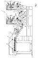
- FIGS. 1 to 7 are mutually corresponding components and elements designated by the same reference numerals.
- FIG. 1 a sheet-fed printing machine 1 with printing units 2, 3 and a boom 4 is shown.
- the sheet-fed printing machine 1 is a perfector and comprises sheet transport cylinders 5 to 7, each with at least one gripper system 8.
- the sheet transport cylinders 5, 6 are impression cylinders of the printing units 2, 3.
- the sheet transport cylinder 7 is a transfer cylinder.
- the boom 4 comprises a chain conveyor 9 with gripper systems 10.
- the chain conveyor 9 revolves around a so-called delivery drum 11.
- the sheet transport cylinders 5, 7 together form a transfer area 12, in which the printing material sheet 13 is transferred from the gripper system 8 of the sheet transport cylinder 5 into the gripper system 8 of the sheet transport cylinder 7.
- the sheet transport cylinder 6 forms, together with the chain conveyor 9, a further transfer area 15, in which the printing material sheet 13 is transferred from the gripper system 8 of the sheet transport cylinder 6 into one of the gripper systems 10 of the chain conveyor 9.
- a sheet guiding device 16 is arranged, which has a the transfer area 12 to be located end 17.
- a sheet guiding device 18 is arranged, which has an end 19 to the transfer area 15.
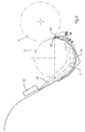
- FIG. 2 a substantially cup-shaped sheet guiding device with a comb-shaped edge 20 is shown.
- This sheet guide can the sheet guide 16 from FIG. 1 be, with the comb-shaped edge 20 is the end 17, and may also the sheet guiding device 18 from FIG. 1 be with the comb-shaped edge 20 is the end 19.
- the sheet guiding device has a concave guide surface 21 with blowing air nozzles 22.
- the comb-shaped edge 20 has tines 23 and intervening gaps 24.
- the grippers of the gripper system 8 of the sheet transport cylinder 6 or 7 go through the gaps 24 during the cylinder rotation. Close to the comb-shaped edge 20, an unloading device 25 for eliminating electrostatic charges of the printing material sheets 13 is arranged.
- the unloading device 25 is a so-called active unloading device, whose "deelectrification" serving conductor, the ionizer, is connected to a high voltage source generating an alternating high voltage.
- the discharge device 25 is a so-called anti-static bar or ionization bar.
- the comb-shaped edge 20 and in particular its tines 23 consist at least partially of a substantially electrically non-conductive material, preferably a plastic such. As polyacetal (POM) or polyphenylene sulfide (PPS). The electrical insulation effect of this material ensures a high efficiency of the unloading device 25.
- the discharged from the unloading 25 printing material sheet 13 no longer tend to smear fresh ink to the guide surface 21, since these discharged printing material 13 have no more static charges, which otherwise sticking the printing material 13 would cause on the guide surface 21.
- the sheet guiding device FIG. 2 consists of a first part 26 and a second part 27.
- the first part 26 is a blow box and the second part 27 is the comb-shaped edge 20.
- the second part 27 is formed as an attachment element, which is connected to the first part 26 via screws.
- the second part 27 is formed as a separate element, which, although rests against the first part 26, but is not connected to the latter. Instead, in this case the second part 27 is attached via a holder 28 to a blowing device 29, which in turn is attached via a further holder 30 on the machine frame 31.
- the first part 26 consists at least largely of an electrically conductive material, preferably of a metal.
- the guide surface 21 may be made of a steel sheet.
- FIG. 5 the case is shown in which the sheet guiding device FIG. 2 the delivery drum 11 is assigned. It is irrelevant whether the sheet guiding device 18 according to FIG. 3 as an attachment or according to FIG. 4 is designed as a separate element.
- a UV dryer 32 emits UV radiation 33 provided on the printing material sheet 13 for drying the printing ink, which UV radiation 33 partly reaches the interior of the skeleton-shaped delivery drum 11 and is deflected and reflected by the guide surface 21 towards the comb-shaped edge 20.
- the comb-shaped edge 20 here consists of polyphenylene sulfide (PPS) or in a comparable manner to the UV radiation 33 resistant and at the same time electrically insulating material.
- PPS polyphenylene sulfide
- the UV radiation resistance of the comb-shaped edge 20 prevents its premature aging, otherwise caused by the UV radiation 33 embrittlement and the like, so that the sheet guiding device 18 despite its proximity to the UV dryer 32 is not damaged by the latter.
- the guide surface 21 and the comb-shaped edge 20 are formed together as a single part.
- This part consists of an electrically conductive material and is z. B. a steel sheet.
- the part is coated in the region of the comb-shaped edge 20 with an insulating coating 36 whose electrical conductivity with respect to the electrical conductivity of the base material, for. B. the steel sheet, is significantly lower.
- FIG. 7 shows that in the region of ionizer tips 34 of the discharge device 25 in the guide surface 21 breakthroughs 35 are introduced, through which the ionizer tips 34 act on the printing material sheet 13.
Landscapes
- Engineering & Computer Science (AREA)
- Mechanical Engineering (AREA)
- Feeding Of Articles By Means Other Than Belts Or Rollers (AREA)
- Supply, Installation And Extraction Of Printed Sheets Or Plates (AREA)
- Elimination Of Static Electricity (AREA)
- Paper Feeding For Electrophotography (AREA)
Abstract
Description
Die vorliegende Erfindung bezieht sich auf eine Druckmaschine, mit einer Bogenleiteinrichtung, die einen Rand aufweist, nach dem Oberbegriff des Anspruchs 1.The present invention relates to a printing press, with a sheet guiding device having an edge, according to the preamble of claim 1.
In
Deshalb liegt der Erfindung die Aufgabe zugrunde, eine der eingangs genannten Gattung entsprechende Druckmaschine zu schaffen, bei welcher günstige Voraussetzungen für ein beidseitiges Bedrucken der Bogen gegeben sind.The invention is therefore an object of the invention to provide a type of printing machine corresponding to the type mentioned, in which favorable conditions for a double-sided printing of the sheet are given.
Diese Aufgabe wird durch eine Druckmaschine mit den Merkmalen des Anspruchs 1 gelöst.This object is achieved by a printing machine with the features of claim 1.
Besagtes Material, welches ein elektrischer Isolator ist, ermöglicht es, im Bereich des Randes die Entladeeinrichtung zum Entladen der Bedruckstoffbogen anzuordnen. Mittels einer solchen Entladeeinrichtung lassen sich die elektrostatischen Aufladungen des Bedruckstoffbogens bei dessen Einlauf in den Bereich der Bogenleiteinrichtung zumindest so stark reduzieren, dass der Bedruckstoffbogen infolgedessen nicht mehr dazu neigt, von der Bogenleiteinrichtung elektrostatisch angezogen zu werden und mit seiner beim Schön- und Wiederdruck der Bogenleiteinrichtung zugewandten Schöndruckseite an der Bogenleiteinrichtung abzuschmieren.Said material, which is an electrical insulator, makes it possible to arrange the unloading device for unloading the printing material in the region of the edge. By means of such an unloading device, the electrostatic charges of the printing material at its entry into the area of the sheet guiding device can be at least reduced so much that the printing sheet consequently no longer tends to be electrostatically attracted to the sheet guiding device and with its beautiful and re-printing the sheet guiding device To lubricate facing Perfecting page on the sheet guiding device.
Bei einer weiteren Weiterbildung besteht die Bogenleiteinrichtung überwiegend aus einem elektrisch leitfähigen Material. Bei weiteren Weiterbildungen ist das elektrisch im Wesentlichen nicht leitfähige Material Polyphenylensulfid oder Polyacetal.In a further development, the sheet guiding device consists predominantly of an electrically conductive material. In further developments, the electrically substantially non-conductive material is polyphenylene sulfide or polyacetal.
Bei einer weiteren Weiterbildung ist der Rand kammförmig und längserstreckt er sich quer relativ zu einer Bogenlaufrichtung der Bedruckstoffbogen.In a further development, the edge is comb-shaped and extends longitudinally transversely relative to a sheet travel direction of the printing material.
Weitere Weiterbildungen ergeben sich aus der nachfolgenden Beschreibung bevorzugter Ausführungsbeispiele und der dazugehörigen Zeichnung.Further developments will become apparent from the following description of preferred embodiments and the accompanying drawings.
In dieser zeigen:
- Figur 1
- eine Schön- und Wiederdruck-Offsetdruckmaschine mit Bogenleiteinrichtungen,
- Figur 2
- eine dreidimensionale Darstellung einer der Bogenleiteinrichtungen aus
Figur 1 , Figur 3- die Bogenleiteinrichtung aus
Figur 2 in einer Seitenansicht, Figur 4- eine Modifikation der Bogenleiteinrichtung aus
Figur 3 - Figur 5
- die Bogenleiteinrichtung aus
Figur 4 - Figur 6
- ein Ausführungsbeispiel, bei dem eine der Bogenleiteinrichtungen aus
Figur 1 ein mit einem kammförmigen Rand versehenes Düsenblech aufweist, und Figur 7- eine Detaildarstellung des kammförmigen Randes der Bogenleiteinrichtung aus
Figur 6 und einer in unmittelbarer Nähe des kammförmigen Randes angeordneten Entladeeinrichtung.
- FIG. 1
- a perfecting and reprinting offset printing machine with sheet guiding devices,
- FIG. 2
- a three-dimensional representation of one of the sheet guiding devices
FIG. 1 . - FIG. 3
- the sheet guiding device
FIG. 2 in a side view, - FIG. 4
- a modification of the sheet guiding device
FIG. 3 , with respect to the latter changed attachment of a comb-shaped edge element of the sheet guiding device, - FIG. 5
- the sheet guiding device
FIG. 4 together with a UV dryer located in the immediate vicinity, - FIG. 6
- an embodiment in which one of the sheet guiding devices
FIG. 1 a nozzle plate provided with a comb-shaped edge, and - FIG. 7
- a detailed representation of the comb-shaped edge of the sheet guiding device
FIG. 6 and an unloading device arranged in the immediate vicinity of the comb-shaped edge.
In den
In
In
In den
Gemäß
Gemäß
Sowohl bei dem in
In
Bei dem in den
Zeichnerisch nicht dargestellt sind Modifikationen der in den
- 11
- BogendruckmaschineSheetfed
- 22
- Druckwerkprinting unit
- 33
- Druckwerkprinting unit
- 44
- Auslegerboom
- 55
- BogentransportzylinderSheet transfer cylinders
- 66
- BogentransportzylinderSheet transfer cylinders
- 77
- BogentransportzylinderSheet transfer cylinders
- 88th
- Greifersystemgripper system
- 99
- Kettenfördererchain conveyors
- 1010
- Greifersystemgripper system
- 1111
- Auslagetrommeldelivery drum
- 1212
- ÜbergabebereichTransfer area
- 1313
- Bedruckstoffbogenprinting material
- 1414
- ./../.
- 1515
- ÜbergabebereichTransfer area
- 1616
- Bogenleiteinrichtungsheet guiding device
- 1717
- EndeThe End
- 1818
- Bogenleiteinrichtungsheet guiding device
- 1919
- EndeThe End
- 2020
- kammförmiger Randcomb-shaped edge
- 2121
- Leitflächebaffle
- 2222
- Luftdüseair nozzle
- 2323
- Zinkenprong
- 2424
- Lückegap
- 2525
- Entladeeinrichtungunloading
- 2626
- erstes Teilfirst part
- 2727
- zweites Teilsecond part
- 2828
- Halterholder
- 2929
- Blaseinrichtungblower
- 3030
- Halterholder
- 3131
- Maschinengestellmachine frame
- 3232
- UV-TrocknerUV dryer
- 3333
- UV-StrahlungUV radiation
- 3434
- IonisatorspitzeIonisatorspitze
- 3535
- Durchbruchbreakthrough
- 3636
- Isolierbeschichtunginsulating
Claims (6)
- Printing press (1) having a sheet-guiding device (16, 18) with an edge (20) at least partly consisting of a material that is essentially electrically non-conductive,
characterized by
the fact that in the region of the edge (20), a discharge device (25) is arranged to discharge the sheets (13) of printing material. - Printing press according to Claim 1,
characterized by
the fact that the sheet-guiding device (16, 18) predominantly consists of an electrically conductive material. - Printing press according to Claim 1 or 2,
characterized by
the fact that the material that is essentially electrically non-conductive is polyphenylene sulfide. - Printing press according to one of Claims 1 or 2,
characterized by
the fact that the material that is essentially electrically non-conductive is polyacetal. - Printing press according to one of Claims 1 to 4,
characterized by
the fact that transversely, the edge (20) extends in a longitudinal direction relative to the direction of travel of the sheets (13) of printing material. - Printing press according to one of Claims 1 to 5,
characterized by
the fact that the edge (20) is a comb-shaped edge (20).
Applications Claiming Priority (2)
| Application Number | Priority Date | Filing Date | Title |
|---|---|---|---|
| DE102005000892 | 2005-01-07 | ||
| DE102005032601A DE102005032601A1 (en) | 2005-01-07 | 2005-07-13 | press |
Publications (3)
| Publication Number | Publication Date |
|---|---|
| EP1679187A2 EP1679187A2 (en) | 2006-07-12 |
| EP1679187A3 EP1679187A3 (en) | 2010-03-03 |
| EP1679187B1 true EP1679187B1 (en) | 2011-05-25 |
Family
ID=35907019
Family Applications (1)
| Application Number | Title | Priority Date | Filing Date |
|---|---|---|---|
| EP05112187A Active EP1679187B1 (en) | 2005-01-07 | 2005-12-15 | Sheet guiding device with electric isolating comb like border |
Country Status (6)
| Country | Link |
|---|---|
| US (1) | US20060150841A1 (en) |
| EP (1) | EP1679187B1 (en) |
| JP (1) | JP4833667B2 (en) |
| CN (1) | CN1799839B (en) |
| AT (1) | ATE510693T1 (en) |
| DE (1) | DE102005032601A1 (en) |
Cited By (5)
| Publication number | Priority date | Publication date | Assignee | Title |
|---|---|---|---|---|
| DE102019118569A1 (en) * | 2019-07-09 | 2021-01-14 | Koenig & Bauer Ag | Sheet processing machine and method for conveying sheets |
| WO2021004696A1 (en) | 2019-07-09 | 2021-01-14 | Koenig & Bauer Ag | Sheet-processing machine with a turning device, method for conveying sheets, and use of sheet directing elements which contain deionization devices |
| DE102019118565A1 (en) * | 2019-07-09 | 2021-01-14 | Koenig & Bauer Ag | Sheet processing machine and method for conveying sheets |
| DE102019118566A1 (en) * | 2019-07-09 | 2021-01-14 | Koenig & Bauer Ag | Sheet processing machine and method for conveying sheets |
| DE102019118571A1 (en) * | 2019-07-09 | 2021-01-14 | Koenig & Bauer Ag | Sheet processing machine and method for conveying sheets |
Families Citing this family (6)
| Publication number | Priority date | Publication date | Assignee | Title |
|---|---|---|---|---|
| DE102008009156B4 (en) | 2007-02-23 | 2018-11-08 | Heidelberger Druckmaschinen Ag | Arrangement for dissipating electrostatic charges from a substrate |
| DE102008034766A1 (en) * | 2008-07-25 | 2010-01-28 | Heidelberger Druckmaschinen Ag | Sheet guiding element made of antistatic plastic |
| DE102010028595B4 (en) * | 2010-05-05 | 2021-06-10 | manroland sheetfed GmbH | Sheet processing machine with comb-shaped sheet guiding device |
| US8462480B2 (en) * | 2010-05-26 | 2013-06-11 | Illinois Tool Works Inc. | In-line gas ionizer with static dissipative material and counterelectrode |
| DE102022104772A1 (en) | 2022-03-01 | 2023-09-07 | Heidelberger Druckmaschinen Aktiengesellschaft | Device for guiding printed sheets in a printing machine |
| DE102023103112B3 (en) | 2023-02-09 | 2023-12-14 | Heidelberger Druckmaschinen Aktiengesellschaft | Device for guiding sheets in a printing press |
Family Cites Families (108)
| Publication number | Priority date | Publication date | Assignee | Title |
|---|---|---|---|---|
| US3495269A (en) * | 1966-12-19 | 1970-02-10 | Xerox Corp | Electrographic recording method and apparatus with inert gaseous discharge ionization and acceleration gaps |
| US3496352A (en) * | 1967-06-05 | 1970-02-17 | Xerox Corp | Self-cleaning corona generating apparatus |
| JPS5130491A (en) * | 1974-09-09 | 1976-03-15 | Kasuga Electric Co | SEIDENKIJOKYOSOCHODENKYOKU |
| US4015203A (en) * | 1975-12-31 | 1977-03-29 | International Business Machines Corporation | Contactless LSI junction leakage testing method |
| US4247203A (en) * | 1978-04-03 | 1981-01-27 | Kla Instrument Corporation | Automatic photomask inspection system and apparatus |
| US4440082A (en) * | 1978-11-13 | 1984-04-03 | Dayco Corporation | Electrostatically assisted printing system |
| US4378159A (en) * | 1981-03-30 | 1983-03-29 | Tencor Instruments | Scanning contaminant and defect detector |
| US4448532A (en) * | 1981-03-31 | 1984-05-15 | Kla Instruments Corporation | Automatic photomask inspection method and system |
| US4926489A (en) * | 1983-03-11 | 1990-05-15 | Kla Instruments Corporation | Reticle inspection system |
| US4579455A (en) * | 1983-05-09 | 1986-04-01 | Kla Instruments Corporation | Photomask inspection apparatus and method with improved defect detection |
| US4578810A (en) * | 1983-08-08 | 1986-03-25 | Itek Corporation | System for printed circuit board defect detection |
| JPS6062122A (en) * | 1983-09-16 | 1985-04-10 | Fujitsu Ltd | Inspection of mask pattern |
| US4595289A (en) * | 1984-01-25 | 1986-06-17 | At&T Bell Laboratories | Inspection system utilizing dark-field illumination |
| US4580775A (en) * | 1984-03-02 | 1986-04-08 | Ikegani Tsushinki Company, Ltd. | Sheet sorting apparatus |
| JPS60263807A (en) * | 1984-06-12 | 1985-12-27 | Dainippon Screen Mfg Co Ltd | Instument for inspecting pattern defect of printed wiring board |
| US4817123A (en) * | 1984-09-21 | 1989-03-28 | Picker International | Digital radiography detector resolution improvement |
| US4734721A (en) * | 1985-10-04 | 1988-03-29 | Markem Corporation | Electrostatic printer utilizing dehumidified air |
| US4641967A (en) * | 1985-10-11 | 1987-02-10 | Tencor Instruments | Particle position correlator and correlation method for a surface scanner |
| US4928313A (en) * | 1985-10-25 | 1990-05-22 | Synthetic Vision Systems, Inc. | Method and system for automatically visually inspecting an article |
| DE3601660A1 (en) * | 1986-01-21 | 1987-07-23 | Eltex Elektrostatik Gmbh | METHOD AND DEVICE FOR FOLDING SHEETS CUT FROM A CONTINUOUS MATERIAL |
| US4814829A (en) * | 1986-06-12 | 1989-03-21 | Canon Kabushiki Kaisha | Projection exposure apparatus |
| US4805123B1 (en) * | 1986-07-14 | 1998-10-13 | Kla Instr Corp | Automatic photomask and reticle inspection method and apparatus including improved defect detector and alignment sub-systems |
| US4812756A (en) * | 1987-08-26 | 1989-03-14 | International Business Machines Corporation | Contactless technique for semicondutor wafer testing |
| JP3707172B2 (en) * | 1996-01-24 | 2005-10-19 | 富士ゼロックス株式会社 | Image reading device |
| US5205217A (en) * | 1990-12-31 | 1993-04-27 | Howard W. DeMoore | Vacuum transfer apparatus for rotary sheet-fed printing presses |
| JPH04312796A (en) * | 1991-04-10 | 1992-11-04 | Kitagawa Ind Co Ltd | Ion generating apparatus for electric charge prevention |
| US5189481A (en) * | 1991-07-26 | 1993-02-23 | Tencor Instruments | Particle detector for rough surfaces |
| US5563702A (en) * | 1991-08-22 | 1996-10-08 | Kla Instruments Corporation | Automated photomask inspection apparatus and method |
| DE69208413T2 (en) * | 1991-08-22 | 1996-11-14 | Kla Instr Corp | Device for automatic testing of photomask |
| JP2512258B2 (en) * | 1992-03-11 | 1996-07-03 | 松下電器産業株式会社 | Sheet feeding device |
| JP2667940B2 (en) * | 1992-04-27 | 1997-10-27 | 三菱電機株式会社 | Mask inspection method and mask detection device |
| US5448053A (en) * | 1993-03-01 | 1995-09-05 | Rhoads; Geoffrey B. | Method and apparatus for wide field distortion-compensated imaging |
| US5500607A (en) * | 1993-12-22 | 1996-03-19 | International Business Machines Corporation | Probe-oxide-semiconductor method and apparatus for measuring oxide charge on a semiconductor wafer |
| US5572608A (en) * | 1994-08-24 | 1996-11-05 | International Business Machines Corporation | Sinc filter in linear lumen space for scanner |
| US5608538A (en) * | 1994-08-24 | 1997-03-04 | International Business Machines Corporation | Scan line queuing for high performance image correction |
| US5528153A (en) * | 1994-11-07 | 1996-06-18 | Texas Instruments Incorporated | Method for non-destructive, non-contact measurement of dielectric constant of thin films |
| CA2139182A1 (en) * | 1994-12-28 | 1996-06-29 | Paul Chevrette | Method and system for fast microscanning |
| US5485091A (en) * | 1995-05-12 | 1996-01-16 | International Business Machines Corporation | Contactless electrical thin oxide measurements |
| US6288780B1 (en) * | 1995-06-06 | 2001-09-11 | Kla-Tencor Technologies Corp. | High throughput brightfield/darkfield wafer inspection system using advanced optical techniques |
| US5594247A (en) * | 1995-07-07 | 1997-01-14 | Keithley Instruments, Inc. | Apparatus and method for depositing charge on a semiconductor wafer |
| JPH0919999A (en) * | 1995-07-07 | 1997-01-21 | Toray Ind Inc | Printing machine with static eliminator and printing method therefor |
| US5773989A (en) * | 1995-07-14 | 1998-06-30 | University Of South Florida | Measurement of the mobile ion concentration in the oxide layer of a semiconductor wafer |
| US5621519A (en) * | 1995-07-31 | 1997-04-15 | Neopath, Inc. | Imaging system transfer function control method and apparatus |
| US5619548A (en) * | 1995-08-11 | 1997-04-08 | Oryx Instruments And Materials Corp. | X-ray thickness gauge |
| US5754678A (en) * | 1996-01-17 | 1998-05-19 | Photon Dynamics, Inc. | Substrate inspection apparatus and method |
| US5742658A (en) * | 1996-05-23 | 1998-04-21 | Advanced Micro Devices, Inc. | Apparatus and method for determining the elemental compositions and relative locations of particles on the surface of a semiconductor wafer |
| US5767693A (en) * | 1996-09-04 | 1998-06-16 | Smithley Instruments, Inc. | Method and apparatus for measurement of mobile charges with a corona screen gun |
| US6076465A (en) * | 1996-09-20 | 2000-06-20 | Kla-Tencor Corporation | System and method for determining reticle defect printability |
| KR100200734B1 (en) * | 1996-10-10 | 1999-06-15 | 윤종용 | Measuring apparatus and method of aerial image |
| US5866806A (en) * | 1996-10-11 | 1999-02-02 | Kla-Tencor Corporation | System for locating a feature of a surface |
| US5928389A (en) * | 1996-10-21 | 1999-07-27 | Applied Materials, Inc. | Method and apparatus for priority based scheduling of wafer processing within a multiple chamber semiconductor wafer processing tool |
| DE29702626U1 (en) * | 1997-02-15 | 1997-04-03 | MAN Roland Druckmaschinen AG, 63075 Offenbach | Dust removal system with sheet guiding device |
| US5889593A (en) * | 1997-02-26 | 1999-03-30 | Kla Instruments Corporation | Optical system and method for angle-dependent reflection or transmission measurement |
| US6097196A (en) * | 1997-04-23 | 2000-08-01 | Verkuil; Roger L. | Non-contact tunnelling field measurement for a semiconductor oxide layer |
| US6078738A (en) * | 1997-05-08 | 2000-06-20 | Lsi Logic Corporation | Comparing aerial image to SEM of photoresist or substrate pattern for masking process characterization |
| US6201999B1 (en) * | 1997-06-09 | 2001-03-13 | Applied Materials, Inc. | Method and apparatus for automatically generating schedules for wafer processing within a multichamber semiconductor wafer processing tool |
| US6011404A (en) * | 1997-07-03 | 2000-01-04 | Lucent Technologies Inc. | System and method for determining near--surface lifetimes and the tunneling field of a dielectric in a semiconductor |
| US6072320A (en) * | 1997-07-30 | 2000-06-06 | Verkuil; Roger L. | Product wafer junction leakage measurement using light and eddy current |
| US6191605B1 (en) * | 1997-08-18 | 2001-02-20 | Tom G. Miller | Contactless method for measuring total charge of an insulating layer on a substrate using corona charge |
| JP3671617B2 (en) * | 1997-09-01 | 2005-07-13 | コニカミノルタホールディングス株式会社 | Image forming apparatus |
| US6757645B2 (en) * | 1997-09-17 | 2004-06-29 | Numerical Technologies, Inc. | Visual inspection and verification system |
| US7107571B2 (en) * | 1997-09-17 | 2006-09-12 | Synopsys, Inc. | Visual analysis and verification system using advanced tools |
| US5874733A (en) * | 1997-10-16 | 1999-02-23 | Raytheon Company | Convergent beam scanner linearizing method and apparatus |
| US6233719B1 (en) * | 1997-10-27 | 2001-05-15 | Kla-Tencor Corporation | System and method for analyzing semiconductor production data |
| JPH11207927A (en) * | 1997-11-05 | 1999-08-03 | Heidelberger Druckmas Ag | Reversing device with linear driver for sheet-feed rotary press |
| DE29720989U1 (en) | 1997-11-27 | 1998-01-08 | MAN Roland Druckmaschinen AG, 63075 Offenbach | Sheet guiding device with a guide surface in a printing press |
| US6060709A (en) * | 1997-12-31 | 2000-05-09 | Verkuil; Roger L. | Apparatus and method for depositing uniform charge on a thin oxide semiconductor wafer |
| US6175645B1 (en) * | 1998-01-22 | 2001-01-16 | Applied Materials, Inc. | Optical inspection method and apparatus |
| US6171737B1 (en) * | 1998-02-03 | 2001-01-09 | Advanced Micro Devices, Inc. | Low cost application of oxide test wafer for defect monitor in photolithography process |
| US6324298B1 (en) * | 1998-07-15 | 2001-11-27 | August Technology Corp. | Automated wafer defect inspection system and a process of performing such inspection |
| US6466314B1 (en) * | 1998-09-17 | 2002-10-15 | Applied Materials, Inc. | Reticle design inspection system |
| US6535628B2 (en) * | 1998-10-15 | 2003-03-18 | Applied Materials, Inc. | Detection of wafer fragments in a wafer processing apparatus |
| US6842225B1 (en) * | 1999-05-07 | 2005-01-11 | Nikon Corporation | Exposure apparatus, microdevice, photomask, method of exposure, and method of production of device |
| JP2002544555A (en) * | 1999-05-18 | 2002-12-24 | アプライド マテリアルズ インコーポレイテッド | Method and apparatus for inspecting articles by comparison with a master |
| FR2801673B1 (en) * | 1999-11-26 | 2001-12-28 | Pechiney Aluminium | METHOD FOR MEASURING THE DEGREE AND THE HOMOGENEITY OF CALCINATION OF ALUMINS |
| US7190292B2 (en) * | 1999-11-29 | 2007-03-13 | Bizjak Karl M | Input level adjust system and method |
| US6701004B1 (en) * | 1999-12-22 | 2004-03-02 | Intel Corporation | Detecting defects on photomasks |
| US6569691B1 (en) * | 2000-03-29 | 2003-05-27 | Semiconductor Diagnostics, Inc. | Measurement of different mobile ion concentrations in the oxide layer of a semiconductor wafer |
| DE10023841B4 (en) * | 2000-05-16 | 2004-05-06 | Manfred Rachner Gmbh | Turning device for single stacks consisting of individual sheets |
| JP3833050B2 (en) * | 2000-05-17 | 2006-10-11 | キヤノン株式会社 | Image forming apparatus |
| EP1296351A4 (en) * | 2000-06-27 | 2009-09-23 | Ebara Corp | Charged particle beam inspection apparatus and method for fabricating device using that inspection apparatus |
| US6513151B1 (en) * | 2000-09-14 | 2003-01-28 | Advanced Micro Devices, Inc. | Full flow focus exposure matrix analysis and electrical testing for new product mask evaluation |
| US6680621B2 (en) * | 2001-01-26 | 2004-01-20 | Semiconductor Diagnostics, Inc. | Steady state method for measuring the thickness and the capacitance of ultra thin dielectric in the presence of substantial leakage current |
| JP4199939B2 (en) * | 2001-04-27 | 2008-12-24 | 株式会社日立製作所 | Semiconductor inspection system |
| KR100845067B1 (en) * | 2001-09-12 | 2008-07-09 | 마쯔시다덴기산교 가부시키가이샤 | Image coding method and image decoding method |
| JP3955450B2 (en) * | 2001-09-27 | 2007-08-08 | 株式会社ルネサステクノロジ | Sample inspection method |
| US6734696B2 (en) * | 2001-11-01 | 2004-05-11 | Kla-Tencor Technologies Corp. | Non-contact hysteresis measurements of insulating films |
| EP1352738A3 (en) * | 2002-04-08 | 2004-08-04 | Komori Corporation | Sheet guide apparatus |
| JP2004031709A (en) * | 2002-06-27 | 2004-01-29 | Seiko Instruments Inc | Waferless measuring recipe generating system |
| US7012438B1 (en) * | 2002-07-10 | 2006-03-14 | Kla-Tencor Technologies Corp. | Methods and systems for determining a property of an insulating film |
| US7418124B2 (en) * | 2002-07-15 | 2008-08-26 | Kla-Tencor Technologies Corp. | Qualifying patterns, patterning processes, or patterning apparatus in the fabrication of microlithographic patterns |
| US7338619B2 (en) * | 2002-07-22 | 2008-03-04 | Toyoda Gosei Co., Ltd. | Resin member and method of manufacturing the same |
| JP2004069884A (en) * | 2002-08-05 | 2004-03-04 | Brother Ind Ltd | Image forming apparatus equipped with image reading means |
| US7043071B2 (en) * | 2002-09-13 | 2006-05-09 | Synopsys, Inc. | Soft defect printability simulation and analysis for masks |
| KR100474571B1 (en) * | 2002-09-23 | 2005-03-10 | 삼성전자주식회사 | Method of setting reference images, method and apparatus using the setting method for inspecting patterns on a wafer |
| US7379175B1 (en) * | 2002-10-15 | 2008-05-27 | Kla-Tencor Technologies Corp. | Methods and systems for reticle inspection and defect review using aerial imaging |
| US7027143B1 (en) * | 2002-10-15 | 2006-04-11 | Kla-Tencor Technologies Corp. | Methods and systems for inspecting reticles using aerial imaging at off-stepper wavelengths |
| US6807503B2 (en) * | 2002-11-04 | 2004-10-19 | Brion Technologies, Inc. | Method and apparatus for monitoring integrated circuit fabrication |
| US7457736B2 (en) * | 2002-11-21 | 2008-11-25 | Synopsys, Inc. | Automated creation of metrology recipes |
| JP4144366B2 (en) * | 2003-02-10 | 2008-09-03 | ブラザー工業株式会社 | Thermal fixing device and image forming apparatus |
| US7053355B2 (en) * | 2003-03-18 | 2006-05-30 | Brion Technologies, Inc. | System and method for lithography process monitoring and control |
| US6859746B1 (en) * | 2003-05-01 | 2005-02-22 | Advanced Micro Devices, Inc. | Methods of using adaptive sampling techniques based upon categorization of process variations, and system for performing same |
| US7135344B2 (en) * | 2003-07-11 | 2006-11-14 | Applied Materials, Israel, Ltd. | Design-based monitoring |
| US6988045B2 (en) * | 2003-08-04 | 2006-01-17 | Advanced Micro Devices, Inc. | Dynamic metrology sampling methods, and system for performing same |
| CN101027693B (en) * | 2004-08-09 | 2010-05-12 | 伯拉考国际股份公司 | An image registration method and apparatus for medical imaging based on mulptiple masks |
| US7310796B2 (en) * | 2004-08-27 | 2007-12-18 | Applied Materials, Israel, Ltd. | System and method for simulating an aerial image |
| DE102004058377A1 (en) * | 2004-12-03 | 2006-06-14 | Man Roland Druckmaschinen Ag | Sheet guiding device for a sheet-processing machine, in particular rotary printing press |
| US20070002322A1 (en) * | 2005-06-30 | 2007-01-04 | Yan Borodovsky | Image inspection method |
-
2005
- 2005-07-13 DE DE102005032601A patent/DE102005032601A1/en not_active Withdrawn
- 2005-12-15 EP EP05112187A patent/EP1679187B1/en active Active
- 2005-12-15 AT AT05112187T patent/ATE510693T1/en active
-
2006
- 2006-01-06 CN CN2006100057838A patent/CN1799839B/en active Active
- 2006-01-09 US US11/328,414 patent/US20060150841A1/en not_active Abandoned
- 2006-01-10 JP JP2006002300A patent/JP4833667B2/en active Active
Cited By (14)
| Publication number | Priority date | Publication date | Assignee | Title |
|---|---|---|---|---|
| DE102019118569A1 (en) * | 2019-07-09 | 2021-01-14 | Koenig & Bauer Ag | Sheet processing machine and method for conveying sheets |
| WO2021004696A1 (en) | 2019-07-09 | 2021-01-14 | Koenig & Bauer Ag | Sheet-processing machine with a turning device, method for conveying sheets, and use of sheet directing elements which contain deionization devices |
| DE102019118565A1 (en) * | 2019-07-09 | 2021-01-14 | Koenig & Bauer Ag | Sheet processing machine and method for conveying sheets |
| DE102019118566A1 (en) * | 2019-07-09 | 2021-01-14 | Koenig & Bauer Ag | Sheet processing machine and method for conveying sheets |
| DE102019118571A1 (en) * | 2019-07-09 | 2021-01-14 | Koenig & Bauer Ag | Sheet processing machine and method for conveying sheets |
| DE102019118569B4 (en) | 2019-07-09 | 2022-05-12 | Koenig & Bauer Ag | Sheet processing machine and method for conveying sheets |
| DE102019118571B4 (en) | 2019-07-09 | 2022-05-25 | Koenig & Bauer Ag | Sheet processing machine and method for conveying sheets |
| DE102019118566B4 (en) | 2019-07-09 | 2022-07-14 | Koenig & Bauer Ag | Sheet processing machine and method for conveying sheets |
| DE102019118565B4 (en) | 2019-07-09 | 2022-07-21 | Koenig & Bauer Ag | Sheet processing machine and method for conveying sheets |
| US11498790B2 (en) | 2019-07-09 | 2022-11-15 | Koenig & Bauer Ag | Sheet-processing machine comprising a turning device, method for conveying sheets, and use of sheet guide elements containing deionization devices |
| EP4209351A1 (en) | 2019-07-09 | 2023-07-12 | Koenig & Bauer AG | Sheet processing machine, use of the sheet processing machine, method for conveying sheets and use of sheet guiding elements containing deionization devices |
| EP4209349A1 (en) | 2019-07-09 | 2023-07-12 | Koenig & Bauer AG | Sheet processing machine, use of the sheet processing machine, method for conveying sheets and use of sheet guiding elements containing deionization devices |
| EP4209350A1 (en) | 2019-07-09 | 2023-07-12 | Koenig & Bauer AG | Sheet processing machine, use of the sheet processing machine and method for conveying sheets |
| EP4209352A1 (en) | 2019-07-09 | 2023-07-12 | Koenig & Bauer AG | Sheet processing machine, use of the sheet processing machine, method for conveying sheets and use of sheet guiding elements containing deionization devices |
Also Published As
| Publication number | Publication date |
|---|---|
| JP4833667B2 (en) | 2011-12-07 |
| EP1679187A2 (en) | 2006-07-12 |
| CN1799839A (en) | 2006-07-12 |
| CN1799839B (en) | 2012-03-07 |
| EP1679187A3 (en) | 2010-03-03 |
| ATE510693T1 (en) | 2011-06-15 |
| JP2006188065A (en) | 2006-07-20 |
| DE102005032601A1 (en) | 2006-07-20 |
| US20060150841A1 (en) | 2006-07-13 |
Similar Documents
| Publication | Publication Date | Title |
|---|---|---|
| EP1679187B1 (en) | Sheet guiding device with electric isolating comb like border | |
| EP1117487B1 (en) | Coating machine for upgrading sheet material | |
| EP0306682B1 (en) | Device for conveying sheets through the printing zone between the offset cylinder and the impression cylinder in a rotary sheet-fed printing press | |
| EP1105295B1 (en) | Device for powdering printed sheets with the aid of an electrostatic charge | |
| DE19857984A1 (en) | Drying station for printed sheets at a sheet-fed offset printing press has a hood containing the radiator and inert gas blower with cylinders at the hood entry and exit to prevent gas escape | |
| DE102004011114B4 (en) | Bedruckstoffverarbeitungsmaschine | |
| EP1418049B1 (en) | Rotary printing machine | |
| DE102008009156B4 (en) | Arrangement for dissipating electrostatic charges from a substrate | |
| DE19829095C2 (en) | Sheet guiding device in a printing press | |
| EP1303407A1 (en) | Drying installation within a sheet-fed printing press | |
| DE102012218048B4 (en) | Sheet transport drum, use of changeable coatings on respective tines of casing segments of a sheet transport drum and method for adjusting contact properties of a sheet transport drum | |
| DE20113639U1 (en) | Coating machine for finishing printed sheets | |
| EP3863855B1 (en) | Device, method and printing press for multiple printing of printing sheets | |
| DE10157566B4 (en) | Sheet guiding device with a guide surface in a printing machine | |
| CH651501A5 (en) | Sheet-fed rotary printing machine having at least one printing unit | |
| WO1998007568A1 (en) | Device for dusting moving objects, including printed paper sheets | |
| DE19611590C1 (en) | Sheet guiding drum for a printing machine | |
| DE102010028702B4 (en) | Turning device of a sheet-fed printing machine | |
| EP1040061B1 (en) | Device for influencing signatures by electrostatic means | |
| DE102014224896A1 (en) | Sheet processing machine and method for painting the sheet front pages and / or the sheet backs | |
| DE102010028698A1 (en) | Sheet guide device e.g. storage drum, for use as e.g. feeder, in e.g. sheet fed press, has guide surface for guiding electrical charged printed sheets, where guide surface is provided with smooth and rough portions with different roughness | |
| DE102010028701B4 (en) | Sheet guiding device | |
| DE10315173B4 (en) | Printing cylinder for metal sheet printing machines and the like | |
| DE19958631A1 (en) | Sheetfed offset printing machine | |
| EP1129849B1 (en) | Endless-chain sheet feeder |
Legal Events
| Date | Code | Title | Description |
|---|---|---|---|
| PUAI | Public reference made under article 153(3) epc to a published international application that has entered the european phase |
Free format text: ORIGINAL CODE: 0009012 |
|
| AK | Designated contracting states |
Kind code of ref document: A2 Designated state(s): AT BE BG CH CY CZ DE DK EE ES FI FR GB GR HU IE IS IT LI LT LU LV MC NL PL PT RO SE SI SK TR |
|
| AX | Request for extension of the european patent |
Extension state: AL BA HR MK YU |
|
| PUAL | Search report despatched |
Free format text: ORIGINAL CODE: 0009013 |
|
| AK | Designated contracting states |
Kind code of ref document: A3 Designated state(s): AT BE BG CH CY CZ DE DK EE ES FI FR GB GR HU IE IS IT LI LT LU LV MC NL PL PT RO SE SI SK TR |
|
| AX | Request for extension of the european patent |
Extension state: AL BA HR MK YU |
|
| 17P | Request for examination filed |
Effective date: 20100903 |
|
| 17Q | First examination report despatched |
Effective date: 20100928 |
|
| AKX | Designation fees paid |
Designated state(s): AT BE BG CH CY CZ DE DK EE ES FI FR GB GR HU IE IS IT LI LT LU LV MC NL PL PT RO SE SI SK TR |
|
| RIC1 | Information provided on ipc code assigned before grant |
Ipc: B41F 21/00 20060101AFI20101021BHEP |
|
| GRAP | Despatch of communication of intention to grant a patent |
Free format text: ORIGINAL CODE: EPIDOSNIGR1 |
|
| GRAS | Grant fee paid |
Free format text: ORIGINAL CODE: EPIDOSNIGR3 |
|
| GRAA | (expected) grant |
Free format text: ORIGINAL CODE: 0009210 |
|
| REG | Reference to a national code |
Ref country code: DE Ref legal event code: R081 Ref document number: 502005011426 Country of ref document: DE Owner name: HEIDELBERGER DRUCKMASCHINEN AG, DE Free format text: FORMER OWNER: HEIDELBERGER DRUCKMASCHINEN AG, 69115 HEIDELBERG, DE |
|
| AK | Designated contracting states |
Kind code of ref document: B1 Designated state(s): AT BE BG CH CY CZ DE DK EE ES FI FR GB GR HU IE IS IT LI LT LU LV MC NL PL PT RO SE SI SK TR |
|
| REG | Reference to a national code |
Ref country code: GB Ref legal event code: FG4D Free format text: NOT ENGLISH |
|
| REG | Reference to a national code |
Ref country code: CH Ref legal event code: EP |
|
| REG | Reference to a national code |
Ref country code: IE Ref legal event code: FG4D Free format text: LANGUAGE OF EP DOCUMENT: GERMAN |
|
| REG | Reference to a national code |
Ref country code: DE Ref legal event code: R096 Ref document number: 502005011426 Country of ref document: DE Effective date: 20110707 |
|
| REG | Reference to a national code |
Ref country code: NL Ref legal event code: VDEP Effective date: 20110525 |
|
| PG25 | Lapsed in a contracting state [announced via postgrant information from national office to epo] |
Ref country code: PT Free format text: LAPSE BECAUSE OF FAILURE TO SUBMIT A TRANSLATION OF THE DESCRIPTION OR TO PAY THE FEE WITHIN THE PRESCRIBED TIME-LIMIT Effective date: 20110926 Ref country code: LT Free format text: LAPSE BECAUSE OF FAILURE TO SUBMIT A TRANSLATION OF THE DESCRIPTION OR TO PAY THE FEE WITHIN THE PRESCRIBED TIME-LIMIT Effective date: 20110525 Ref country code: SE Free format text: LAPSE BECAUSE OF FAILURE TO SUBMIT A TRANSLATION OF THE DESCRIPTION OR TO PAY THE FEE WITHIN THE PRESCRIBED TIME-LIMIT Effective date: 20110525 |
|
| PG25 | Lapsed in a contracting state [announced via postgrant information from national office to epo] |
Ref country code: ES Free format text: LAPSE BECAUSE OF FAILURE TO SUBMIT A TRANSLATION OF THE DESCRIPTION OR TO PAY THE FEE WITHIN THE PRESCRIBED TIME-LIMIT Effective date: 20110905 Ref country code: IS Free format text: LAPSE BECAUSE OF FAILURE TO SUBMIT A TRANSLATION OF THE DESCRIPTION OR TO PAY THE FEE WITHIN THE PRESCRIBED TIME-LIMIT Effective date: 20110925 Ref country code: LV Free format text: LAPSE BECAUSE OF FAILURE TO SUBMIT A TRANSLATION OF THE DESCRIPTION OR TO PAY THE FEE WITHIN THE PRESCRIBED TIME-LIMIT Effective date: 20110525 Ref country code: GR Free format text: LAPSE BECAUSE OF FAILURE TO SUBMIT A TRANSLATION OF THE DESCRIPTION OR TO PAY THE FEE WITHIN THE PRESCRIBED TIME-LIMIT Effective date: 20110826 Ref country code: CY Free format text: LAPSE BECAUSE OF FAILURE TO SUBMIT A TRANSLATION OF THE DESCRIPTION OR TO PAY THE FEE WITHIN THE PRESCRIBED TIME-LIMIT Effective date: 20110525 Ref country code: FI Free format text: LAPSE BECAUSE OF FAILURE TO SUBMIT A TRANSLATION OF THE DESCRIPTION OR TO PAY THE FEE WITHIN THE PRESCRIBED TIME-LIMIT Effective date: 20110525 Ref country code: SI Free format text: LAPSE BECAUSE OF FAILURE TO SUBMIT A TRANSLATION OF THE DESCRIPTION OR TO PAY THE FEE WITHIN THE PRESCRIBED TIME-LIMIT Effective date: 20110525 |
|
| REG | Reference to a national code |
Ref country code: IE Ref legal event code: FD4D |
|
| PG25 | Lapsed in a contracting state [announced via postgrant information from national office to epo] |
Ref country code: NL Free format text: LAPSE BECAUSE OF FAILURE TO SUBMIT A TRANSLATION OF THE DESCRIPTION OR TO PAY THE FEE WITHIN THE PRESCRIBED TIME-LIMIT Effective date: 20110525 |
|
| PG25 | Lapsed in a contracting state [announced via postgrant information from national office to epo] |
Ref country code: CZ Free format text: LAPSE BECAUSE OF FAILURE TO SUBMIT A TRANSLATION OF THE DESCRIPTION OR TO PAY THE FEE WITHIN THE PRESCRIBED TIME-LIMIT Effective date: 20110525 Ref country code: IE Free format text: LAPSE BECAUSE OF FAILURE TO SUBMIT A TRANSLATION OF THE DESCRIPTION OR TO PAY THE FEE WITHIN THE PRESCRIBED TIME-LIMIT Effective date: 20110525 Ref country code: EE Free format text: LAPSE BECAUSE OF FAILURE TO SUBMIT A TRANSLATION OF THE DESCRIPTION OR TO PAY THE FEE WITHIN THE PRESCRIBED TIME-LIMIT Effective date: 20110525 |
|
| PG25 | Lapsed in a contracting state [announced via postgrant information from national office to epo] |
Ref country code: PL Free format text: LAPSE BECAUSE OF FAILURE TO SUBMIT A TRANSLATION OF THE DESCRIPTION OR TO PAY THE FEE WITHIN THE PRESCRIBED TIME-LIMIT Effective date: 20110525 Ref country code: RO Free format text: LAPSE BECAUSE OF FAILURE TO SUBMIT A TRANSLATION OF THE DESCRIPTION OR TO PAY THE FEE WITHIN THE PRESCRIBED TIME-LIMIT Effective date: 20110525 Ref country code: SK Free format text: LAPSE BECAUSE OF FAILURE TO SUBMIT A TRANSLATION OF THE DESCRIPTION OR TO PAY THE FEE WITHIN THE PRESCRIBED TIME-LIMIT Effective date: 20110525 Ref country code: DK Free format text: LAPSE BECAUSE OF FAILURE TO SUBMIT A TRANSLATION OF THE DESCRIPTION OR TO PAY THE FEE WITHIN THE PRESCRIBED TIME-LIMIT Effective date: 20110525 |
|
| PLBE | No opposition filed within time limit |
Free format text: ORIGINAL CODE: 0009261 |
|
| STAA | Information on the status of an ep patent application or granted ep patent |
Free format text: STATUS: NO OPPOSITION FILED WITHIN TIME LIMIT |
|
| 26N | No opposition filed |
Effective date: 20120228 |
|
| PG25 | Lapsed in a contracting state [announced via postgrant information from national office to epo] |
Ref country code: IT Free format text: LAPSE BECAUSE OF FAILURE TO SUBMIT A TRANSLATION OF THE DESCRIPTION OR TO PAY THE FEE WITHIN THE PRESCRIBED TIME-LIMIT Effective date: 20110525 |
|
| REG | Reference to a national code |
Ref country code: DE Ref legal event code: R097 Ref document number: 502005011426 Country of ref document: DE Effective date: 20120228 |
|
| BERE | Be: lapsed |
Owner name: HEIDELBERGER DRUCKMASCHINEN A.G. Effective date: 20111231 |
|
| PG25 | Lapsed in a contracting state [announced via postgrant information from national office to epo] |
Ref country code: MC Free format text: LAPSE BECAUSE OF NON-PAYMENT OF DUE FEES Effective date: 20111231 |
|
| REG | Reference to a national code |
Ref country code: CH Ref legal event code: PL |
|
| GBPC | Gb: european patent ceased through non-payment of renewal fee |
Effective date: 20111215 |
|
| REG | Reference to a national code |
Ref country code: FR Ref legal event code: ST Effective date: 20120831 |
|
| PG25 | Lapsed in a contracting state [announced via postgrant information from national office to epo] |
Ref country code: GB Free format text: LAPSE BECAUSE OF NON-PAYMENT OF DUE FEES Effective date: 20111215 Ref country code: BE Free format text: LAPSE BECAUSE OF NON-PAYMENT OF DUE FEES Effective date: 20111231 Ref country code: CH Free format text: LAPSE BECAUSE OF NON-PAYMENT OF DUE FEES Effective date: 20111231 Ref country code: LI Free format text: LAPSE BECAUSE OF NON-PAYMENT OF DUE FEES Effective date: 20111231 |
|
| REG | Reference to a national code |
Ref country code: AT Ref legal event code: MM01 Ref document number: 510693 Country of ref document: AT Kind code of ref document: T Effective date: 20111215 |
|
| PG25 | Lapsed in a contracting state [announced via postgrant information from national office to epo] |
Ref country code: FR Free format text: LAPSE BECAUSE OF NON-PAYMENT OF DUE FEES Effective date: 20120102 |
|
| PG25 | Lapsed in a contracting state [announced via postgrant information from national office to epo] |
Ref country code: LU Free format text: LAPSE BECAUSE OF NON-PAYMENT OF DUE FEES Effective date: 20111215 |
|
| PG25 | Lapsed in a contracting state [announced via postgrant information from national office to epo] |
Ref country code: BG Free format text: LAPSE BECAUSE OF FAILURE TO SUBMIT A TRANSLATION OF THE DESCRIPTION OR TO PAY THE FEE WITHIN THE PRESCRIBED TIME-LIMIT Effective date: 20110825 Ref country code: AT Free format text: LAPSE BECAUSE OF NON-PAYMENT OF DUE FEES Effective date: 20111215 |
|
| PG25 | Lapsed in a contracting state [announced via postgrant information from national office to epo] |
Ref country code: TR Free format text: LAPSE BECAUSE OF FAILURE TO SUBMIT A TRANSLATION OF THE DESCRIPTION OR TO PAY THE FEE WITHIN THE PRESCRIBED TIME-LIMIT Effective date: 20110525 |
|
| PG25 | Lapsed in a contracting state [announced via postgrant information from national office to epo] |
Ref country code: HU Free format text: LAPSE BECAUSE OF FAILURE TO SUBMIT A TRANSLATION OF THE DESCRIPTION OR TO PAY THE FEE WITHIN THE PRESCRIBED TIME-LIMIT Effective date: 20110525 |
|
| REG | Reference to a national code |
Ref country code: DE Ref legal event code: R081 Ref document number: 502005011426 Country of ref document: DE Owner name: HEIDELBERGER DRUCKMASCHINEN AG, DE Free format text: FORMER OWNER: HEIDELBERGER DRUCKMASCHINEN AKTIENGESELLSCHAFT, 69115 HEIDELBERG, DE |
|
| P01 | Opt-out of the competence of the unified patent court (upc) registered |
Effective date: 20230425 |
|
| PGFP | Annual fee paid to national office [announced via postgrant information from national office to epo] |
Ref country code: DE Payment date: 20231231 Year of fee payment: 19 |