EP1677320A1 - Fritage de titanate de barium sur feuille de cuivre sous dopage d'oxygène - Google Patents
Fritage de titanate de barium sur feuille de cuivre sous dopage d'oxygène Download PDFInfo
- Publication number
- EP1677320A1 EP1677320A1 EP05025289A EP05025289A EP1677320A1 EP 1677320 A1 EP1677320 A1 EP 1677320A1 EP 05025289 A EP05025289 A EP 05025289A EP 05025289 A EP05025289 A EP 05025289A EP 1677320 A1 EP1677320 A1 EP 1677320A1
- Authority
- EP
- European Patent Office
- Prior art keywords
- dielectric layer
- firing
- zone
- copper
- ppm
- Prior art date
- Legal status (The legal status is an assumption and is not a legal conclusion. Google has not performed a legal analysis and makes no representation as to the accuracy of the status listed.)
- Withdrawn
Links
- QVGXLLKOCUKJST-UHFFFAOYSA-N atomic oxygen Chemical compound [O] QVGXLLKOCUKJST-UHFFFAOYSA-N 0.000 title claims abstract description 49
- 239000001301 oxygen Substances 0.000 title claims abstract description 49
- 229910052760 oxygen Inorganic materials 0.000 title claims abstract description 49
- 238000010304 firing Methods 0.000 title claims abstract description 34
- RYGMFSIKBFXOCR-UHFFFAOYSA-N Copper Chemical compound [Cu] RYGMFSIKBFXOCR-UHFFFAOYSA-N 0.000 title claims description 33
- JRPBQTZRNDNNOP-UHFFFAOYSA-N barium titanate Chemical compound [Ba+2].[Ba+2].[O-][Ti]([O-])([O-])[O-] JRPBQTZRNDNNOP-UHFFFAOYSA-N 0.000 title description 14
- 229910002113 barium titanate Inorganic materials 0.000 title description 14
- 239000011889 copper foil Substances 0.000 title description 14
- 239000003990 capacitor Substances 0.000 claims abstract description 41
- 239000011888 foil Substances 0.000 claims abstract description 37
- 238000004519 manufacturing process Methods 0.000 claims abstract description 6
- 238000004320 controlled atmosphere Methods 0.000 claims abstract 5
- 238000000034 method Methods 0.000 claims description 27
- 229910052802 copper Inorganic materials 0.000 claims description 19
- 239000010949 copper Substances 0.000 claims description 19
- 239000011521 glass Substances 0.000 claims description 16
- PXHVJJICTQNCMI-UHFFFAOYSA-N Nickel Chemical compound [Ni] PXHVJJICTQNCMI-UHFFFAOYSA-N 0.000 claims description 12
- 238000001816 cooling Methods 0.000 claims description 10
- 229910052751 metal Inorganic materials 0.000 claims description 7
- 239000002184 metal Substances 0.000 claims description 7
- 239000000843 powder Substances 0.000 claims description 7
- 229910052759 nickel Inorganic materials 0.000 claims description 6
- XKENYNILAAWPFQ-UHFFFAOYSA-N dioxido(oxo)germane;lead(2+) Chemical compound [Pb+2].[O-][Ge]([O-])=O XKENYNILAAWPFQ-UHFFFAOYSA-N 0.000 claims description 5
- 238000002844 melting Methods 0.000 claims description 5
- 230000008018 melting Effects 0.000 claims description 5
- 229910001374 Invar Inorganic materials 0.000 claims description 2
- BQCADISMDOOEFD-UHFFFAOYSA-N Silver Chemical compound [Ag] BQCADISMDOOEFD-UHFFFAOYSA-N 0.000 claims description 2
- 229910052788 barium Inorganic materials 0.000 claims description 2
- DSAJWYNOEDNPEQ-UHFFFAOYSA-N barium atom Chemical compound [Ba] DSAJWYNOEDNPEQ-UHFFFAOYSA-N 0.000 claims description 2
- 239000011368 organic material Substances 0.000 claims description 2
- SWELZOZIOHGSPA-UHFFFAOYSA-N palladium silver Chemical compound [Pd].[Ag] SWELZOZIOHGSPA-UHFFFAOYSA-N 0.000 claims description 2
- 229910052709 silver Inorganic materials 0.000 claims description 2
- 239000004332 silver Substances 0.000 claims description 2
- IJGRMHOSHXDMSA-UHFFFAOYSA-N Atomic nitrogen Chemical compound N#N IJGRMHOSHXDMSA-UHFFFAOYSA-N 0.000 description 23
- 239000010410 layer Substances 0.000 description 22
- 238000009413 insulation Methods 0.000 description 14
- 239000000203 mixture Substances 0.000 description 13
- 239000003989 dielectric material Substances 0.000 description 11
- 229910052757 nitrogen Inorganic materials 0.000 description 11
- 239000000463 material Substances 0.000 description 10
- 239000012298 atmosphere Substances 0.000 description 9
- 230000007547 defect Effects 0.000 description 6
- 230000003647 oxidation Effects 0.000 description 6
- 238000007254 oxidation reaction Methods 0.000 description 6
- DAFHKNAQFPVRKR-UHFFFAOYSA-N (3-hydroxy-2,2,4-trimethylpentyl) 2-methylpropanoate Chemical compound CC(C)C(O)C(C)(C)COC(=O)C(C)C DAFHKNAQFPVRKR-UHFFFAOYSA-N 0.000 description 5
- OKTJSMMVPCPJKN-UHFFFAOYSA-N Carbon Chemical compound [C] OKTJSMMVPCPJKN-UHFFFAOYSA-N 0.000 description 5
- 229910052799 carbon Inorganic materials 0.000 description 5
- 239000004020 conductor Substances 0.000 description 5
- 230000001590 oxidative effect Effects 0.000 description 5
- 230000008569 process Effects 0.000 description 5
- 239000000758 substrate Substances 0.000 description 5
- QPLDLSVMHZLSFG-UHFFFAOYSA-N Copper oxide Chemical compound [Cu]=O QPLDLSVMHZLSFG-UHFFFAOYSA-N 0.000 description 4
- 239000005751 Copper oxide Substances 0.000 description 4
- 239000002131 composite material Substances 0.000 description 4
- 229910000431 copper oxide Inorganic materials 0.000 description 4
- 238000010586 diagram Methods 0.000 description 4
- 239000002019 doping agent Substances 0.000 description 4
- 239000001856 Ethyl cellulose Substances 0.000 description 3
- ZZSNKZQZMQGXPY-UHFFFAOYSA-N Ethyl cellulose Chemical compound CCOCC1OC(OC)C(OCC)C(OCC)C1OC1C(O)C(O)C(OC)C(CO)O1 ZZSNKZQZMQGXPY-UHFFFAOYSA-N 0.000 description 3
- 229920001249 ethyl cellulose Polymers 0.000 description 3
- 235000019325 ethyl cellulose Nutrition 0.000 description 3
- 238000012986 modification Methods 0.000 description 3
- 230000004048 modification Effects 0.000 description 3
- 230000009467 reduction Effects 0.000 description 3
- 239000002356 single layer Substances 0.000 description 3
- 239000002904 solvent Substances 0.000 description 3
- 239000004094 surface-active agent Substances 0.000 description 3
- RTAQQCXQSZGOHL-UHFFFAOYSA-N Titanium Chemical compound [Ti] RTAQQCXQSZGOHL-UHFFFAOYSA-N 0.000 description 2
- IWOUKMZUPDVPGQ-UHFFFAOYSA-N barium nitrate Chemical compound [Ba+2].[O-][N+]([O-])=O.[O-][N+]([O-])=O IWOUKMZUPDVPGQ-UHFFFAOYSA-N 0.000 description 2
- 229910052454 barium strontium titanate Inorganic materials 0.000 description 2
- 230000008901 benefit Effects 0.000 description 2
- 239000000919 ceramic Substances 0.000 description 2
- 238000010344 co-firing Methods 0.000 description 2
- 239000011248 coating agent Substances 0.000 description 2
- 238000000576 coating method Methods 0.000 description 2
- 238000000151 deposition Methods 0.000 description 2
- 238000010438 heat treatment Methods 0.000 description 2
- 229910052451 lead zirconate titanate Inorganic materials 0.000 description 2
- 239000007788 liquid Substances 0.000 description 2
- PQXKHYXIUOZZFA-UHFFFAOYSA-M lithium fluoride Chemical compound [Li+].[F-] PQXKHYXIUOZZFA-UHFFFAOYSA-M 0.000 description 2
- 150000002739 metals Chemical class 0.000 description 2
- 239000007800 oxidant agent Substances 0.000 description 2
- 239000002245 particle Substances 0.000 description 2
- 238000007650 screen-printing Methods 0.000 description 2
- 238000005245 sintering Methods 0.000 description 2
- BHHYHSUAOQUXJK-UHFFFAOYSA-L zinc fluoride Chemical compound F[Zn]F BHHYHSUAOQUXJK-UHFFFAOYSA-L 0.000 description 2
- 229910019142 PO4 Inorganic materials 0.000 description 1
- QCWXUUIWCKQGHC-UHFFFAOYSA-N Zirconium Chemical group [Zr] QCWXUUIWCKQGHC-UHFFFAOYSA-N 0.000 description 1
- 230000004913 activation Effects 0.000 description 1
- 229910045601 alloy Inorganic materials 0.000 description 1
- 239000000956 alloy Substances 0.000 description 1
- OYLGJCQECKOTOL-UHFFFAOYSA-L barium fluoride Chemical compound [F-].[F-].[Ba+2] OYLGJCQECKOTOL-UHFFFAOYSA-L 0.000 description 1
- 229910001632 barium fluoride Inorganic materials 0.000 description 1
- 230000015572 biosynthetic process Effects 0.000 description 1
- 230000015556 catabolic process Effects 0.000 description 1
- 238000006243 chemical reaction Methods 0.000 description 1
- 150000001875 compounds Chemical class 0.000 description 1
- BERDEBHAJNAUOM-UHFFFAOYSA-N copper(I) oxide Inorganic materials [Cu]O[Cu] BERDEBHAJNAUOM-UHFFFAOYSA-N 0.000 description 1
- 230000007797 corrosion Effects 0.000 description 1
- 238000005260 corrosion Methods 0.000 description 1
- 239000013078 crystal Substances 0.000 description 1
- KRFJLUBVMFXRPN-UHFFFAOYSA-N cuprous oxide Chemical compound [O-2].[Cu+].[Cu+] KRFJLUBVMFXRPN-UHFFFAOYSA-N 0.000 description 1
- 229940112669 cuprous oxide Drugs 0.000 description 1
- 230000002939 deleterious effect Effects 0.000 description 1
- 238000010790 dilution Methods 0.000 description 1
- 239000012895 dilution Substances 0.000 description 1
- 229910001873 dinitrogen Inorganic materials 0.000 description 1
- 239000002270 dispersing agent Substances 0.000 description 1
- 230000000694 effects Effects 0.000 description 1
- 239000007772 electrode material Substances 0.000 description 1
- 238000005516 engineering process Methods 0.000 description 1
- 238000005530 etching Methods 0.000 description 1
- 229910052732 germanium Inorganic materials 0.000 description 1
- GNPVGFCGXDBREM-UHFFFAOYSA-N germanium atom Chemical compound [Ge] GNPVGFCGXDBREM-UHFFFAOYSA-N 0.000 description 1
- 238000003475 lamination Methods 0.000 description 1
- 229910052746 lanthanum Inorganic materials 0.000 description 1
- FZLIPJUXYLNCLC-UHFFFAOYSA-N lanthanum atom Chemical compound [La] FZLIPJUXYLNCLC-UHFFFAOYSA-N 0.000 description 1
- 229910000464 lead oxide Inorganic materials 0.000 description 1
- HFGPZNIAWCZYJU-UHFFFAOYSA-N lead zirconate titanate Chemical compound [O-2].[O-2].[O-2].[O-2].[O-2].[Ti+4].[Zr+4].[Pb+2] HFGPZNIAWCZYJU-UHFFFAOYSA-N 0.000 description 1
- 229910044991 metal oxide Inorganic materials 0.000 description 1
- 150000004706 metal oxides Chemical class 0.000 description 1
- 239000012299 nitrogen atmosphere Substances 0.000 description 1
- 239000003960 organic solvent Substances 0.000 description 1
- YEXPOXQUZXUXJW-UHFFFAOYSA-N oxolead Chemical compound [Pb]=O YEXPOXQUZXUXJW-UHFFFAOYSA-N 0.000 description 1
- ZBSCCQXBYNSKPV-UHFFFAOYSA-N oxolead;oxomagnesium;2,4,5-trioxa-1$l^{5},3$l^{5}-diniobabicyclo[1.1.1]pentane 1,3-dioxide Chemical compound [Mg]=O.[Pb]=O.[Pb]=O.[Pb]=O.O1[Nb]2(=O)O[Nb]1(=O)O2 ZBSCCQXBYNSKPV-UHFFFAOYSA-N 0.000 description 1
- NBIIXXVUZAFLBC-UHFFFAOYSA-K phosphate Chemical compound [O-]P([O-])([O-])=O NBIIXXVUZAFLBC-UHFFFAOYSA-K 0.000 description 1
- 239000010452 phosphate Substances 0.000 description 1
- 229920000642 polymer Polymers 0.000 description 1
- 229910052710 silicon Inorganic materials 0.000 description 1
- 239000010703 silicon Substances 0.000 description 1
- 239000007787 solid Substances 0.000 description 1
- 239000000126 substance Substances 0.000 description 1
- 239000010936 titanium Chemical group 0.000 description 1
- 229910052719 titanium Chemical group 0.000 description 1
- 239000000080 wetting agent Substances 0.000 description 1
- 229910052726 zirconium Inorganic materials 0.000 description 1
Images


Classifications
-
- H—ELECTRICITY
- H01—ELECTRIC ELEMENTS
- H01G—CAPACITORS; CAPACITORS, RECTIFIERS, DETECTORS, SWITCHING DEVICES, LIGHT-SENSITIVE OR TEMPERATURE-SENSITIVE DEVICES OF THE ELECTROLYTIC TYPE
- H01G4/00—Fixed capacitors; Processes of their manufacture
- H01G4/002—Details
- H01G4/018—Dielectrics
-
- H—ELECTRICITY
- H01—ELECTRIC ELEMENTS
- H01G—CAPACITORS; CAPACITORS, RECTIFIERS, DETECTORS, SWITCHING DEVICES, LIGHT-SENSITIVE OR TEMPERATURE-SENSITIVE DEVICES OF THE ELECTROLYTIC TYPE
- H01G4/00—Fixed capacitors; Processes of their manufacture
- H01G4/002—Details
- H01G4/018—Dielectrics
- H01G4/06—Solid dielectrics
- H01G4/08—Inorganic dielectrics
- H01G4/12—Ceramic dielectrics
- H01G4/1209—Ceramic dielectrics characterised by the ceramic dielectric material
- H01G4/1218—Ceramic dielectrics characterised by the ceramic dielectric material based on titanium oxides or titanates
- H01G4/1227—Ceramic dielectrics characterised by the ceramic dielectric material based on titanium oxides or titanates based on alkaline earth titanates
-
- H—ELECTRICITY
- H01—ELECTRIC ELEMENTS
- H01G—CAPACITORS; CAPACITORS, RECTIFIERS, DETECTORS, SWITCHING DEVICES, LIGHT-SENSITIVE OR TEMPERATURE-SENSITIVE DEVICES OF THE ELECTROLYTIC TYPE
- H01G4/00—Fixed capacitors; Processes of their manufacture
- H01G4/002—Details
- H01G4/228—Terminals
-
- H—ELECTRICITY
- H05—ELECTRIC TECHNIQUES NOT OTHERWISE PROVIDED FOR
- H05K—PRINTED CIRCUITS; CASINGS OR CONSTRUCTIONAL DETAILS OF ELECTRIC APPARATUS; MANUFACTURE OF ASSEMBLAGES OF ELECTRICAL COMPONENTS
- H05K1/00—Printed circuits
- H05K1/16—Printed circuits incorporating printed electric components, e.g. printed resistor, capacitor, inductor
- H05K1/162—Printed circuits incorporating printed electric components, e.g. printed resistor, capacitor, inductor incorporating printed capacitors
-
- H—ELECTRICITY
- H05—ELECTRIC TECHNIQUES NOT OTHERWISE PROVIDED FOR
- H05K—PRINTED CIRCUITS; CASINGS OR CONSTRUCTIONAL DETAILS OF ELECTRIC APPARATUS; MANUFACTURE OF ASSEMBLAGES OF ELECTRICAL COMPONENTS
- H05K1/00—Printed circuits
- H05K1/02—Details
- H05K1/09—Use of materials for the conductive, e.g. metallic pattern
- H05K1/092—Dispersed materials, e.g. conductive pastes or inks
-
- H—ELECTRICITY
- H05—ELECTRIC TECHNIQUES NOT OTHERWISE PROVIDED FOR
- H05K—PRINTED CIRCUITS; CASINGS OR CONSTRUCTIONAL DETAILS OF ELECTRIC APPARATUS; MANUFACTURE OF ASSEMBLAGES OF ELECTRICAL COMPONENTS
- H05K2201/00—Indexing scheme relating to printed circuits covered by H05K1/00
- H05K2201/01—Dielectrics
- H05K2201/0137—Materials
- H05K2201/017—Glass ceramic coating, e.g. formed on inorganic substrate
-
- H—ELECTRICITY
- H05—ELECTRIC TECHNIQUES NOT OTHERWISE PROVIDED FOR
- H05K—PRINTED CIRCUITS; CASINGS OR CONSTRUCTIONAL DETAILS OF ELECTRIC APPARATUS; MANUFACTURE OF ASSEMBLAGES OF ELECTRICAL COMPONENTS
- H05K2201/00—Indexing scheme relating to printed circuits covered by H05K1/00
- H05K2201/03—Conductive materials
- H05K2201/0332—Structure of the conductor
- H05K2201/0335—Layered conductors or foils
- H05K2201/0355—Metal foils
-
- H—ELECTRICITY
- H05—ELECTRIC TECHNIQUES NOT OTHERWISE PROVIDED FOR
- H05K—PRINTED CIRCUITS; CASINGS OR CONSTRUCTIONAL DETAILS OF ELECTRIC APPARATUS; MANUFACTURE OF ASSEMBLAGES OF ELECTRICAL COMPONENTS
- H05K2201/00—Indexing scheme relating to printed circuits covered by H05K1/00
- H05K2201/09—Shape and layout
- H05K2201/09209—Shape and layout details of conductors
- H05K2201/09654—Shape and layout details of conductors covering at least two types of conductors provided for in H05K2201/09218 - H05K2201/095
- H05K2201/09763—Printed component having superposed conductors, but integrated in one circuit layer
-
- H—ELECTRICITY
- H05—ELECTRIC TECHNIQUES NOT OTHERWISE PROVIDED FOR
- H05K—PRINTED CIRCUITS; CASINGS OR CONSTRUCTIONAL DETAILS OF ELECTRIC APPARATUS; MANUFACTURE OF ASSEMBLAGES OF ELECTRICAL COMPONENTS
- H05K2203/00—Indexing scheme relating to apparatus or processes for manufacturing printed circuits covered by H05K3/00
- H05K2203/11—Treatments characterised by their effect, e.g. heating, cooling, roughening
- H05K2203/1126—Firing, i.e. heating a powder or paste above the melting temperature of at least one of its constituents
-
- H—ELECTRICITY
- H05—ELECTRIC TECHNIQUES NOT OTHERWISE PROVIDED FOR
- H05K—PRINTED CIRCUITS; CASINGS OR CONSTRUCTIONAL DETAILS OF ELECTRIC APPARATUS; MANUFACTURE OF ASSEMBLAGES OF ELECTRICAL COMPONENTS
- H05K3/00—Apparatus or processes for manufacturing printed circuits
- H05K3/10—Apparatus or processes for manufacturing printed circuits in which conductive material is applied to the insulating support in such a manner as to form the desired conductive pattern
- H05K3/12—Apparatus or processes for manufacturing printed circuits in which conductive material is applied to the insulating support in such a manner as to form the desired conductive pattern using thick film techniques, e.g. printing techniques to apply the conductive material or similar techniques for applying conductive paste or ink patterns
- H05K3/1283—After-treatment of the printed patterns, e.g. sintering or curing methods
- H05K3/1291—Firing or sintering at relative high temperatures for patterns on inorganic boards, e.g. co-firing of circuits on green ceramic sheets
-
- Y—GENERAL TAGGING OF NEW TECHNOLOGICAL DEVELOPMENTS; GENERAL TAGGING OF CROSS-SECTIONAL TECHNOLOGIES SPANNING OVER SEVERAL SECTIONS OF THE IPC; TECHNICAL SUBJECTS COVERED BY FORMER USPC CROSS-REFERENCE ART COLLECTIONS [XRACs] AND DIGESTS
- Y10—TECHNICAL SUBJECTS COVERED BY FORMER USPC
- Y10T—TECHNICAL SUBJECTS COVERED BY FORMER US CLASSIFICATION
- Y10T428/00—Stock material or miscellaneous articles
- Y10T428/24—Structurally defined web or sheet [e.g., overall dimension, etc.]
- Y10T428/24802—Discontinuous or differential coating, impregnation or bond [e.g., artwork, printing, retouched photograph, etc.]
- Y10T428/24917—Discontinuous or differential coating, impregnation or bond [e.g., artwork, printing, retouched photograph, etc.] including metal layer
Definitions
- the technical field is, in general, capacitors. More particularly, the technical field includes capacitors embedded in printed circuit boards and even more particularly embedded capacitors made from thick film capacitors formed on copper foil.
- capacitors are typically embedded in panels that are stacked and connected by interconnection circuitry, wherein the stack of panels forms a printed circuit board.
- the stacked panels are generally referred to as "innerlayer panels.”
- Capacitors and other passive circuit components can be embedded in printed circuit boards formed by fired-on-foil technology.
- One or more "separately fired-on-foil" capacitors are formed by depositing a thick-film capacitor material layer onto a metallic foil substrate, depositing a top electrode material over the thick-film capacitor material layer, and firing under thick-film firing conditions. Firing is followed by lamination and etching steps. The resulting article may be laminated with other layers to form a multilayer printed wiring board containing embedded capacitors.
- Embedded capacitors are subject to requirements such as acceptable breakdown voltage, stability of capacitance within specified temperature ranges, low dielectric loss, high insulation resistance, and amenability to printed circuit board manufacturing techniques.
- Thick-film firing conditions generally relate to the conditions existing in the furnace during the firing of the thick-film capacitors. Such conditions include firing peak temperature, time at the peak temperature, the heating and cooling rates, and the type of atmosphere contained in the furnace.
- Typical copper thick-film firing conditions include a peak temperature of approximately 900°C, a time at peak temperature of approximately 10 minutes, and a heating and cooling rate of approximately 50°C per minute.
- An atmosphere composed of nitrogen continuously flowing into the furnace is designed to protect the copper from oxidation.
- the flow of nitrogen into the furnace continuously exposes the parts being fired to fresh nitrogen as they pass through the furnace. This is accomplished by supplying nitrogen into various parts of the furnace so that nitrogen gas flow is opposite to that of the furnace belt direction.
- the nitrogen is generally supplied from a liquid nitrogen source and typically has an oxygen content of less than 1 part per million (ppm).
- the thick-film capacitor material may include high dielectric constant (K) functional phases, glasses and/or dopants, and should have a high dielectric constant after firing.
- High dielectric constant functional phases may be defined as materials with dielectric constants above 1000.
- Such materials include perovskites of the general formula ABO 3 , such as crystalline barium titanate (BT), lead zirconate titanate (PZT), lead lanthanum zirconate titanate (PLZT), lead magnesium niobate (PMN), and barium strontium titanate (BST).
- barium titanate may experience loss of oxygen from the crystal lattice leading to oxygen vacancies resulting in low insulation resistance in the capacitor.
- a method of making a capacitor with high insulation resistance comprises providing a metallic foil; forming a dielectric over the metallic foil; forming a first electrode over a portion of the dielectric; and firing the components in a nitrogen atmosphere that is doped with oxygen.
- Capacitors made according to the above process have relatively high insulation resistance and can be embedded into innerlayer panels which, in turn, can be incorporated into printed wiring boards. The resulting capacitors have high insulation resistance along with other desirable properties.
- Capacitors manufactured according to the teachings of this disclosure may have insulation resistances greater than 1 G ⁇ along with other desirable properties such as relatively high dielectric constants and relatively low dissipation factors.
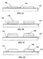
- FIGS. 1A-1 D illustrate a method of manufacturing a single-layer capacitor on metallic foil design.
- FIGS. 1A-1 D illustrate a method of manufacturing a single-layer capacitor on metallic foil design.
- only two capacitors are visible in the sectional views.
- one, two, three, or more capacitors can be formed on a foil by the methods described in this disclosure.
- the following written description is addressed to the formation of only one of the illustrated capacitors for the sake of simplicity.
- metallic foil 110 is provided.
- Metallic foil 110 may be of a type generally available in the industry, for example, copper, copper-invar-copper, invar, nickel, nickel-coated copper, or other metals and alloys having melting points that exceed the firing temperature for thick film pastes. Suitable foils include foils comprised predominantly of copper, such as reverse treated copper foils, double-treated copper foils, and other copper foils commonly used in the multilayer printed circuit board industry.
- the thickness of metallic foil 110 may be in the range of, for example, about 1-100 ⁇ m. Other thickness ranges include 3-75 ⁇ m, and more specifically 12-36 ⁇ m. These thickness ranges correspond to between about 1/3 oz. and 1 oz. copper foil.
- Foil 110 may be pretreated by applying underprint 112 to foil 110.
- Underprint 112 is shown as a surface coating in FIG. 1A, and may be a relatively thin layer applied to the component-side surface of the foil 110.
- Underprint 112 is selected to adhere well to metal foil 110 and to layers subsequently deposited over underprint 112.
- Underprint 112 may be formed, for example, from a paste applied to foil 110 that is fired at a temperature below the melting point of foil 110.
- the underprint paste may be printed as an open coating over the entire surface of foil 110, or printed over selected areas of foil 110. It is generally more economical to print the underprint paste over selected areas of foil 110 rather than over the entire foil 110. However, it may be desirable to coat the entire surface of foil 110 if oxygen-doped firing is used in conjunction with copper foil 110, because glass content in the underprint retards oxidative corrosion of copper foil 110.
- One exemplary paste suitable for use as underprint 112 has the following composition (amounts relative by mass): Copper powder 58.4 Glass A 1.7 Cuprous oxide powder 5.8 Vehicle 11.7 TEXANOL® solvent 12.9 Surfactant 0.5 Total 91.0
- a dielectric material is deposited over underprint 112 on foil 110, forming first dielectric material layer 120 (FIG. 1A).
- the capacitor dielectric material may be, for example, a thick-film capacitor paste that is screen-printed onto foil 110.
- First dielectric material layer 120 is then dried.
- second dielectric material layer 125 is then applied, and dried.
- a single layer of capacitor dielectric material may be deposited to an equivalent thickness of the two layers 120, 125 in a single screen printing step.
- One suitable thick-film capacitor material disclosed for use in fired-on-foil embodiments has the following composition (amounts relative by mass): Barium titanate powder 68.55 Lithium fluoride 1.0 Barium fluoride 1.36 Zinc fluoride 0.74 Glass A 10.25 Glass B 1.0 Glass C 1.0 Vehicle 5.9 TEXANOL® solvent 8.7 Oxidizer 1.0 Phosphate wetting agent 0.5 Total 100.00
- Conductive material layer 130 is formed over second dielectric material layer 125, and dried.
- Conductive material layer 130 can be formed by, for example, screen-printing a thick-film metallic paste over second dielectric material layer 125.
- the paste used to form underprint 112 is also suitable for forming conductive material layer 130.
- the surface area of first and second dielectric layers 120, 125, as would be seen in a top plan view (not shown), is larger than the area of conductive material layer 130.
- First dielectric material layer 120, second dielectric material layer 125, and conductive material layer 130 are then co-fired to sinter the resulting structure together.
- the post-fired structure section is shown in front elevation in FIG. 1 D. Firing results in a single dielectric 128 formed from dielectric layers 120 and 125, because the boundary between dielectric layers 120 and 125 is effectively removed during co-firing. Top electrode 132 also results from the co-firing step.
- FIG. 2 is a phase stability diagram for various oxides at various temperatures and partial pressures of oxygen (PO 2 ) taken from "Electronic Ceramics", R. Buchanan, Ed., Chap. 8, Marcel Dekker, New York, 1990. From diagram one may determine the appropriate atmosphere that will allow any oxide or metal to remain stable for a given temperature. For example, the diagram predicts that at 900°C, copper is in equilibrium with its oxide at a partial pressure of oxygen of 10 -8 atm. Many thick-film compositions contain copper oxide. To maintain copper oxide as copper oxide, therefore, an atmosphere greater than a partial pressure of oxygen of 10 -8 atm may be chosen.
- a partial pressure of oxygen of approximately 10 -6 atm (- 1 ppm of oxygen) is generally chosen, as it represents the typical purity of liquid nitrogen.
- This level of oxygen at 900°C would be at first sight oxidizing to copper and would appear to be deleterious.
- the rate of oxidation of copper at these atmospheres is very slow, such that that copper fired at 900°C in an atmosphere of a few parts per million of oxygen is still essentially free of oxidation.
- copper can tolerate much higher levels of oxygen at lower temperatures without serious oxidation.
- FIG. 2 also illustrates stability thermodynamics for carbon.
- Carbon is a component of the capacitor material vehicle system, and is removed during the initial phases of firing in the burnout zones of the furnace. If carbon is not completely removed in the burnout zones, it will create a highly reducing local atmosphere at 900°C that has a partial pressure of oxygen of approximately 10 -18 atm. When in direct contact with the carbon or within its local atmosphere at this temperature, barium titanate would be partially reduced and oxides such as copper oxide and lead oxide would be rapidly reduced to metal. Such reactions would result in very low insulation resistance or shorting of the dielectric. It is therefore important that the total level of oxygen in the nitrogen flow into the burnout zones is sufficient to completely oxidize and remove the organic components of the vehicle system. This amount can be calculated from the amount of paste deposited on the substrate and the throughput of parts through the furnace.
- FIG. 3 is a calculated plot of equilibrium oxygen vacancy defect concentrations (Vo) expected in pure barium titanate fired at 900°C as a function of oxygen partial pressure. The plot was derived from empirical activation energy of oxygen vacancy concentration data disclosed in "Defect Chemistry of Metal Oxide", D.M. Smyth, Chap. 14, Oxford University Press, 2000. According to FIG. 3, firing barium titanate at 900°C in a partial pressure of oxygen of 10 -6 atm should result in a defect density of approximately 8-10 ppm (see point "A" in FIG. 3). Such a defect density would result in a slightly reduced but acceptable insulation resistance.
- an optimum process for firing capacitors made with barium titanate-based dielectrics on copper foil includes utilizing oxygen-doped burnout zones to effectively oxidize and completely remove the organic content of the vehicle system, without seriously oxidizing the copper foil.
- the actual oxygen dopant level required in the burnout zones depends on the weight of the paste deposit, the throughput, and the nitrogen flow into the burnout zone. Calculations can be performed to determine the theoretical amount of oxygen required.
- the oxygen dopant level may be adjusted in the burnout zones so that the oxygen level never falls below 1 ppm in any of the burnout zones when parts are passing through the furnace in a fully loaded situation. This ensures that essentially all organic material from the vehicle system will be removed during this time frame.
- the firing zone is adjusted to have a low oxygen content to maintain low oxidation of the copper without serious reduction of the barium titanate.
- the cooling zone may also have increased oxygen levels so that relatively oxidizing conditions for the barium titanate exist on cooling, but the temperature is sufficiently low that the copper foil does not become seriously oxidized.
- examples 1 through 11 show that optimum firing zone oxygen levels are approximately 3 ppm. In all cases where 3 ppm was used in the firing zone, insulation resistance was above 1 GO. Optimum burnout zone oxygen is approximately 20 ppm and above for this example. It appears that this range can be quite large and can be extended to at least 40 ppm. The optimum amount depends on the amount of paste deposit on the foil and the throughput through the furnace and may be greater than 40 ppm for high deposits and throughputs.
- the cooling zone is similar in that a reasonably wide range of 3 ppm to 18 ppm has very good insulation resistance and low oxidation of the copper when combined with low oxygen in the firing zone, and 20-39 ppm of oxygen in the burnout zone.
- the thick-film pastes may comprise finely divided particles of ceramic, glass, metal or other solids.
- the particles may have a size on the order of 1 ⁇ m or less, and may be dispersed in an "organic vehicle" comprising polymers dissolved in a mixture of dispersing agent and organic solvent.
- the thick-film glass component of a capacitor material is inert with respect to the high K functional phase, and essentially acts to cohesively bond the composite together and to bond the capacitor composite to the substrate.
- only small amounts of glass are used so that the dielectric constant of the high K functional phase is not excessively diluted.
- Lead germanate glass of the composition Pb 5 Ge 3 O 11 is a ferroelectric glass that has a dielectric constant of approximately 150, and is therefore suitable. Modified versions of lead germanate are also suitable. For example, lead may be partially substituted by barium, and the germanium may be partially substituted by silicon, zirconium, and/or titanium.
- the glass component of the capacitor material softens and flows before the peak firing temperature is reached, coalesces, and encapsulates the functional phase forming the fired capacitor composite.
- Pastes used to form the electrode layers may be based on metallic powders of copper, nickel, silver, silver-palladium compositions, or mixtures of these compounds. Copper powder compositions may be preferred in some applications.
- the desired sintering temperature is determined by the metallic substrate melting temperature, the electrode melting temperature, and the chemical and physical characteristics of the dielectric composition.
- one set of sintering conditions suitable for use in the above embodiments is a nitrogen firing process having a 10 minute residence time above 900°C, and a 6 minute residence time at a peak temperature of 930°C.
Landscapes
- Engineering & Computer Science (AREA)
- Power Engineering (AREA)
- Microelectronics & Electronic Packaging (AREA)
- Ceramic Engineering (AREA)
- Chemical & Material Sciences (AREA)
- Manufacturing & Machinery (AREA)
- Inorganic Chemistry (AREA)
- Parts Printed On Printed Circuit Boards (AREA)
- Ceramic Capacitors (AREA)
- Fixed Capacitors And Capacitor Manufacturing Machines (AREA)
- Production Of Multi-Layered Print Wiring Board (AREA)
Applications Claiming Priority (1)
| Application Number | Priority Date | Filing Date | Title |
|---|---|---|---|
| US11/023,815 US20060141225A1 (en) | 2004-12-28 | 2004-12-28 | Oxygen doped firing of barium titanate on copper foil |
Publications (1)
| Publication Number | Publication Date |
|---|---|
| EP1677320A1 true EP1677320A1 (fr) | 2006-07-05 |
Family
ID=36121293
Family Applications (1)
| Application Number | Title | Priority Date | Filing Date |
|---|---|---|---|
| EP05025289A Withdrawn EP1677320A1 (fr) | 2004-12-28 | 2005-11-18 | Fritage de titanate de barium sur feuille de cuivre sous dopage d'oxygène |
Country Status (6)
| Country | Link |
|---|---|
| US (1) | US20060141225A1 (fr) |
| EP (1) | EP1677320A1 (fr) |
| JP (1) | JP2006191110A (fr) |
| KR (1) | KR20060076702A (fr) |
| CN (1) | CN1848320A (fr) |
| TW (1) | TWI295475B (fr) |
Families Citing this family (2)
| Publication number | Priority date | Publication date | Assignee | Title |
|---|---|---|---|---|
| JPWO2015182114A1 (ja) * | 2014-05-30 | 2017-04-20 | パナソニックIpマネジメント株式会社 | 半導体装置、内蔵用キャパシタユニット、半導体実装体と、内蔵用キャパシタユニットの製造方法 |
| WO2016031206A1 (fr) | 2014-08-29 | 2016-03-03 | パナソニックIpマネジメント株式会社 | Dispositif à semi-conducteur, ensemble, et véhicule |
Citations (3)
| Publication number | Priority date | Publication date | Assignee | Title |
|---|---|---|---|---|
| JP2001135546A (ja) * | 1999-11-09 | 2001-05-18 | Tdk Corp | 積層セラミックコンデンサの製造方法 |
| US20030041427A1 (en) * | 2001-08-23 | 2003-03-06 | Koji Hattori | Multilayer ceramic electronic components and methods for manufacturing the same |
| EP1408520A2 (fr) * | 2002-10-11 | 2004-04-14 | E.I. Du Pont De Nemours And Company | Condensateur céramique co-cuite et procédé de production d'un condensateur céramique pour cartes de circuits imprimés |
Family Cites Families (15)
| Publication number | Priority date | Publication date | Assignee | Title |
|---|---|---|---|---|
| US4190854A (en) * | 1978-02-15 | 1980-02-26 | National Semiconductor Corporation | Trim structure for integrated capacitors |
| US4517155A (en) * | 1982-05-18 | 1985-05-14 | Union Carbide Corporation | Copper base metal termination for multilayer ceramic capacitors |
| US4528613A (en) * | 1984-02-24 | 1985-07-09 | Trw Inc. | Ceramic glass material, capacitor made therefrom and method of making the same |
| US5362534A (en) * | 1993-08-23 | 1994-11-08 | Parlex Corporation | Multiple layer printed circuit boards and method of manufacture |
| US5600533A (en) * | 1994-06-23 | 1997-02-04 | Murata Manufacturing Co., Ltd. | Multilayer ceramic capacitor having an anti-reducing agent |
| US6631551B1 (en) * | 1998-06-26 | 2003-10-14 | Delphi Technologies, Inc. | Method of forming integral passive electrical components on organic circuit board substrates |
| US6420740B1 (en) * | 1999-05-24 | 2002-07-16 | Sharp Laboratories Of America, Inc. | Lead germanate ferroelectric structure with multi-layered electrode |
| US6252761B1 (en) * | 1999-09-15 | 2001-06-26 | National Semiconductor Corporation | Embedded multi-layer ceramic capacitor in a low-temperature con-fired ceramic (LTCC) substrate |
| US6317023B1 (en) * | 1999-10-15 | 2001-11-13 | E. I. Du Pont De Nemours And Company | Method to embed passive components |
| EP1265466A3 (fr) * | 2001-06-05 | 2004-07-21 | Dai Nippon Printing Co., Ltd. | Procédé de fabrication d'un panneau à circuit muni d'éléments passifs et panneau à circuit muni d'éléments passifs |
| US6860000B2 (en) * | 2002-02-15 | 2005-03-01 | E.I. Du Pont De Nemours And Company | Method to embed thick film components |
| JPWO2004040604A1 (ja) * | 2002-10-30 | 2006-03-02 | 三井金属鉱業株式会社 | キャパシタ層形成用の誘電体層付銅箔並びにその誘電体層付銅箔を用いたキャパシタ層形成用の銅張積層板及びそのキャパシタ層形成用の誘電体層付銅箔の製造方法 |
| US6910264B2 (en) * | 2003-01-03 | 2005-06-28 | Phoenix Precision Technology Corp. | Method for making a multilayer circuit board having embedded passive components |
| US20040175585A1 (en) * | 2003-03-05 | 2004-09-09 | Qin Zou | Barium strontium titanate containing multilayer structures on metal foils |
| US7100277B2 (en) * | 2004-07-01 | 2006-09-05 | E. I. Du Pont De Nemours And Company | Methods of forming printed circuit boards having embedded thick film capacitors |
-
2004
- 2004-12-28 US US11/023,815 patent/US20060141225A1/en not_active Abandoned
-
2005
- 2005-11-18 EP EP05025289A patent/EP1677320A1/fr not_active Withdrawn
- 2005-12-09 TW TW094143748A patent/TWI295475B/zh not_active IP Right Cessation
- 2005-12-27 CN CNA2005101381529A patent/CN1848320A/zh active Pending
- 2005-12-27 KR KR1020050130331A patent/KR20060076702A/ko active Search and Examination
- 2005-12-28 JP JP2005379769A patent/JP2006191110A/ja active Pending
Patent Citations (3)
| Publication number | Priority date | Publication date | Assignee | Title |
|---|---|---|---|---|
| JP2001135546A (ja) * | 1999-11-09 | 2001-05-18 | Tdk Corp | 積層セラミックコンデンサの製造方法 |
| US20030041427A1 (en) * | 2001-08-23 | 2003-03-06 | Koji Hattori | Multilayer ceramic electronic components and methods for manufacturing the same |
| EP1408520A2 (fr) * | 2002-10-11 | 2004-04-14 | E.I. Du Pont De Nemours And Company | Condensateur céramique co-cuite et procédé de production d'un condensateur céramique pour cartes de circuits imprimés |
Non-Patent Citations (1)
| Title |
|---|
| PATENT ABSTRACTS OF JAPAN vol. 2000, no. 22 9 March 2001 (2001-03-09) * |
Also Published As
| Publication number | Publication date |
|---|---|
| KR20060076702A (ko) | 2006-07-04 |
| US20060141225A1 (en) | 2006-06-29 |
| CN1848320A (zh) | 2006-10-18 |
| JP2006191110A (ja) | 2006-07-20 |
| TWI295475B (en) | 2008-04-01 |
| TW200629311A (en) | 2006-08-16 |
Similar Documents
| Publication | Publication Date | Title |
|---|---|---|
| KR100465140B1 (ko) | 적층 콘덴서 | |
| KR100553635B1 (ko) | 동시 가열되는 세라믹 커패시터 및 인쇄 회로 기판용세라믹 커패시터를 형성하는 방법 | |
| EP0615262B1 (fr) | Composition céramique diélectrique non-réductrice | |
| EP1612818A1 (fr) | Condensateur à film épais, intégration de ceux-ci dans des circuits imprimés, et procédés de fabrication de ces condensateurs et circuits imprimés | |
| KR20050009225A (ko) | 커패시터용 박막 유전체 및 그의 제조 방법 | |
| EP1667206A1 (fr) | Condensateurs à couche épaisse et leur méthodes de fabrication | |
| EP1879202A2 (fr) | Diélectriques à couche mince avec électrodes cofrittées pour condensateurs et procédés de fabrication correspondant | |
| EP1677320A1 (fr) | Fritage de titanate de barium sur feuille de cuivre sous dopage d'oxygène | |
| KR100803499B1 (ko) | 후막 유전성 및 전도성 조성물 | |
| US7688569B2 (en) | Thick-film dielectric and conductive compositions | |
| US5672220A (en) | Method of producing a laminated electronic device | |
| KR100691370B1 (ko) | 박막 캐패시터의 제조방법과 박막 캐패시터 내장형인쇄회로기판 | |
| US7818855B2 (en) | Method of making thin-film capacitors on metal foil using thick top electrodes | |
| US5662755A (en) | Method of making multi-layered ceramic substrates | |
| US11462339B2 (en) | Dielectric film, dielectric element, and electronic circuit board | |
| US20050204864A1 (en) | Thick-film dielectric and conductive compositions | |
| Borland et al. | Embedding ceramic thick-film capacitors into printed wiring boards | |
| JPH0766563A (ja) | 容量内蔵型多層回路基板 | |
| JP2006093484A (ja) | コンデンサ内蔵ガラスセラミック多層配線基板 | |
| JPH08134388A (ja) | 導電性インキ | |
| JPH08279666A (ja) | 導電性ペースト | |
| JPS63254714A (ja) | 積層コンデンサ素子の製造方法 |
Legal Events
| Date | Code | Title | Description |
|---|---|---|---|
| PUAI | Public reference made under article 153(3) epc to a published international application that has entered the european phase |
Free format text: ORIGINAL CODE: 0009012 |
|
| AK | Designated contracting states |
Kind code of ref document: A1 Designated state(s): AT BE BG CH CY CZ DE DK EE ES FI FR GB GR HU IE IS IT LI LT LU LV MC NL PL PT RO SE SI SK TR |
|
| AX | Request for extension of the european patent |
Extension state: AL BA HR MK YU |
|
| 17P | Request for examination filed |
Effective date: 20070104 |
|
| 17Q | First examination report despatched |
Effective date: 20070208 |
|
| AKX | Designation fees paid |
Designated state(s): DE FR GB |
|
| STAA | Information on the status of an ep patent application or granted ep patent |
Free format text: STATUS: THE APPLICATION IS DEEMED TO BE WITHDRAWN |
|
| 18D | Application deemed to be withdrawn |
Effective date: 20090603 |