EP1676355B1 - Integrierte schaltung zur bereitstellung einer stromgeregelten ladungspumpe mit zum kondensator proportionalem strom - Google Patents
Integrierte schaltung zur bereitstellung einer stromgeregelten ladungspumpe mit zum kondensator proportionalem strom Download PDFInfo
- Publication number
- EP1676355B1 EP1676355B1 EP04795682A EP04795682A EP1676355B1 EP 1676355 B1 EP1676355 B1 EP 1676355B1 EP 04795682 A EP04795682 A EP 04795682A EP 04795682 A EP04795682 A EP 04795682A EP 1676355 B1 EP1676355 B1 EP 1676355B1
- Authority
- EP
- European Patent Office
- Prior art keywords
- current
- charge pump
- voltage
- output
- model
- Prior art date
- Legal status (The legal status is an assumption and is not a legal conclusion. Google has not performed a legal analysis and makes no representation as to the accuracy of the status listed.)
- Expired - Lifetime
Links
- 230000001105 regulatory effect Effects 0.000 title claims abstract description 27
- 239000003990 capacitor Substances 0.000 claims abstract description 45
- 238000000034 method Methods 0.000 claims description 10
- 230000001276 controlling effect Effects 0.000 claims description 7
- 229910044991 metal oxide Inorganic materials 0.000 claims 3
- 150000004706 metal oxides Chemical class 0.000 claims 3
- 230000005669 field effect Effects 0.000 claims 2
- 239000004065 semiconductor Substances 0.000 claims 2
- 238000012358 sourcing Methods 0.000 claims 2
- XUIMIQQOPSSXEZ-UHFFFAOYSA-N Silicon Chemical compound [Si] XUIMIQQOPSSXEZ-UHFFFAOYSA-N 0.000 claims 1
- 230000000295 complement effect Effects 0.000 claims 1
- 229910052710 silicon Inorganic materials 0.000 claims 1
- 239000010703 silicon Substances 0.000 claims 1
- 238000010586 diagram Methods 0.000 description 6
- WHXSMMKQMYFTQS-UHFFFAOYSA-N Lithium Chemical compound [Li] WHXSMMKQMYFTQS-UHFFFAOYSA-N 0.000 description 3
- 230000033228 biological regulation Effects 0.000 description 3
- 229910052744 lithium Inorganic materials 0.000 description 3
- 101710129448 Glucose-6-phosphate isomerase 2 Proteins 0.000 description 1
- 238000010276 construction Methods 0.000 description 1
- 230000009977 dual effect Effects 0.000 description 1
- 238000005516 engineering process Methods 0.000 description 1
- 230000009123 feedback regulation Effects 0.000 description 1
- 238000004519 manufacturing process Methods 0.000 description 1
Images


Classifications
-
- H—ELECTRICITY
- H02—GENERATION; CONVERSION OR DISTRIBUTION OF ELECTRIC POWER
- H02M—APPARATUS FOR CONVERSION BETWEEN AC AND AC, BETWEEN AC AND DC, OR BETWEEN DC AND DC, AND FOR USE WITH MAINS OR SIMILAR POWER SUPPLY SYSTEMS; CONVERSION OF DC OR AC INPUT POWER INTO SURGE OUTPUT POWER; CONTROL OR REGULATION THEREOF
- H02M3/00—Conversion of DC power input into DC power output
- H02M3/02—Conversion of DC power input into DC power output without intermediate conversion into AC
- H02M3/04—Conversion of DC power input into DC power output without intermediate conversion into AC by static converters
- H02M3/06—Conversion of DC power input into DC power output without intermediate conversion into AC by static converters using resistors or capacitors, e.g. potential divider
- H02M3/07—Conversion of DC power input into DC power output without intermediate conversion into AC by static converters using resistors or capacitors, e.g. potential divider using capacitors charged and discharged alternately by semiconductor devices with control electrode, e.g. charge pumps
- H02M3/073—Charge pumps of the Schenkel-type
-
- H—ELECTRICITY
- H02—GENERATION; CONVERSION OR DISTRIBUTION OF ELECTRIC POWER
- H02M—APPARATUS FOR CONVERSION BETWEEN AC AND AC, BETWEEN AC AND DC, OR BETWEEN DC AND DC, AND FOR USE WITH MAINS OR SIMILAR POWER SUPPLY SYSTEMS; CONVERSION OF DC OR AC INPUT POWER INTO SURGE OUTPUT POWER; CONTROL OR REGULATION THEREOF
- H02M3/00—Conversion of DC power input into DC power output
- H02M3/02—Conversion of DC power input into DC power output without intermediate conversion into AC
- H02M3/04—Conversion of DC power input into DC power output without intermediate conversion into AC by static converters
- H02M3/06—Conversion of DC power input into DC power output without intermediate conversion into AC by static converters using resistors or capacitors, e.g. potential divider
- H02M3/07—Conversion of DC power input into DC power output without intermediate conversion into AC by static converters using resistors or capacitors, e.g. potential divider using capacitors charged and discharged alternately by semiconductor devices with control electrode, e.g. charge pumps
-
- H—ELECTRICITY
- H02—GENERATION; CONVERSION OR DISTRIBUTION OF ELECTRIC POWER
- H02M—APPARATUS FOR CONVERSION BETWEEN AC AND AC, BETWEEN AC AND DC, OR BETWEEN DC AND DC, AND FOR USE WITH MAINS OR SIMILAR POWER SUPPLY SYSTEMS; CONVERSION OF DC OR AC INPUT POWER INTO SURGE OUTPUT POWER; CONTROL OR REGULATION THEREOF
- H02M1/00—Details of apparatus for conversion
- H02M1/0045—Converters combining the concepts of switch-mode regulation and linear regulation, e.g. linear pre-regulator to switching converter, linear and switching converter in parallel, same converter or same transistor operating either in linear or switching mode
Definitions
- Battery operated appliances have proliferated throughout the world.
- Cell phone handsets, portable radios and playback units, personal digital assistants, light emitting diode (LED) flashlights, and wireless security and remote control systems provide only a few of many examples of such appliances.
- Small batteries of the types commonly employed in these appliances typically do not put out either constant current or constant voltage.
- feedback regulation techniques are employed in order for output loads, such as LEDs to be supplied with constant current. Regulation may be as simple as a ballast resistor or as complex as an integrated circuit with feedback control.
- LEDs typically require a supply voltage potential which frequently exceeds the voltage potential supplied by a particular cell or low voltage battery.
- white LEDs have a forward voltage of 3.5 volts typical, and 4.0 volts maximum, at a current of 20 milliamperes (mA), whereas a single-cell lithium battery delivers approximately 3.6 volts and two alkaline cells in series deliver approximately 3.0 volts.
- a voltage converter is typically employed to boost the voltage to a level suitable for supplying the LED.
- a charge pump circuit topology Another known way to generate constant current for a load, such as an LED, is to employ a charge pump circuit topology.
- a type MAX684 voltage regulated charge pump supplied by Maxim Integrated Products, Inc., Sunnyvale, California, can power three or more white color LEDs.
- the MAX684 charge pump regulator generates 5 volts from a 2.7V to 4.2V input, but requires a ballast resistor or current source for each LED as well as external capacitors.
- the ballast resistors lower the efficiency of the driver by the large voltage drop needed.
- Maxim suggests that an external switching transistor controlled by a PWM brightness control be employed.
- a charge pump circuit which is configured for suitably controlling the charging current in the charge pump capacitors.
- the charge pump circuit comprises an input current controlling circuit comprising a current limiting device for controlling the inrush current, and thus the charging current in the charge pump capacitors.
- the input current controlling circuit is configured to regulate the average voltage at the output of the current limiting device to correspond to the average voltage at the output of a pass device configured for regulating the output current. Accordingly, the total input current, and thus the charging current in the charge pump capacitors, can be suitably controlled at all times to significantly reduce the impact of any instantaneous charging currents.
- a hitherto unsolved need has arisen to provide a single, integrated circuit driver which uses a charge pump topology in which magnitude of output current to a load is adjusted by the scaling of capacitance of a single external flying capacitor and maintained at the scaled level, in a manner overcoming limitations and drawbacks of the prior art.
- Still one more object of the present invention is to provide a low-cost, high frequency charge pump integrated circuit for driving one to four super-bright LEDs, for example, with a constant current over an input voltage range usually present with battery power supplies and without need for any external current sense resistor.
- Yet one more object of the present invention is to provide a low-cost six-pin current regulated charge pump driver IC with external enable and user settable regulated drive current, which can be fabricated using known low-cost CMOS IC processes.
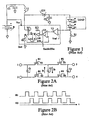
- the primary charge pump 12 utilizes the externally connected capacitor Cp as its flying capacitor, whereas the model charge pump 14 utilizes an internal capacitor Cm formed on the integrated circuit chip as its flying capacitor.
- the primary charge pump 12 has an output V1 that forms the OUT path for the IC 10.
- the model charge pump 14 has an output V2.
- a voltage amplifier U3 (having finite gain) subtracts the V2 output from the V1 output to provide a difference voltage.
- the circuit U3 may be implemented in a variety of manners including, but not limited to, an operational amplifier or a PMOS differential pair. The difference voltage put out by U3 is applied to a control gate electrode of a PMOS transistor M2.
- a series pass regulator element represented in the Figure 3 block diagram as a PMOS transistor M3, is provided to adjust the input drive level from a DC supply 18, such as a lithium battery, to the primary charge pump 12 and the model charge pump 14.
- An input capacitor C3 minimizes voltage drops at the input of the IC 10 in response to high frequency switching operations occurring within the charge pumps 12 and 14.
- An output capacitor C4 acts to filter out any switching transients otherwise remaining in the output current supplied by IC 10.
- a current controlled voltage source U4 has an input connected to a node between the drain electrode of PMOS transistor M2 and the constant current source 16, and has an output connected to a gate control electrode of the pass element PMOS transistor M3.
- the circuit U4 functions as a current-to-voltage converter and generates a voltage control as a function of current imbalance between Imodel and Iref sensed at its input.
- the voltage control is applied to a control gate electrode of the pass element M3 such that the current Imodel passing through the PMOS transistor M2 is forced to remain equal to the internal fixed reference current Iref generated by constant current source 16. If Imodel is greater than Iref, excess current present at the input of U4 is sinked to ground through U4 and the voltage control to M3 causes input current to be reduced. If Imodel is less than Iref, additional current is sourced by U4 to the constant current source 16 and the voltage control to M3 causes input current to the charge pumps to be increased. This regulation process operates automatically to maintain Imodel equal to Iref.
- the integrated circuit 10 includes an internal clock element 20 which generates the non-overlapping switching signals Phi 1 (i.e. ⁇ 1) and Phi 2 (i.e. ⁇ 2) shown in Figure 2B at a suitable clock frequency, such as 1.2 MHz for example, and applies them simultaneously to control the primary charge pump 12 and the model charge pump 14.
- a true logical level at the enable pin EN of IC 10 enables the circuitry to generate and put out regulated current Iout to a load 22.
- the load may be any desired load, particularly but not necessarily one or more super-bright LEDs.
- a low frequency pulse width modulator (PWM) signal applied to the enable pin EN turns the IC 10 on and off, thereby modulating the output current and dimming the LED light level, for example. For example, applying a 1 KHz PWM signal with a duty cycle of 700 microseconds results in a light level which is 70% of the maximum drive level set by the external switched capacitor Cp.
- PWM pulse width modulator
- a 100 nanofarad (nF) capacitor Cp results in approximately 30 mA of output current
- a 47 nF capacitor Cp results in approximately 20 mA of output current
- a 22 nF capacitor results in approximately 15 mA of output current
- a 10 nF capacitor results in approximately 5 mA of output current, from IC 10.
- a switching frequency of 1.2 MHz full current is reached in approximately four microseconds from first assertion of the enable signal.
- the present invention provides a charge pump based driver integrated circuit 10 providing constant current regulation, user settable by selection of an external flying capacitance value, with a wide current range extending to 100 mA, or more.
- the circuit 10 operates with a wide input voltage range, for example 1.6 volts to 5.0 volts. When non-enabled in shutdown mode, the circuit 10 draws as little as 2 ⁇ A.
- the circuit 10 enable may be pulse width modulated so as to provide a ten to one linear dimming range for LEDs.
- Applications for the integrated circuit 10 include, but are clearly not limited to, driving super-bright LED flashlights, battery-powered indicator lights, cell phone display panel back lighting, keyless entry systems, wireless security systems, automatic meter readers, etc.
Landscapes
- Engineering & Computer Science (AREA)
- Power Engineering (AREA)
- Dc-Dc Converters (AREA)
- Stabilization Of Oscillater, Synchronisation, Frequency Synthesizers (AREA)
Claims (12)
- Elektrisches System (10) zum Einstellen von elektrischem Strom, der von einer Stromquelle (18) zu einer Last (22) fließt, wobei das elektrische System umfasst:a) ein Stromdurchgangsreglerelement (M3), das an die Stromquelle derart anschließbar ist, dass es einen von der Stromquelle bezogenen Zufuhrstrom durch eine Steuerspannung (V0) steuert,b) eine Primär-Ladungspumpe (12) aufweisend einen an das Stromdurchgangsreglerelement angeschlossenen Eingang und einen an die Last anschließbaren Ausgang, Pin-Anschlüsse an einen externen Flying-Kondensator (Cp), der einen Benutzer gewählten Kapazitätswert aufweist, um den eingestellten Ausgangsstrompegel festzulegen, der zur Last fließt,c) eine Modell-Ladungspumpe (14), die einen an das Stromdurchgangsreglerelement angeschlossenen Eingang und einen eine Ausgangsspannung (V2) liefernden Ausgang enthält,d) eine Stromerfassungsschaltung (U3, M2), die derart angeschlossen ist, dass sie die Ausgangsspannung von der Modell-Ladungspumpe vorgibt, um mit einer Ausgangsspannung (V1) von der Primär-Ladungspumpe gleich zu sein, und die einen Modellstrom Imodel basierend auf der Differenz zwischen den Ausgangsspannungen der Modell-Ladungspumpe und der Primär-Ladungspumpe liefert,e) eine Konstantstromquelle (16) zum Ziehen eines Referenzstromes Iref, undf) eine Steuerschaltung (U4), die auf die Stromerfassungsschaltung und die Konstantstromquelle reagiert und die derart angeschlossen ist, dass sie das Stromdurchgangsreglerelement durch die Steuerspannung (V0) derart steuert, dass es den Modellstrom Imodel vorgibt, um mit dem Referenzstrom Iref gleich zu sein, so dass der durch die Primär-Ladungspumpe durchströmende Strom auf einen durch den Flying-Kondensator festgelegten Pegel eingestellt ist, der unabhängig von einer Eingangsspannungsveränderung der Stromquelle ist.
- Elektrisches System nach Anspruch 1, welches einen nicht-überlappenden Zwei-Phasen-Takt-Erzeuger (20) enthält, und wobei die Primär-Ladungspumpe durch den Takt-Erzeuger getaktet ist.
- Elektrisches System nach Anspruch 2, wobei die Modell-Ladungspumpe in Synchronität mit der Primär-Ladungspumpe getaktet ist.
- Elektrisches System nach Anspruch 3, wobei die Stromerfassungsschaltung eine Spannungsvergleichsschaltung (43), die einen ersten Eingang aufweist, der derart angeschlossen ist, dass er die Ausgangsspannung der Primär-Ladungspumpe überwacht, die einen zweiten Eingang aufweist, der derart angeschlossen ist, dass er die Ausgangsspannung der Modell-Ladungspumpe überwacht, und die einen Spannungsvergleichsausgang aufweist, und einen Modellstrom-Regler (M2) umfasst, der auf den Spannungsvergleichsausgang reagiert und der derart angeschlossen ist, dass er die Ausgangsspannung der Modell-Ladungspumpe vorgibt, um mit der Ausgangsspannung der Primär-Ladungspumpe gleich zu sein.
- Elektrisches System nach Anspruch 4, wobei der Modellstrom-Regler der Stromerfassungsschaltung in Serie mit der Konstantstromquelle angeschlossen ist und wobei die Steuerschaltung eine stromgesteuerte Quelle umfasst, die einen Eingangsanschluss an einen Knoten zwischen dem Modellstrom-Regler und der Konstantstromquelle zum Beziehen und Ziehen von Strom aufweist, um den Modellstrom Imodel mit dem Referenzstrom Iref gleich zu halten, und die einen Ausgang aufweist, der derart angeschlossen ist, dass er den durch das Stromdurchgangsreglerelement durchströmenden Strom steuert, wobei das Stromdurchgangsreglerelement einen spannungsgesteuerten Stromerzeuger umfasst und wobei die stromgesteuerte Quelle eine stromgesteuerte Spannungsquelle zum Ausgeben der Steuerspannung (V0) umfasst.
- Elektrisches System nach Anspruch 4, wobei der Modellstrom-Regler einen Metall-Oxid-Halbleiter-Feldeffekt-Transistor umfasst, wobei der spannungsgesteuerte Stromregler einen Metallregler-Oxid-Halbleiter-Feldeffekt-Transistor umfasst.
- Elektrisches System nach Anspruch 1, welches als ein monolitischintegrierter Schaltungschip ohne den Flying-Kondensator und aufweisend die externen Anschlüsse an die Stromquelle, die Last und den Flying-Kondensator gebildet ist, und wobei das elektrische System einen zusätzlichen externen Anschluss an ein Aktivierungssignal aufweist.
- Elektrisches System nach Anspruch 7, welches in einer Sechs-Pinintegrierten Schaltungsbaugruppe enthalten ist, welche einen Stromquellen-Pin, einen Masserückführungs-Pin, einen Last-Pin, einen Aktivierungs-Pin und zwei Pins zum Anschließen des Flying-Kondensators umfasst, wobei die Baugruppe mit einer Industriestandard-SOT-23-Baugruppenkonvention konform ist.
- Elektrisches System nach Anspruch 1, wobei die Stromquelle eine Batterie umfasst und die Last wenigstens eine Licht emittierende Diode umfasst.
- Elektrisches System nach einem der vorhergehenden Ansprüche, wobei die Primär-Ladungspumpe die gleiche Schaltungstopologie wie die Modell-Ladungspumpe aufWeist und elektrisch proportional zur Modell-Ladungspumpe ist.
- Integrierte Schaltung, die in Übereinstimmung mit einem komplementären Metall-Oxid-Silizium-VerFahren zum Einstellen von elektrischem Strom gebildet ist, der von einer Batterie-Stromquelle zu einer Last fließt, ohne dass ein externer Stromerfassungswiderstand erforderlich ist, wobei die integrierte Schaltung das elektrische System gemäß Anspruch 1 umfasst,
wobei die Stromerfassungsschaltung derart angeschlossen und wirksam ist, dass sie Spannungspegel an den Ausgängen der Primär- und der Modell-Ladungspumpe vergleicht und Spannungspegel am Ausgang der Modell-Ladungspumpe vorgibt, um mit einem Spannungspegel am Ausgang der Primär-Ladungspumpe gleich zu sein, und
wobei die Steuerschaltung einen Strom beziehenden/ziehenden Eingang aufweist, der an einen Knoten zwischen der Stromerfassungsschaltung und der Konstantstromquelle verbunden ist und der einen Steuerausgang aufweist, welcher derart angeschlossen ist, dass er das Stromdurchgangsreglerelement derart steuert, dass es den Strom Imodel vorgibt, um mit dem Referenzstrom Iref gleich zu sein, so dass der durch die Primär-Ladungspumpe durchströmende Strom auf einen durch den Kapazitätswert des Flying-Kondensators festgelegten Pegel eingestellt ist, der unabhängig von Spannungsveränderungen der Batterie-Stromquelle ist. - Verfahren zum Einstellen von Strom, der von einer Batterie zu einer Last fließt, ohne den Stromfluss zur Last direkt zu erfassen, umfassend die Schritte:a) Durchströmen von Strom von der Batterie durch ein Stromdurchgangsreglerelement, das durch eine Steuerspannung VO bestimmt wird,b) Bereitstellen von Strom vom Stromdurchgangsreglerelement an eine Primär-Ladungspumpe, die einen eingestellten Stromfluss an die Last bereitstellt,c) Auswählen eines Wertes für einen Flying-Kondensator Cp, der einen Benutzer gewählten Kapazitätswert der Primär-Ladungspumpe dazu aufweist, einen eingestellten Ausgangsstrompegel festzulegen, der zur Last fließt,d) Bereitstellen von Strom vom Stromdurchgangsreglerelement an eine Modell-Ladungspumpe, um eine Ausgangsspannung V2 zu erzeugen,e) Durchströmen der Ausgangsspannung V2 zu einer Stromerfassungsschaltung, um einen Modellstrom Imodel basierend auf der Differenz zwischen den Ausgangsspannungen von der Modell-Ladungspumpe und der Primär-Ladungspumpe zu liefern, und Durchströmen des Modellstromes Imodel in eine Konstantstromquelle zum Ziehen eines Referenzstromes Iref,f) Steuern der Stromerfassungsschaltung, um einen Spannungspegel am Ausgang der Modell-Ladungspumpe vorzugeben, mit einem Spannungspegel am Ausgang der Primär-Ladungspumpe gleich zu sein, undg) Steuern des Stromdurchgangsreglerelementes durch die Steuerspannung, um den Strom Imodel vorzugeben, mit dem Referenzstrom Iref gleich zu sein, so dass der durch die Primär-Ladungspumpe durchströmende Strom auf einen durch den Flying-Kondensator festgelegten Pegel eingestellt wird, der unabhängig von Eingangspannungsveränderungen der Stromquelle ist.
Applications Claiming Priority (2)
| Application Number | Priority Date | Filing Date | Title |
|---|---|---|---|
| US10/689,183 US6873203B1 (en) | 2003-10-20 | 2003-10-20 | Integrated device providing current-regulated charge pump driver with capacitor-proportional current |
| PCT/US2004/034549 WO2005043734A1 (en) | 2003-10-20 | 2004-10-19 | Integrated device providing current-regulated charge pump driver with capacitor-proportional current |
Publications (2)
| Publication Number | Publication Date |
|---|---|
| EP1676355A1 EP1676355A1 (de) | 2006-07-05 |
| EP1676355B1 true EP1676355B1 (de) | 2010-06-16 |
Family
ID=34314183
Family Applications (1)
| Application Number | Title | Priority Date | Filing Date |
|---|---|---|---|
| EP04795682A Expired - Lifetime EP1676355B1 (de) | 2003-10-20 | 2004-10-19 | Integrierte schaltung zur bereitstellung einer stromgeregelten ladungspumpe mit zum kondensator proportionalem strom |
Country Status (8)
| Country | Link |
|---|---|
| US (1) | US6873203B1 (de) |
| EP (1) | EP1676355B1 (de) |
| JP (1) | JP4515457B2 (de) |
| KR (1) | KR101191701B1 (de) |
| CN (1) | CN100505489C (de) |
| AT (1) | ATE471592T1 (de) |
| DE (1) | DE602004027749D1 (de) |
| WO (1) | WO2005043734A1 (de) |
Cited By (1)
| Publication number | Priority date | Publication date | Assignee | Title |
|---|---|---|---|---|
| US11972807B2 (en) | 2022-05-11 | 2024-04-30 | Sandisk Technologies Llc | Charge pump current regulation during voltage ramp |
Families Citing this family (130)
| Publication number | Priority date | Publication date | Assignee | Title |
|---|---|---|---|---|
| US8149048B1 (en) | 2000-10-26 | 2012-04-03 | Cypress Semiconductor Corporation | Apparatus and method for programmable power management in a programmable analog circuit block |
| US7765095B1 (en) | 2000-10-26 | 2010-07-27 | Cypress Semiconductor Corporation | Conditional branching in an in-circuit emulation system |
| US8103496B1 (en) | 2000-10-26 | 2012-01-24 | Cypress Semicondutor Corporation | Breakpoint control in an in-circuit emulation system |
| US6724220B1 (en) | 2000-10-26 | 2004-04-20 | Cyress Semiconductor Corporation | Programmable microcontroller architecture (mixed analog/digital) |
| US8176296B2 (en) | 2000-10-26 | 2012-05-08 | Cypress Semiconductor Corporation | Programmable microcontroller architecture |
| US8160864B1 (en) | 2000-10-26 | 2012-04-17 | Cypress Semiconductor Corporation | In-circuit emulator and pod synchronized boot |
| US7406674B1 (en) | 2001-10-24 | 2008-07-29 | Cypress Semiconductor Corporation | Method and apparatus for generating microcontroller configuration information |
| JP3608199B2 (ja) * | 2001-10-30 | 2005-01-05 | ローム株式会社 | Ic間のインターフェースシステム、及びic |
| US8078970B1 (en) | 2001-11-09 | 2011-12-13 | Cypress Semiconductor Corporation | Graphical user interface with user-selectable list-box |
| US8042093B1 (en) | 2001-11-15 | 2011-10-18 | Cypress Semiconductor Corporation | System providing automatic source code generation for personalization and parameterization of user modules |
| US7770113B1 (en) | 2001-11-19 | 2010-08-03 | Cypress Semiconductor Corporation | System and method for dynamically generating a configuration datasheet |
| US8069405B1 (en) | 2001-11-19 | 2011-11-29 | Cypress Semiconductor Corporation | User interface for efficiently browsing an electronic document using data-driven tabs |
| US6971004B1 (en) | 2001-11-19 | 2005-11-29 | Cypress Semiconductor Corp. | System and method of dynamically reconfiguring a programmable integrated circuit |
| US7774190B1 (en) | 2001-11-19 | 2010-08-10 | Cypress Semiconductor Corporation | Sleep and stall in an in-circuit emulation system |
| US7844437B1 (en) | 2001-11-19 | 2010-11-30 | Cypress Semiconductor Corporation | System and method for performing next placements and pruning of disallowed placements for programming an integrated circuit |
| US8103497B1 (en) | 2002-03-28 | 2012-01-24 | Cypress Semiconductor Corporation | External interface for event architecture |
| US7308608B1 (en) | 2002-05-01 | 2007-12-11 | Cypress Semiconductor Corporation | Reconfigurable testing system and method |
| US7761845B1 (en) | 2002-09-09 | 2010-07-20 | Cypress Semiconductor Corporation | Method for parameterizing a user module |
| US7151433B2 (en) * | 2003-08-05 | 2006-12-19 | Chun James K | Combination LED flashlight and garage door transmitter |
| US7295049B1 (en) | 2004-03-25 | 2007-11-13 | Cypress Semiconductor Corporation | Method and circuit for rapid alignment of signals |
| US7408527B2 (en) * | 2004-04-30 | 2008-08-05 | Infocus Corporation | Light emitting device driving method and projection apparatus so equipped |
| US20050259453A1 (en) * | 2004-05-21 | 2005-11-24 | Weng Da F | Switching capacitor network auxiliary voltage source for off-line IC chip |
| US8286125B2 (en) | 2004-08-13 | 2012-10-09 | Cypress Semiconductor Corporation | Model for a hardware device-independent method of defining embedded firmware for programmable systems |
| US8069436B2 (en) | 2004-08-13 | 2011-11-29 | Cypress Semiconductor Corporation | Providing hardware independence to automate code generation of processing device firmware |
| US7332976B1 (en) | 2005-02-04 | 2008-02-19 | Cypress Semiconductor Corporation | Poly-phase frequency synthesis oscillator |
| US8618866B2 (en) * | 2005-04-29 | 2013-12-31 | Ati Technologies Ulc | Apparatus and methods for balancing supply voltages |
| US7400183B1 (en) | 2005-05-05 | 2008-07-15 | Cypress Semiconductor Corporation | Voltage controlled oscillator delay cell and method |
| TWI310292B (en) * | 2005-06-14 | 2009-05-21 | Richtek Technology Corp | Dimming method and system thereof |
| US8089461B2 (en) | 2005-06-23 | 2012-01-03 | Cypress Semiconductor Corporation | Touch wake for electronic devices |
| US7307485B1 (en) | 2005-11-14 | 2007-12-11 | Cypress Semiconductor Corporation | Capacitance sensor using relaxation oscillators |
| GB2436619B (en) * | 2005-12-19 | 2010-10-06 | Toumaz Technology Ltd | Sensor circuits |
| US8085067B1 (en) | 2005-12-21 | 2011-12-27 | Cypress Semiconductor Corporation | Differential-to-single ended signal converter circuit and method |
| WO2007084115A1 (en) * | 2006-01-17 | 2007-07-26 | Semiconductor Components Industries, L.L.C. | Regulated charge pump and method therefor |
| US7312616B2 (en) | 2006-01-20 | 2007-12-25 | Cypress Semiconductor Corporation | Successive approximate capacitance measurement circuit |
| US20070177412A1 (en) * | 2006-01-31 | 2007-08-02 | Power-One, Inc. | Charge pumped driver for switched mode power supply |
| US20070176903A1 (en) * | 2006-01-31 | 2007-08-02 | Dahlin Jeffrey J | Capacitive touch sensor button activation |
| US7279958B1 (en) * | 2006-02-27 | 2007-10-09 | National Semiconductor Corporation | Synthesized resonation for an EL driver circuit |
| US7439679B2 (en) * | 2006-03-16 | 2008-10-21 | Motorola, Inc. | Method and apparatus for illuminating light sources within an electronic device |
| US8067948B2 (en) | 2006-03-27 | 2011-11-29 | Cypress Semiconductor Corporation | Input/output multiplexer bus |
| US8144125B2 (en) | 2006-03-30 | 2012-03-27 | Cypress Semiconductor Corporation | Apparatus and method for reducing average scan rate to detect a conductive object on a sensing device |
| US8040142B1 (en) | 2006-03-31 | 2011-10-18 | Cypress Semiconductor Corporation | Touch detection techniques for capacitive touch sense systems |
| US7721609B2 (en) | 2006-03-31 | 2010-05-25 | Cypress Semiconductor Corporation | Method and apparatus for sensing the force with which a button is pressed |
| ITMI20060758A1 (it) * | 2006-04-14 | 2007-10-15 | Atmel Corp | Metodo e circuito per l'alimentazione di tensione per circuiteria di orologio a tempo reale basata su una pompa di carica a tensione regolata |
| US7723926B2 (en) * | 2006-05-15 | 2010-05-25 | Supertex, Inc. | Shunting type PWM dimming circuit for individually controlling brightness of series connected LEDS operated at constant current and method therefor |
| US8089472B2 (en) | 2006-05-26 | 2012-01-03 | Cypress Semiconductor Corporation | Bidirectional slider with delete function |
| US8537121B2 (en) * | 2006-05-26 | 2013-09-17 | Cypress Semiconductor Corporation | Multi-function slider in touchpad |
| CN101449452B (zh) * | 2006-07-07 | 2012-06-27 | 半导体元件工业有限责任公司 | 恒定电流电荷泵控制器 |
| US8040321B2 (en) | 2006-07-10 | 2011-10-18 | Cypress Semiconductor Corporation | Touch-sensor with shared capacitive sensors |
| US7253643B1 (en) | 2006-07-19 | 2007-08-07 | Cypress Semiconductor Corporation | Uninterrupted radial capacitive sense interface |
| US9507465B2 (en) * | 2006-07-25 | 2016-11-29 | Cypress Semiconductor Corporation | Technique for increasing the sensitivity of capacitive sensor arrays |
| US9766738B1 (en) | 2006-08-23 | 2017-09-19 | Cypress Semiconductor Corporation | Position and usage based prioritization for capacitance sense interface |
| US8547114B2 (en) | 2006-11-14 | 2013-10-01 | Cypress Semiconductor Corporation | Capacitance to code converter with sigma-delta modulator |
| US8089288B1 (en) | 2006-11-16 | 2012-01-03 | Cypress Semiconductor Corporation | Charge accumulation capacitance sensor with linear transfer characteristic |
| US8058937B2 (en) | 2007-01-30 | 2011-11-15 | Cypress Semiconductor Corporation | Setting a discharge rate and a charge rate of a relaxation oscillator circuit |
| US8026739B2 (en) | 2007-04-17 | 2011-09-27 | Cypress Semiconductor Corporation | System level interconnect with programmable switching |
| US8040266B2 (en) | 2007-04-17 | 2011-10-18 | Cypress Semiconductor Corporation | Programmable sigma-delta analog-to-digital converter |
| US9564902B2 (en) | 2007-04-17 | 2017-02-07 | Cypress Semiconductor Corporation | Dynamically configurable and re-configurable data path |
| US8516025B2 (en) | 2007-04-17 | 2013-08-20 | Cypress Semiconductor Corporation | Clock driven dynamic datapath chaining |
| US8130025B2 (en) | 2007-04-17 | 2012-03-06 | Cypress Semiconductor Corporation | Numerical band gap |
| US8092083B2 (en) | 2007-04-17 | 2012-01-10 | Cypress Semiconductor Corporation | Temperature sensor with digital bandgap |
| US7737724B2 (en) | 2007-04-17 | 2010-06-15 | Cypress Semiconductor Corporation | Universal digital block interconnection and channel routing |
| US8266575B1 (en) | 2007-04-25 | 2012-09-11 | Cypress Semiconductor Corporation | Systems and methods for dynamically reconfiguring a programmable system on a chip |
| US9720805B1 (en) | 2007-04-25 | 2017-08-01 | Cypress Semiconductor Corporation | System and method for controlling a target device |
| US8065653B1 (en) | 2007-04-25 | 2011-11-22 | Cypress Semiconductor Corporation | Configuration of programmable IC design elements |
| US8144126B2 (en) | 2007-05-07 | 2012-03-27 | Cypress Semiconductor Corporation | Reducing sleep current in a capacitance sensing system |
| JP4912229B2 (ja) * | 2007-06-18 | 2012-04-11 | 株式会社リコー | 負荷駆動回路及びその負荷電流設定方法 |
| US9500686B1 (en) | 2007-06-29 | 2016-11-22 | Cypress Semiconductor Corporation | Capacitance measurement system and methods |
| WO2009006556A1 (en) | 2007-07-03 | 2009-01-08 | Cypress Semiconductor Corporation | Normalizing capacitive sensor array signals |
| US8089289B1 (en) | 2007-07-03 | 2012-01-03 | Cypress Semiconductor Corporation | Capacitive field sensor with sigma-delta modulator |
| US8570053B1 (en) | 2007-07-03 | 2013-10-29 | Cypress Semiconductor Corporation | Capacitive field sensor with sigma-delta modulator |
| US8169238B1 (en) * | 2007-07-03 | 2012-05-01 | Cypress Semiconductor Corporation | Capacitance to frequency converter |
| US8049569B1 (en) | 2007-09-05 | 2011-11-01 | Cypress Semiconductor Corporation | Circuit and method for improving the accuracy of a crystal-less oscillator having dual-frequency modes |
| KR100944956B1 (ko) * | 2007-11-19 | 2010-03-02 | (주)프로차일드 | 지그비 모뎀을 이용한 조명등 원격 제어 회로 |
| US8723807B2 (en) * | 2008-01-09 | 2014-05-13 | Integrated Device Technology, Inc. | Combined touch sensor and LED driver with n-type MOSFET protecting touch sensor |
| US8040070B2 (en) | 2008-01-23 | 2011-10-18 | Cree, Inc. | Frequency converted dimming signal generation |
| US8525798B2 (en) | 2008-01-28 | 2013-09-03 | Cypress Semiconductor Corporation | Touch sensing |
| CN102017397B (zh) * | 2008-01-31 | 2015-09-16 | 半导体元件工业有限责任公司 | 电荷泵变换器及其方法 |
| US8487912B1 (en) | 2008-02-01 | 2013-07-16 | Cypress Semiconductor Corporation | Capacitive sense touch device with hysteresis threshold |
| US8319505B1 (en) | 2008-10-24 | 2012-11-27 | Cypress Semiconductor Corporation | Methods and circuits for measuring mutual and self capacitance |
| US8358142B2 (en) | 2008-02-27 | 2013-01-22 | Cypress Semiconductor Corporation | Methods and circuits for measuring mutual and self capacitance |
| US9104273B1 (en) | 2008-02-29 | 2015-08-11 | Cypress Semiconductor Corporation | Multi-touch sensing method |
| US8321174B1 (en) | 2008-09-26 | 2012-11-27 | Cypress Semiconductor Corporation | System and method to measure capacitance of capacitive sensor array |
| TWI397034B (zh) * | 2008-10-29 | 2013-05-21 | Richtek Technology Corp | 改善led顯示系統效能的電流調節器及方法 |
| US8487639B1 (en) | 2008-11-21 | 2013-07-16 | Cypress Semiconductor Corporation | Receive demodulator for capacitive sensing |
| US8866500B2 (en) | 2009-03-26 | 2014-10-21 | Cypress Semiconductor Corporation | Multi-functional capacitance sensing circuit with a current conveyor |
| US9448964B2 (en) | 2009-05-04 | 2016-09-20 | Cypress Semiconductor Corporation | Autonomous control in a programmable system |
| US8217591B2 (en) * | 2009-05-28 | 2012-07-10 | Cree, Inc. | Power source sensing dimming circuits and methods of operating same |
| TWI406592B (zh) * | 2009-07-10 | 2013-08-21 | Richtek Technology Corp | 低接腳數led驅動器積體電路 |
| US8723827B2 (en) | 2009-07-28 | 2014-05-13 | Cypress Semiconductor Corporation | Predictive touch surface scanning |
| US8933665B2 (en) | 2009-08-05 | 2015-01-13 | Apple Inc. | Balancing voltages between battery banks |
| US8901845B2 (en) | 2009-09-24 | 2014-12-02 | Cree, Inc. | Temperature responsive control for lighting apparatus including light emitting devices providing different chromaticities and related methods |
| US10264637B2 (en) | 2009-09-24 | 2019-04-16 | Cree, Inc. | Solid state lighting apparatus with compensation bypass circuits and methods of operation thereof |
| US9713211B2 (en) * | 2009-09-24 | 2017-07-18 | Cree, Inc. | Solid state lighting apparatus with controllable bypass circuits and methods of operation thereof |
| US8777449B2 (en) | 2009-09-25 | 2014-07-15 | Cree, Inc. | Lighting devices comprising solid state light emitters |
| US8602579B2 (en) | 2009-09-25 | 2013-12-10 | Cree, Inc. | Lighting devices including thermally conductive housings and related structures |
| US9285103B2 (en) * | 2009-09-25 | 2016-03-15 | Cree, Inc. | Light engines for lighting devices |
| US9068719B2 (en) | 2009-09-25 | 2015-06-30 | Cree, Inc. | Light engines for lighting devices |
| US9464801B2 (en) | 2009-09-25 | 2016-10-11 | Cree, Inc. | Lighting device with one or more removable heat sink elements |
| US9353933B2 (en) * | 2009-09-25 | 2016-05-31 | Cree, Inc. | Lighting device with position-retaining element |
| US9217542B2 (en) | 2009-10-20 | 2015-12-22 | Cree, Inc. | Heat sinks and lamp incorporating same |
| US9030120B2 (en) * | 2009-10-20 | 2015-05-12 | Cree, Inc. | Heat sinks and lamp incorporating same |
| USD673322S1 (en) | 2009-11-19 | 2012-12-25 | Cree, Inc. | Light engine for a lighting device |
| KR20120128139A (ko) | 2010-02-12 | 2012-11-26 | 크리, 인코포레이티드 | 하나 이상의 고체 상태 발광기를 포함하는 조명 장치 |
| US8773007B2 (en) * | 2010-02-12 | 2014-07-08 | Cree, Inc. | Lighting devices that comprise one or more solid state light emitters |
| US9175811B2 (en) | 2010-02-12 | 2015-11-03 | Cree, Inc. | Solid state lighting device, and method of assembling the same |
| US9518715B2 (en) * | 2010-02-12 | 2016-12-13 | Cree, Inc. | Lighting devices that comprise one or more solid state light emitters |
| WO2011100193A1 (en) | 2010-02-12 | 2011-08-18 | Cree, Inc. | Lighting device with heat dissipation elements |
| US8476836B2 (en) | 2010-05-07 | 2013-07-02 | Cree, Inc. | AC driven solid state lighting apparatus with LED string including switched segments |
| CN101847026A (zh) * | 2010-05-18 | 2010-09-29 | 北京航空航天大学 | 混合信号集成电路片上稳压器 |
| JP5087670B2 (ja) | 2010-11-01 | 2012-12-05 | 株式会社東芝 | 電圧発生回路 |
| US9268441B2 (en) | 2011-04-05 | 2016-02-23 | Parade Technologies, Ltd. | Active integrator for a capacitive sense array |
| US10030863B2 (en) | 2011-04-19 | 2018-07-24 | Cree, Inc. | Heat sink structures, lighting elements and lamps incorporating same, and methods of making same |
| US9839083B2 (en) | 2011-06-03 | 2017-12-05 | Cree, Inc. | Solid state lighting apparatus and circuits including LED segments configured for targeted spectral power distribution and methods of operating the same |
| US8742671B2 (en) | 2011-07-28 | 2014-06-03 | Cree, Inc. | Solid state lighting apparatus and methods using integrated driver circuitry |
| US9510413B2 (en) | 2011-07-28 | 2016-11-29 | Cree, Inc. | Solid state lighting apparatus and methods of forming |
| US9716441B2 (en) * | 2011-08-14 | 2017-07-25 | Rfmicron, Inc. | AC-to-DC charge pump having a charge pump and complimentary charge pump |
| US9554445B2 (en) | 2012-02-03 | 2017-01-24 | Cree, Inc. | Color point and/or lumen output correction device, lighting system with color point and/or lumen output correction, lighting device, and methods of lighting |
| US10378749B2 (en) | 2012-02-10 | 2019-08-13 | Ideal Industries Lighting Llc | Lighting device comprising shield element, and shield element |
| US8729816B1 (en) | 2012-12-13 | 2014-05-20 | Semiconductor Components Industries, Llc | Charge-pump controller |
| US9780688B2 (en) * | 2013-01-18 | 2017-10-03 | Diversified Technologies, Inc. | System for regulating the output of a high-voltage, high-power, DC supply |
| US9041313B2 (en) * | 2013-04-26 | 2015-05-26 | Microchip Technology Inc. | Low dropout light emitting diode (LED) ballast circuit and method therefor |
| US9368936B1 (en) | 2013-09-30 | 2016-06-14 | Google Inc. | Laser diode firing system |
| US9729048B2 (en) | 2014-08-04 | 2017-08-08 | Skyworks Solutions, Inc. | Apparatus and methods for charge pumps for radio frequency systems |
| CN106427616B (zh) * | 2016-09-20 | 2018-11-09 | 江苏大学 | 一种基于电荷泵的复合电源及其在不同工况时的切换方法 |
| US10256605B2 (en) | 2016-10-14 | 2019-04-09 | Waymo Llc | GaNFET as energy store for fast laser pulser |
| CN108696118B (zh) * | 2017-04-07 | 2020-12-08 | 原相科技(槟城)有限公司 | 增压电路及其中的基体的偏压方法 |
| US10447153B2 (en) * | 2017-04-24 | 2019-10-15 | Texas Instruments Incorporated | VBOOST signal generation |
| US11411490B2 (en) | 2018-09-26 | 2022-08-09 | Analog Devices International Unlimited Company | Charge pumps with accurate output current limiting |
| US11653704B2 (en) * | 2020-07-15 | 2023-05-23 | Altria Client Services Llc | Heating engine control circuits and nicotine electronic vaping devices including the same |
| TWI879335B (zh) * | 2023-12-20 | 2025-04-01 | 大陸商北京集創北方科技股份有限公司 | 電壓倍增電路、控制晶片及電子裝置 |
Family Cites Families (18)
| Publication number | Priority date | Publication date | Assignee | Title |
|---|---|---|---|---|
| US4866430A (en) * | 1986-12-11 | 1989-09-12 | Motorola, Inc. | Low voltage LED driver circuit |
| US4899430A (en) | 1987-09-04 | 1990-02-13 | Robert Farino | Assembly for removing a head from a golf club |
| JP2606449B2 (ja) | 1993-07-23 | 1997-05-07 | 日本電気株式会社 | 個別選択呼出受信機 |
| JPH07130484A (ja) * | 1993-10-29 | 1995-05-19 | Toshiba Lighting & Technol Corp | 電源装置、ランプ点灯装置および照明装置 |
| JP2000295098A (ja) * | 1999-04-06 | 2000-10-20 | Oki Electric Ind Co Ltd | フェーズロックループ回路 |
| US6310789B1 (en) | 1999-06-25 | 2001-10-30 | The Procter & Gamble Company | Dynamically-controlled, intrinsically regulated charge pump power converter |
| US6297621B1 (en) | 2000-03-13 | 2001-10-02 | City University Of Hong Kong | Voltage sensorless control of power converters |
| US6522558B2 (en) * | 2000-06-13 | 2003-02-18 | Linfinity Microelectronics | Single mode buck/boost regulating charge pump |
| JP3666805B2 (ja) * | 2000-09-19 | 2005-06-29 | ローム株式会社 | Dc/dcコンバータ |
| US6504422B1 (en) | 2000-11-21 | 2003-01-07 | Semtech Corporation | Charge pump with current limiting circuit |
| JP2002231470A (ja) | 2001-02-05 | 2002-08-16 | Pioneer Electronic Corp | 発光ダイオード駆動回路 |
| JP2002252967A (ja) * | 2001-02-23 | 2002-09-06 | Sharp Corp | 安定化電源回路およびそれを備えたデバイス |
| EP1271756A1 (de) * | 2001-06-20 | 2003-01-02 | Alcatel | Ladungspumpenschaltung |
| US6618296B2 (en) * | 2001-08-22 | 2003-09-09 | Texas Instruments Incorporated | Charge pump with controlled charge current |
| TW531137U (en) | 2001-08-23 | 2003-05-01 | Tai-Shan Liao | Light emitting diode driver with low supply voltage employing bias grounded resistor |
| JP2003256052A (ja) * | 2002-02-26 | 2003-09-10 | Sharp Corp | スイッチドキャパシタ型安定化電源回路およびそれを用いる電子機器 |
| US6617832B1 (en) * | 2002-06-03 | 2003-09-09 | Texas Instruments Incorporated | Low ripple scalable DC-to-DC converter circuit |
| US20040066220A1 (en) * | 2002-10-03 | 2004-04-08 | Chun-Chieh Chen | High-speed high-current programmable charge-pump circuit |
-
2003
- 2003-10-20 US US10/689,183 patent/US6873203B1/en not_active Expired - Fee Related
-
2004
- 2004-10-19 EP EP04795682A patent/EP1676355B1/de not_active Expired - Lifetime
- 2004-10-19 JP JP2006536711A patent/JP4515457B2/ja not_active Expired - Fee Related
- 2004-10-19 AT AT04795682T patent/ATE471592T1/de not_active IP Right Cessation
- 2004-10-19 WO PCT/US2004/034549 patent/WO2005043734A1/en not_active Ceased
- 2004-10-19 KR KR1020067009778A patent/KR101191701B1/ko not_active Expired - Fee Related
- 2004-10-19 CN CNB2004800372475A patent/CN100505489C/zh not_active Expired - Fee Related
- 2004-10-19 DE DE602004027749T patent/DE602004027749D1/de not_active Expired - Lifetime
Cited By (1)
| Publication number | Priority date | Publication date | Assignee | Title |
|---|---|---|---|---|
| US11972807B2 (en) | 2022-05-11 | 2024-04-30 | Sandisk Technologies Llc | Charge pump current regulation during voltage ramp |
Also Published As
| Publication number | Publication date |
|---|---|
| KR101191701B1 (ko) | 2012-10-16 |
| EP1676355A1 (de) | 2006-07-05 |
| WO2005043734A1 (en) | 2005-05-12 |
| CN1938926A (zh) | 2007-03-28 |
| ATE471592T1 (de) | 2010-07-15 |
| JP4515457B2 (ja) | 2010-07-28 |
| CN100505489C (zh) | 2009-06-24 |
| KR20060123172A (ko) | 2006-12-01 |
| US20050083110A1 (en) | 2005-04-21 |
| US6873203B1 (en) | 2005-03-29 |
| DE602004027749D1 (de) | 2010-07-29 |
| JP2007510392A (ja) | 2007-04-19 |
Similar Documents
| Publication | Publication Date | Title |
|---|---|---|
| EP1676355B1 (de) | Integrierte schaltung zur bereitstellung einer stromgeregelten ladungspumpe mit zum kondensator proportionalem strom | |
| US11101735B2 (en) | Three-level converter using an auxiliary switched capacitor circuit | |
| EP3205008B1 (de) | Gemeinsam verwendeter bootstrap-kondensator für mehrphasige abwärtswandlerschaltung und verfahren | |
| US8552963B2 (en) | Switching regulator control circuit, current drive circuit, light emitting apparatus, and information terminal apparatus | |
| US6897636B2 (en) | Method and circuit for scaling and balancing input and output currents in a multi-phase DC-DC converter using different input voltages | |
| US7646620B2 (en) | AC/DC power converter | |
| US7737767B2 (en) | Control circuit and control method for charge pump circuit | |
| US20060181340A1 (en) | Regulating charge pump | |
| CN100388065C (zh) | 电源装置 | |
| JP4471978B2 (ja) | スイッチング電源制御回路およびスイッチング電源装置ならびにそれを用いた電子機器 | |
| US20030080623A1 (en) | Dual input AC and DC power supply having a programmable DC output utilizing single-loop optical feedback | |
| US7692330B2 (en) | Electronic equipment, and battery pack and load apparatus used in the same | |
| EP0893876A2 (de) | Dynamischer Regler für Gleichstrom-Leistungswandler und dazu gehörige Verfahren | |
| EP1935073A2 (de) | Ansteuerung von parallelen ketten in reihe geschalteter leds | |
| US20080258687A1 (en) | High Efficiency PWM Switching Mode with High Accuracy Linear Mode Li-Ion Battery Charger | |
| US6920056B2 (en) | Dual input AC and DC power supply having a programmable DC output utilizing single-loop optical feedback | |
| CN112688540B (zh) | 开关功率变换器及升压关断时间自适应调节单元 | |
| US7295675B2 (en) | Phantom powered capacitor microphone and a method of using a vacuum tube in the same | |
| CN109120149A (zh) | 升压降压电荷泵、电压管理芯片、装置及方法 | |
| CN110535329B (zh) | 用于减少电源变换器的电源损耗的系统和方法 | |
| CN115833543B (zh) | 用于开关功率变换器的控制电路及电压调节单元 | |
| CN100379134C (zh) | 升压型开关调节器电路 | |
| Liou et al. | A synchronous boost regulator with PWM/PFM mode operation | |
| US20240250612A1 (en) | Methods and Circuits for Constant On-Time Control of Switching Power Supplies | |
| JP4690213B2 (ja) | Dc/dcコンバータ |
Legal Events
| Date | Code | Title | Description |
|---|---|---|---|
| PUAI | Public reference made under article 153(3) epc to a published international application that has entered the european phase |
Free format text: ORIGINAL CODE: 0009012 |
|
| 17P | Request for examination filed |
Effective date: 20060516 |
|
| AK | Designated contracting states |
Kind code of ref document: A1 Designated state(s): AT BE BG CH CY CZ DE DK EE ES FI FR GB GR HU IE IT LI LU MC NL PL PT RO SE SI SK TR |
|
| DAX | Request for extension of the european patent (deleted) | ||
| 17Q | First examination report despatched |
Effective date: 20070109 |
|
| RAP1 | Party data changed (applicant data changed or rights of an application transferred) |
Owner name: OKI ELECTRIC INDUSTRY CO., LTD. |
|
| GRAP | Despatch of communication of intention to grant a patent |
Free format text: ORIGINAL CODE: EPIDOSNIGR1 |
|
| GRAS | Grant fee paid |
Free format text: ORIGINAL CODE: EPIDOSNIGR3 |
|
| GRAA | (expected) grant |
Free format text: ORIGINAL CODE: 0009210 |
|
| AK | Designated contracting states |
Kind code of ref document: B1 Designated state(s): AT BE BG CH CY CZ DE DK EE ES FI FR GB GR HU IE IT LI LU MC NL PL PT RO SE SI SK TR |
|
| REG | Reference to a national code |
Ref country code: CH Ref legal event code: EP |
|
| REG | Reference to a national code |
Ref country code: IE Ref legal event code: FG4D |
|
| REF | Corresponds to: |
Ref document number: 602004027749 Country of ref document: DE Date of ref document: 20100729 Kind code of ref document: P |
|
| REG | Reference to a national code |
Ref country code: NL Ref legal event code: VDEP Effective date: 20100616 |
|
| PG25 | Lapsed in a contracting state [announced via postgrant information from national office to epo] |
Ref country code: SE Free format text: LAPSE BECAUSE OF FAILURE TO SUBMIT A TRANSLATION OF THE DESCRIPTION OR TO PAY THE FEE WITHIN THE PRESCRIBED TIME-LIMIT Effective date: 20100616 |
|
| PG25 | Lapsed in a contracting state [announced via postgrant information from national office to epo] |
Ref country code: FI Free format text: LAPSE BECAUSE OF FAILURE TO SUBMIT A TRANSLATION OF THE DESCRIPTION OR TO PAY THE FEE WITHIN THE PRESCRIBED TIME-LIMIT Effective date: 20100616 Ref country code: SI Free format text: LAPSE BECAUSE OF FAILURE TO SUBMIT A TRANSLATION OF THE DESCRIPTION OR TO PAY THE FEE WITHIN THE PRESCRIBED TIME-LIMIT Effective date: 20100616 Ref country code: AT Free format text: LAPSE BECAUSE OF FAILURE TO SUBMIT A TRANSLATION OF THE DESCRIPTION OR TO PAY THE FEE WITHIN THE PRESCRIBED TIME-LIMIT Effective date: 20100616 |
|
| PG25 | Lapsed in a contracting state [announced via postgrant information from national office to epo] |
Ref country code: CY Free format text: LAPSE BECAUSE OF FAILURE TO SUBMIT A TRANSLATION OF THE DESCRIPTION OR TO PAY THE FEE WITHIN THE PRESCRIBED TIME-LIMIT Effective date: 20100616 Ref country code: PL Free format text: LAPSE BECAUSE OF FAILURE TO SUBMIT A TRANSLATION OF THE DESCRIPTION OR TO PAY THE FEE WITHIN THE PRESCRIBED TIME-LIMIT Effective date: 20100616 Ref country code: GR Free format text: LAPSE BECAUSE OF FAILURE TO SUBMIT A TRANSLATION OF THE DESCRIPTION OR TO PAY THE FEE WITHIN THE PRESCRIBED TIME-LIMIT Effective date: 20100917 |
|
| PG25 | Lapsed in a contracting state [announced via postgrant information from national office to epo] |
Ref country code: EE Free format text: LAPSE BECAUSE OF FAILURE TO SUBMIT A TRANSLATION OF THE DESCRIPTION OR TO PAY THE FEE WITHIN THE PRESCRIBED TIME-LIMIT Effective date: 20100616 Ref country code: NL Free format text: LAPSE BECAUSE OF FAILURE TO SUBMIT A TRANSLATION OF THE DESCRIPTION OR TO PAY THE FEE WITHIN THE PRESCRIBED TIME-LIMIT Effective date: 20100616 |
|
| PG25 | Lapsed in a contracting state [announced via postgrant information from national office to epo] |
Ref country code: RO Free format text: LAPSE BECAUSE OF FAILURE TO SUBMIT A TRANSLATION OF THE DESCRIPTION OR TO PAY THE FEE WITHIN THE PRESCRIBED TIME-LIMIT Effective date: 20100616 Ref country code: SK Free format text: LAPSE BECAUSE OF FAILURE TO SUBMIT A TRANSLATION OF THE DESCRIPTION OR TO PAY THE FEE WITHIN THE PRESCRIBED TIME-LIMIT Effective date: 20100616 Ref country code: BE Free format text: LAPSE BECAUSE OF FAILURE TO SUBMIT A TRANSLATION OF THE DESCRIPTION OR TO PAY THE FEE WITHIN THE PRESCRIBED TIME-LIMIT Effective date: 20100616 Ref country code: CZ Free format text: LAPSE BECAUSE OF FAILURE TO SUBMIT A TRANSLATION OF THE DESCRIPTION OR TO PAY THE FEE WITHIN THE PRESCRIBED TIME-LIMIT Effective date: 20100616 Ref country code: PT Free format text: LAPSE BECAUSE OF FAILURE TO SUBMIT A TRANSLATION OF THE DESCRIPTION OR TO PAY THE FEE WITHIN THE PRESCRIBED TIME-LIMIT Effective date: 20101018 |
|
| PG25 | Lapsed in a contracting state [announced via postgrant information from national office to epo] |
Ref country code: IT Free format text: LAPSE BECAUSE OF FAILURE TO SUBMIT A TRANSLATION OF THE DESCRIPTION OR TO PAY THE FEE WITHIN THE PRESCRIBED TIME-LIMIT Effective date: 20100616 |
|
| PLBE | No opposition filed within time limit |
Free format text: ORIGINAL CODE: 0009261 |
|
| STAA | Information on the status of an ep patent application or granted ep patent |
Free format text: STATUS: NO OPPOSITION FILED WITHIN TIME LIMIT |
|
| PG25 | Lapsed in a contracting state [announced via postgrant information from national office to epo] |
Ref country code: DK Free format text: LAPSE BECAUSE OF FAILURE TO SUBMIT A TRANSLATION OF THE DESCRIPTION OR TO PAY THE FEE WITHIN THE PRESCRIBED TIME-LIMIT Effective date: 20100616 |
|
| 26N | No opposition filed |
Effective date: 20110317 |
|
| PG25 | Lapsed in a contracting state [announced via postgrant information from national office to epo] |
Ref country code: MC Free format text: LAPSE BECAUSE OF NON-PAYMENT OF DUE FEES Effective date: 20101031 |
|
| REG | Reference to a national code |
Ref country code: CH Ref legal event code: PL |
|
| REG | Reference to a national code |
Ref country code: DE Ref legal event code: R097 Ref document number: 602004027749 Country of ref document: DE Effective date: 20110316 |
|
| PG25 | Lapsed in a contracting state [announced via postgrant information from national office to epo] |
Ref country code: LI Free format text: LAPSE BECAUSE OF NON-PAYMENT OF DUE FEES Effective date: 20101031 Ref country code: CH Free format text: LAPSE BECAUSE OF NON-PAYMENT OF DUE FEES Effective date: 20101031 |
|
| PG25 | Lapsed in a contracting state [announced via postgrant information from national office to epo] |
Ref country code: IE Free format text: LAPSE BECAUSE OF NON-PAYMENT OF DUE FEES Effective date: 20101019 |
|
| PG25 | Lapsed in a contracting state [announced via postgrant information from national office to epo] |
Ref country code: BG Free format text: LAPSE BECAUSE OF FAILURE TO SUBMIT A TRANSLATION OF THE DESCRIPTION OR TO PAY THE FEE WITHIN THE PRESCRIBED TIME-LIMIT Effective date: 20100616 Ref country code: HU Free format text: LAPSE BECAUSE OF FAILURE TO SUBMIT A TRANSLATION OF THE DESCRIPTION OR TO PAY THE FEE WITHIN THE PRESCRIBED TIME-LIMIT Effective date: 20101217 Ref country code: LU Free format text: LAPSE BECAUSE OF NON-PAYMENT OF DUE FEES Effective date: 20101019 |
|
| PG25 | Lapsed in a contracting state [announced via postgrant information from national office to epo] |
Ref country code: TR Free format text: LAPSE BECAUSE OF FAILURE TO SUBMIT A TRANSLATION OF THE DESCRIPTION OR TO PAY THE FEE WITHIN THE PRESCRIBED TIME-LIMIT Effective date: 20100616 |
|
| PGFP | Annual fee paid to national office [announced via postgrant information from national office to epo] |
Ref country code: FR Payment date: 20121018 Year of fee payment: 9 Ref country code: DE Payment date: 20121017 Year of fee payment: 9 |
|
| PGFP | Annual fee paid to national office [announced via postgrant information from national office to epo] |
Ref country code: GB Payment date: 20121017 Year of fee payment: 9 |
|
| PG25 | Lapsed in a contracting state [announced via postgrant information from national office to epo] |
Ref country code: BG Free format text: LAPSE BECAUSE OF FAILURE TO SUBMIT A TRANSLATION OF THE DESCRIPTION OR TO PAY THE FEE WITHIN THE PRESCRIBED TIME-LIMIT Effective date: 20100916 |
|
| PG25 | Lapsed in a contracting state [announced via postgrant information from national office to epo] |
Ref country code: ES Free format text: LAPSE BECAUSE OF FAILURE TO SUBMIT A TRANSLATION OF THE DESCRIPTION OR TO PAY THE FEE WITHIN THE PRESCRIBED TIME-LIMIT Effective date: 20100927 |
|
| GBPC | Gb: european patent ceased through non-payment of renewal fee |
Effective date: 20131019 |
|
| PG25 | Lapsed in a contracting state [announced via postgrant information from national office to epo] |
Ref country code: GB Free format text: LAPSE BECAUSE OF NON-PAYMENT OF DUE FEES Effective date: 20131019 |
|
| REG | Reference to a national code |
Ref country code: DE Ref legal event code: R119 Ref document number: 602004027749 Country of ref document: DE Effective date: 20140501 |
|
| REG | Reference to a national code |
Ref country code: FR Ref legal event code: ST Effective date: 20140630 |
|
| PG25 | Lapsed in a contracting state [announced via postgrant information from national office to epo] |
Ref country code: FR Free format text: LAPSE BECAUSE OF NON-PAYMENT OF DUE FEES Effective date: 20131031 Ref country code: DE Free format text: LAPSE BECAUSE OF NON-PAYMENT OF DUE FEES Effective date: 20140501 |