EP1669749A1 - FET basiertes Verfahren und Vorrichtung zur Messung physischer oder chemischer Phänomene - Google Patents
FET basiertes Verfahren und Vorrichtung zur Messung physischer oder chemischer Phänomene Download PDFInfo
- Publication number
- EP1669749A1 EP1669749A1 EP05027011A EP05027011A EP1669749A1 EP 1669749 A1 EP1669749 A1 EP 1669749A1 EP 05027011 A EP05027011 A EP 05027011A EP 05027011 A EP05027011 A EP 05027011A EP 1669749 A1 EP1669749 A1 EP 1669749A1
- Authority
- EP
- European Patent Office
- Prior art keywords
- electric charge
- charge
- sensing
- amount
- physical
- Prior art date
- Legal status (The legal status is an assumption and is not a legal conclusion. Google has not performed a legal analysis and makes no representation as to the accuracy of the status listed.)
- Withdrawn
Links
Images


Classifications
-
- G—PHYSICS
- G01—MEASURING; TESTING
- G01N—INVESTIGATING OR ANALYSING MATERIALS BY DETERMINING THEIR CHEMICAL OR PHYSICAL PROPERTIES
- G01N27/00—Investigating or analysing materials by the use of electric, electrochemical, or magnetic means
- G01N27/26—Investigating or analysing materials by the use of electric, electrochemical, or magnetic means by investigating electrochemical variables; by using electrolysis or electrophoresis
- G01N27/403—Cells and electrode assemblies
- G01N27/414—Ion-sensitive or chemical field-effect transistors, i.e. ISFETS or CHEMFETS
- G01N27/4148—Integrated circuits therefor, e.g. fabricated by CMOS processing
Definitions
- the present invention relates to a measurement method and apparatus for quantifying physical or chemical phenomena and, for example, to a measurement method and apparatus for quantifying various physical or chemical phenomena such as the two-dimensional distribution of solution pH, pressure, magnetic field, or temperature.
- Physical or chemical phenomena include various phenomena such as concentration, temperature, magnetism, pressure, acceleration, speed, sound wave, supersonic wave, oxidation-reduction potential, and reaction rate, and these phenomena can be converted into various electric signals (electric current, voltage, resistance, electric charge capacity, and potential).
- There is a method of measuring physical or chemical phenomena by converting them into electric charge information such as a method of measuring the amount of light by converting the amount of light into the amount of electric charge and evaluating the amount of electric charge, by using a device such as a photodiode which upon irradiation with light forms a pair of electron holes corresponding to the amount of the light.
- an object of the present invention is to provide a measurement method and a measurement apparatus having high measurement accuracy, excellent responsibility and excellent linearity by quantification of physical or chemical phenomena by conversion into electric charge information.
- Another object of the present invention is to provide a measurement method and a measurement apparatus which can easily convert various physical or chemical phenomena into images easily by simultaneously incorporating electric charge information in a plurality of points.
- the present inventors made extensive study for solving the problem described above, and as a result they found that the object can be achieved by the following measurement method and measurement apparatus, and the present invention was thereby arrived at.
- the present invention relates to a method of measuring a physical or chemical phenomenon by feeding electric charge from an charge feeding portion to a sensing portion having potential changed depending on the magnitude of physical or chemical amount, removing the fed electric charge via a floating diffusion from the sensing portion, and detecting the amount of the fed electric charge thereby measuring the physical or chemical phenomenon, which comprises allowing the electric charge from the sensing portion to be accumulated in a stage before the floating diffusion, to release a part thereof, and simultaneously transmitting, to the floating diffusion, the amount of electric charge containing the electric charge corresponding to the potential corresponding to the magnitude of physical or chemical amount, wherein the release amount of electric charge is changeable.
- the present invention relates to a method of measuring a physical or chemical phenomenon by feeding electric charge from an charge feeding portion to a sensing portion that is having potential changed depending on the magnitude of physical or chemical amount and is working as a threshold, removing the fed electric charge via a floating diffusion from the sensing portion, and detecting the amount of the fed electric charge thereby measuring the physical or chemical phenomenon, which comprises allowing the electric charge from the sensing portion to be accumulated in a stage before the floating diffusion, to release a part thereof, and simultaneously transmitting, to the floating diffusion, the amount of electric charge containing the electric charge corresponding to the potential corresponding to the magnitude of physical or chemical amount, wherein the release amount of electric charge is changeable.
- the present invention relates to an apparatus for measuring a physical or chemical phenomenon, which has an charge feeding portion for feeding electric charge to a sensing portion, a sensing portion having potential changed depending on the magnitude of physical or chemical amount, and a detection portion consisting of a floating diffusion for removing electric charge fed to the sensing portion, and which comprises, between the sensing portion and the floating diffusion, a sensing charge accumulation portion for accumulating electric charge transmitted from the sensing portion, a reset gate for releasing a part of the electric charge accumulated in the sensing charge accumulation portion, and a threshold portion for transmitting the remaining electric charge to the floating diffusion.
- the present invention relates to a measurement apparatus, which has a charge feeding portion for feeding electric charge to a sensing portion, a sensing portion having potential changed depending on the magnitude of physical or chemical amount and working as a threshold, and a detection portion consisting of a floating diffusion for removing electric charge fed to the sensing portion, and which comprises, between the sensing portion and the floating diffusion, a sensing charge accumulation portion for accumulating electric charge transmitted from the sensing portion, a reset gate for releasing a part of the electric charge accumulated in the sensing charge accumulation portion, and a threshold portion for transmitting the remaining electric charge to the floating diffusion.
- the method of measuring a physical or chemical phenomenon by detecting the amount of electric charge with the sensing portion having potential (referred to hereinafter as “detection potential”) changed depending on the magnitude of physical or chemical amount can convert the phenomenon into electric charge signals thereby enabling accumulation with easy addition and subtraction, and thus noises by averaging signals can be reduced. Further, the method is excellent in that the frequency of accumulation can be increased to enable detection of minute signals and to improve detection accuracy. Only the amount of electric charge (referred to hereinafter as “amount of measurement electric charge”) corresponding to a change in physical or chemical amount is preferably detected.
- an electric charge generated by the influence of temperature or a magnetic field or an electric field is also detected.
- there is a limitation in the capacity of the floating diffusion to which an electric charge from the sensing portion or an electric charge from the sensing portion working as a threshold is transmitted so there is also a limitation in the frequency of accumulation for increasing detection sensitivity.
- the present inventors examined the elimination of electric charges other than the amount of measurement electric charge, and as a result, they found that the external disturbing influence can be reduced and the S/N ratio can improved effectively by accumulating an electric charge transmitted from the sensing portion or an electric charge transmitted from the sensing portion working as a threshold, then releasing a part of the electric charge and transmitting the remaining electric charge to the floating diffusion. That is, components other than the amount of measurement electric charge are reduced from the electric charge transmitted to the floating diffusion, whereby higher accumulation of measurement electric charge than before is made possible, noises are reduced, and the S/N ratio can be improved. Accordingly, linearity as detection property can be improved together with measurement accuracy.
- An amount of the electric charge released from the electric charge accumulated in the stage before the floating diffusion can be usually determined from previously confirmed characteristics and set by the reset gate, and as described later, it is useful to regulate the amount of electric charge by the reset gate or the threshold portion.
- a measurement method or a measurement apparatus having high measurement accuracy, excellent responsibility and excellent linearity by quantification of physical or chemical phenomena by conversion into electric charge information.
- the present invention relates to a method of measuring a physical or chemical phenomenon by a pair of detection systems consisting of a detection system A having a sensing portion having potential changed depending on the magnitude of physical or chemical amount and having the above function, and a detection system B having a sensing portion not responding with a change in physical or chemical amount and having the same function as that of the detection system A except for the sensing portion, wherein the amount of electric charge released in the detection system A is changed by synchronizing with the amount of the electric charge accumulated in the stage before the floating diffusion in the detection system B.
- the present invention also relates to a measurement apparatus which comprises at least a pair of detection systems having a charge feeding portion, a sensing charge accumulation portion, and reset gates of the same structure as above, and which comprises: a detection system A having a sensing portion having potential changed depending on the magnitude of physical or chemical amount, wherein a part of the electric charge fed to the sensing portion is transmitted via the sensing charge accumulation portion and a barrier portion to the floating diffusion, a detection system B having a sensing portion not responding to a change in physical or chemical amount and having the same function as in the detection system A except for the sensing portion, wherein the amount of electric charge transmitted from the barrier portion in the detection system A is changed by synchronizing with the amount of electric charge accumulated in the sensing charge accumulation portion in the detection system B.
- the detection system has differential functions in it thereby enabling prevention of the influence of further external disturbance during compensation.
- the potential of the threshold portion in the detection system A is changed by synchronizing with the amount of electric charge (that is, offset charge and external disturbing components) accumulated in the sensing charge accumulation portion in the detection system B, and the amount of electric charge transmitted to the floating diffusion (that is, the amount of electric charge released from the reset gate) is changed, whereby the influence of components other than the amount of measurement electric charge can be effectively eliminated. Accordingly, a measurement method or a measurement apparatus having high measurement accuracy, excellent responsibility and excellent S/N ratio can be provided.
- the present invention relates to an apparatus for measurement of a physical or chemical phenomenon, which is provided with a charge transmission means between the sensing charge accumulation portion and the floating diffusion, wherein the charge transmission means is a charge coupled device, and the electric charge in a plurality of sensing charge accumulation portions is transmitted to one floating diffusion.
- the potential of the floating diffusion can be increased as "electric charge capacity of the sensing portion" / "electric charge capacity of the floating diffusion” is increased. Accordingly, the degree of amplification can be increased, and accurate and highly sensitive measurement is feasible.
- a charge transmission portion is arranged therebetween, whereby the sensing portion and the floating diffusion can be constituted in an arbitrary shape or arrangement, and detection sensitivity and response rate can be easily improved.
- the apparatus of the present invention has a CCD function of transferring electric charges one after another from a plurality of sensing portions (more specifically, sensing charge accumulation portions) via the charge transmission portion to one floating diffusion, whereby one- or two-dimensional distribution of physical or chemical phenomena can be easily converted into an image.
- the present invention relates to an apparatus for measurement of a physical or chemical phenomenon, comprising the detection portion having n-diffusion layer formed, or, when the semiconductor portion is p-type substrate, having an electrode constituted on the upper site of the p-type substrate to form a sensing charge accumulation portion.
- a surface-type or bulk-type channel of is formed on a semiconductor device for an apparatus for measurement of a charge.
- a large amount of electric charges can be processed, but the transmission loss may be generated.
- the transmission loss is not generated above described because of transmitting between channels via the inner of the bulk (n-type diffusion layer) of the substrate.
- This invention can rapidly transfer the electric charges by forming n-type diffusion layer for decreasing the transmission loss to provide a measurement apparatus having high measurement accuracy and excellent responsibility.
- the detection portion can be made having the same functional ability as n-type diffusion layer formed, by having an electrode constituted on the upper site of the p-type substrate to form a sensing charge accumulation portion without forming n-type diffusion layer on the semiconductor substrate.
- electric charges accompanying physical or chemical phenomena as the subject, or output generated thereby can be amplified, while information in a plurality of points can be simultaneously incorporated to effect accumulation, transmission etc., whereby detection accuracy can be improved, response speed can be increased, and various physical or chemical phenomena can be easily converted into an image.
- the amount of electric charge transmitted to the floating diffusion is converted into electric charge information corresponding truly to physical or chemical phenomena, whereby further high accuracy and higher speed can be achieved.
- the two-dimensional distribution of physical or chemical phenomena can be easily converted into an image by using CCD etc.
- a faint signal can be amplified, and thus a faint change in physical or chemical phenomena from information in a plurality of points can also be easily grasped.
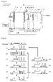
- Fig. 1 illustrates a fundamental constitution of the apparatus for measurement of physical or chemical phenomena according to the present invention
- Fig. 2 is a perspective view thereof (first constitutional example).
- B is for example a semiconductor substrate made of p-type Si (silicon) having a thickness of about 500 mm.
- the semiconductor substrate B has, for example, an insulating film A consisting of a silicon oxide film on which a charge feeding portion 1, a charge feeding regulation portion 2, a sensing portion 3, a barrier portion 4, a sensing charge accumulation portion 5, a threshold portion 6, a floating diffusion 7, reset gates 8a and 9, reset drains 8b and 10, and an output transistor 11 are formed.
- a sensor portion 12 is formed by each member of the charge feeding portion 1, charge feeding regulation portion 2, sensing portion 3, barrier portion 4, reset gate 8a, reset drain 8b, sensing charge accumulation portion 5, and threshold portion 6, and a detection portion is formed by the sensor portion 12, floating diffusion 7, reset gate 9, and reset drain 10.
- the semiconductor substrate B is endowed with resistance to a solution sample etc. by providing it with a resin mold.
- pulse voltage is applied to the charge feeding portion 1, barrier portion 4, threshold portion 6, and reset gates 8a and 9, while direct-current voltage is applied to the other sites, and positive voltage is applied to an MOS structure using a p-type semiconductor, whereby a potential state can be formed in the vicinity of the semiconductor/insulating film interface.
- the sensor portion 12 is formed for example in the following manner.
- the sensing portion 3 is a measurement site having potential changed depending on the magnitude of physical or chemical amount, and in the case of pH measurement, for example, an electrode portion provided with a cell into which an aqueous solution or a measurement object is introduced is formed to generate potential corresponding to the pH of the sample.
- the potential, or a change in the potential is converted into electric charge, and the change in electric charge in the detection portion is outputted and converted by the output transistor 11 of MOS structure.
- the number of the charge feeding portion 1 per one sensing portion 3 is not limited to 1, and a plurality of charge feeding portions 1 may be arranged. As described above, the number, shape or arrangement relationship of sensing portions 3 may be unconditionally determined depending on a measurement object or applications, and when the feed of electric charge to the whole of the sensing portion 3 should be rapidly carried out, loading of electric charge into the sensing portion 3 is preferably dispersed into a plurality of charge feeding portions 1.
- the sensing charge accumulation portion 5 is established depending on the shape of the sensing portion 3 or the charge capacity ratio of the sensing portion 3 to the sensing charge accumulation portion 5, and in Fig. 1, a trapezoid shape is formed so that the contact area with the sensing portion is increased, while the area of the sensing charge accumulation portion 5 is decreased.
- the sensing charge accumulation portion 5 may be formed by n-diffusion layer or p-type substrate as it is.
- the floating diffusion 7 can be made significantly smaller than before because its size is determined on the basis of the portion contacting with the sensing charge accumulation portion 5, and electric charge excluding the electric charge released in the sensing charge accumulation portion 5 is transmitted.
- the floating diffusion 7 is square, but if the shape of the sensing charge accumulation portion 5 is square, the floating diffusion 7 can be formed in a trapezoid shape so that the contacting portion with the sensing charge accumulation portion 5 is increased, while the area of the floating diffusion 7 is decreased.
- the potential of the charge feeding portion 1 is set high (namely, arrow direction is high potential), and no electric charge is fed to the sensing portion 3.
- the amount of electric charge thus accumulated in the sensing portion 3 contains offset charge y and external disturbing component z in addition to the amount x of measurement electric charge, as shown in Fig. 3 (B).
- the electric charge accumulated in the sensing portion 3 is transmitted to the sensing charge accumulation portion 5.
- the amount of electric charge thus transmitted is mainly the amount x of measurement electric charge, but further contains offset charge y or external disturbing component z.
- the above-mentioned (2) to (6) are carried out repeatedly until a predetermined amount of electric charge is accumulated in the floating diffusion 7.
- noises such as external disturbance can be averaged, and the so-called random noise can be substantially reduced.
- the frequency of this repetition is the substantial degree of amplification in this detection system. An accurate description of the degree of amplification will be described later.
- the threshold portion 6 can be in the same state while electric charge is repeatedly accumulated. Given less change in the offset charge, external disturbing noises can be averaged and compensation for offset charge is feasible.
- the potential of the threshold portion 6 is lowered and closed to terminate the inflow of electric charge.
- the potential of the floating diffusion 7 is determined by the amount of electric charge transmitted, so this potential is input into the gate portion in the output transistor 11 of MOS structure, and the drain electric current in this output transistor 11 is measured.
- the reset gate 9 is turned ON, thus supplying electric charge from the reset drain 10 and resetting the potential of the floating diffusion 7 to the potential of the reset drain 10.
- the apparatus is returned to the same state again as in (1). That is, the detection cycle involves repeating the operations in (1) to (9) thereby enabling sequent output of the amount of electric charge corresponding to the state of the potential in the sensing portion 3.
- this measurement apparatus makes use of a charge conversion mechanism in which the sensing portion 3 constituted so as to have charge changed depending on the magnitude of physical or chemical amount is formed on the semiconductor substrate B, and electric charge is fed to the sensing portion 3, and the physical or chemical amount is converted into electric charge corresponding to the size of the sensing portion 3.
- the reset gate 8a arranged on the sensing charge accumulation portion 5 the offset potential or external disturbing component can be released so that the amount of measurement charge can be detected under conditions where factors as noises in detection of the amount of measurement charge are reduced to the lowest degree.
- the electric charge accumulated in the sensing portion 3 is cut by increasing and decreasing the potential of the charge feeding portion 1, but alternatively electric charge may be accumulated in the sensing portion 3 by increasing and decreasing the height of the charge feeding regulation portion 2 while the potential of the charge feeding portion 1 is kept constant, as shown in Fig. 4. That is, the physical or chemical amount can be stably converted into electric charge corresponding to the size of the sensing portion 3 by the following operation.
- the potential of the charge feeding portion 1 is set lower than that of the sensing portion 3, and the potential of the charge feeding regulation portion 2 is set further lower, and the sensing portion 3 is not supplied with electric charge.
- the potential of the charge feeding regulation portion 2 is increased so as to be higher than the potential of the charge feeding portion 1 thereby feeding electric charge to the sensing portion 3.
- the potential of the charge feeding regulation portion 2 is reduced to the state in (1), whereby the fed electric charge is accumulated in the sensing portion 3.
- the electric charge accumulated in the sensing portion 3 is transmitted to the sensing charge accumulation portion 5.
- the amount of electric charge thus transmitted is mainly the amount of measurement electric charge, but further contains some amount of the offset charge or external disturbing component.
- the above-mentioned (2) to (6) are carried out repeatedly until a predetermined amount of electric charge is accumulated in the floating diffusion 7.
- noises such as external disturbance can be averaged, and the so-called random noise can be substantially reduced.
- the frequency of this repetition is the substantial degree of amplification in this detection system.
- the threshold portion 6 can be in the same state while electric charge is repeatedly accumulated. Given less change in the offset charge, external disturbing noises can be averaged and compensation for offset charge is feasible.
- the potential of the threshold portion 6 is lowered and closed to terminate the inflow of electric charge.
- the potential of the floating diffusion 7 is determined by the amount of electric charge transmitted, so this potential is input into the gate portion in the output transistor 11 of MOS structure, and the drain electric current in this output transistor 11 is measured.
- the reset gate 9 is turned ON, thus supplying electric charge from the reset drain 10 and resetting the potential of the floating diffusion 7 to the potential of the reset drain 10.
- the apparatus is returned to the same state again as in (1). That is, the detection cycle involves repeating the operations in (1) to (9) thereby enabling sequent output of the amount of electric charge corresponding to the state of the potential in the sensing portion 3.
- the detection cycle involves repeating the operations in (1) to (9) thereby enabling sequent output of the amount of electric charge corresponding to the state of the potential in the sensing portion 3.
- further improvement in stability can be achieved by retaining a predetermined potential by using the potential of the charge feeding portion 1 as standard.
- electric charge near to the amount of electric charge corresponding substantially to the chemical or physical phenomenon only is transmitted from the electric charge accumulated in the sensing portion 3 to the floating diffusion 7, and can thus processed as an electric charge signal with less noise component.
- the electric charge capacity of the sensing portion 3 preferably has a size exceeding the electric charge capacity of the floating diffusion 7.
- the detection cycle mentioned above is carried out repeatedly until a certain amount of electric charge is accumulated in the floating diffusion 7, and then the electric charge is measured, whereby detection sensitivity can be increased, but the response time is delayed by the accumulation time.
- the rate of change in the potential in the floating diffusion 7 can be increased upon transmission to the floating diffusion 7 with small electric charge capacity, so accurate and highly sensitive measurement is feasible by detecting the rate of change. That is, the apparatus comes to have a function of substantially amplifying a change in the potential in the sensing portion 3 by providing it with a difference in electric charge capacity between the sensing portion 3 and the floating diffusion 7 as charge transmission means.
- sensing portion 3 For increasing the electric charge capacity of the sensing portion 3, there are specific means wherein (1) the area on a plane is increased, (2) a plurality of sensing portions 3 are used, (3) potential is increased, and (4) charge density is increased, from which a suitable means can be selected depending on the state or concentration of a sample as a subject of physical or chemical phenomenon.
- the constitutional example having the semiconductor portion formed the p-type substrate and having an electrode constituted on a sensing charge accumulation portion is illustrated in Fig. 4A.
- the first constitutional example having a sensing charge accumulation portion 5 formed n-type diffusion layer does not need the electrode, on the other side ,the constitution illustrated in Fig. 4A have the same functional ability as above, by having an electrode constituted on the upper site of the p-type substrate to form a sensing charge accumulation portion 53 without forming n-type diffusion layer.
- the metal material constituted on this upper site can be used, for example metal such as Al, W, T or poly-Si. This measurement method is similar to that illustrated in Fig. 3(A), so the description about it is omitted.
- the second constitutional example in the present invention is described.
- the sensing portion 3 is worked as a threshold in place of the charge feeding regulation portion 2 in Fig. 1, thus making the amount of accumulated electric charge changeable so as to correspond to physical or chemical phenomena, in order that the electric charge corresponding to the potential of the sensing portion 3 is accumulated in the sensing charge accumulation portion 5.
- the potential in the sensing portion 3 can be worked as a threshold so that even if the potential of the sensing portion 3 is negatively changed, a change in the amount of electric charge fed from the charge feeding portion 1 to the sensing charge accumulation portion 51 can be taken out according to the chemical or physical phenomenon generated in the sensing portion 3.
- the constitutions and functions of the barrier portion 4, the sensing charge accumulation portion 52 and the portions thereafter are the same as in the first constitutional example.
- electric charge can be accumulated directly in the sensing charge accumulation portion 52 by omitting the sensing charge accumulation portion 51 and the barrier portion 4.
- the potential of the charge feeding portion 1 is set high (namely, arrow direction is high potential), and no electric charge is fed to the sensing charge accumulation portion 51.
- the sensing charge accumulation portion 51 By increasing the potential of the charge feeding portion 1, a part of the fed electric charge overflows so that the amount of electric charge limited by the sensing portion 3 worked as a threshold is accumulated in the sensing charge accumulation portion 51.
- the amount of electric charge thus accumulated in the sensing charge accumulation portion 51 contains an offset charge y and an external disturbing component z in addition to the amount x of measurement electric charge.
- the electric charge accumulated in the sensing charge accumulation portion 51 is transmitted to the sensing charge accumulation portion 52.
- the amount of electric charge thus transmitted is mainly the amount x of measurement electric charge, but further contains the offset charge y or the external disturbing component z.
- the above-mentioned (2) to (6) are carried out repeatedly until a predetermined amount of electric charge is accumulated in the floating diffusion 7. By this repetition, noises such as external disturbance can be averaged, and the so-called random noise can be substantially reduced.
- the frequency of this repetition is the substantial degree of amplification in this detection system.
- the potential of the threshold portion 6 is lowered and closed to terminate the inflow of electric charge.
- the potential of the floating diffusion 7 is determined by the amount of electric charge transmitted, so this potential is input into the gate portion in the output transistor 11 of MOS structure, and the drain electric current in this output transistor 11 is measured.
- the reset gate 9 is turned ON, thus supplying electric charge from the reset drain 10 and resetting the potential of the floating diffusion 7 to the potential of the reset drain 10.
- the apparatus is returned to the same state again as in (1). That is, the detection cycle involves repeating the operations in (1) to (9) thereby enabling sequent output of the amount of electric charge corresponding to the state of the potential in the sensing portion 3.
- this measurement apparatus makes use of a charge conversion mechanism in which the sensing portion 3 constituted so as to have charge changed depending on the magnitude of physical or chemical amount is formed on the semiconductor substrate B, and electric charge is fed via the sensing portion 3 worked as a threshold, and the physical or chemical amount is converted into the amount of electric charge transferred.
- the reset gate 8a arranged on the sensing charge accumulation portion 52 the offset potential or external disturbing component can be released so that the amount of measurement charge can be detected under conditions where factors as noises in detection of the amount of measurement charge are reduced to the lowest degree.
- the electric charge accumulated in the sensing portion 3 is cut by increasing and decreasing the potential of the charge feeding portion 1, but alternatively the potential of the charge feeding portion 1 is kept constant, and electric charge may be accumulated in the sensing charge accumulation portion 51, so as to correspond to the potential of the sensing portion 3 (not shown in the figure).
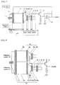
- the third constitutional example in the present invention is illustrated in Fig. 7.
- the output side of the output transistor 11 is provided with a feedback circuit 13 (regulation portion), and the potential of the charge feeding regulation portion 2 is regulated such that the output of the output transistor 11 becomes constant, and the regulation amount is converted into a measurement value.
- the potential of the charge feeding regulation portion 2 is regulated such that the amount of electric charge transferred is made constant by setting the amount of electric charge so as to prevent the electric charge from remaining in the sensing portion 3 or not to influence detection properties even if the electric charge remains.
- the amount of electric charge fed to the sensing portion 3 can be made constant, and the amount of electric charge transferred is made constant.
- the amount of electric charge transferred is made higher than a predetermined value, the influence of the remaining electric charge can be negligible. That is, when the amount of electric charge transferred is higher than a predetermined amount, the transmission power drops with time, and thus the probability of remaining electric charge (the transmission loss) is increased.
- a predetermined amount of transmission loss is generated during actual transmission and the amount of electric charge transferred is lower than a predetermined amount, its influence cannot be negligible.
- the amount of electric charge transferred from the sensing portion 3 to the floating diffusion 7 becomes constant, and as a result, the potential of the floating diffusion 7 becomes constant. That is, when the potential of the charge feeding regulation portion 2 is regulated depending on the change in the potential of the sensing portion 3 accompanying the physical or chemical phenomenon such that the output of the output transistor 11 arranged in the floating diffusion 7 becomes constant, the amount of the regulated potential can become a measurement amount corresponding to the change in the physical or chemical phenomenon, and excellent detection properties having linearity can be obtained.
- the functions of the sensor portion 12 can be stabilized by reducing fluctuation factors. Even if the characteristics of the sensing portion 3 are varied, the above operation can be carried out on the basis of the potential of the charge feeding regulation portion 2 regulated such that the potential difference between the sensing portion 3 and the charge feeding regulation portion 2 is made constant for the same sample. Accordingly, the similar output characteristics can be obtained without strictly regulating the characteristics of the sensing portion 3.
- the apparatus is characterized basically in that two parallel detection systems having the detection portion in the constitutional example described above are constituted, and one threshold portion 6a is connected to the other sensing charge accumulation portion 5b to have the same potential as in.
- the apparatus comprises two detection systems using one charge feeding portion 1 and one charge feeding regulation portion 2 in common, and one detection system A is composed of a sensing portion 3a having potential changed depending on a physical or chemical phenomenon, a barrier portion 4a, a sensing charge accumulation portion 5a, a threshold 6a, a floating diffusion 7, reset gates 8a and 9, reset drains 8b and 10, and an output transistor 11.
- the other detection system B is composed of a sensing portion 3b not responding to a physical or chemical phenomenon, a barrier portion 4b, a sensing charge accumulation portion 5b, and a threshold portion 6b.
- the sensing portions 3a and 3b form basically the same structure, and are provided preferably with a film or site having a different responding property to a physical or chemical phenomenon. This is because the compensation function of the detection system B can be improved by generating the same change in offset charge and external disturbing component.
- the electric charge signal in the detection system A corresponds to “detection signal + offset signal + external disturbing signal”
- the electric charge signal in the detection system B corresponds to “offset signal + external disturbing signal”. Accordingly, the true “detection signal” can be obtained by determining the difference between the two. That is, in the present invention, the amount of electric charge to be accumulated in the sensing charge accumulation portion 5a in the detection system A corresponds to the electric charge signal in the detection system A described above, and the amount of electric charge accumulated in the sensing charge accumulation portion 5b in the detection system B corresponds to the electric charge signal in the detection system B described above.
- the threshold portion 6a in the detection system A and the sensing charge accumulation portion 5b in the detection system B are connected at the same potential, and thus the amount of electric charge to be accumulated in the sensing charge accumulation portion 5a in the detection system A minus the amount of electric charge accumulated in the sensing charge accumulation portion 5b in the detection system B, that is, the amount of electric charge corresponding to the detection signal only is transmitted via the threshold 6a in the detection system A to the floating diffusion 7. Accordingly, the truly required detection signal only can be taken out with high accuracy by effectively using the compensation function of the detection system B.
- the potential of the charge feeding portion 1 is set high (namely, arrow direction is high potential), and no electric charge is fed to the sensing portions 3a and 3b.
- the amount of electric charge thus accumulated in the sensing portion 3a in the detection system A contains an offset charge y and an external disturbing component z in addition to the amount x of measurement electric charge as shown in Fig. 3 (B), and the amount of electric charge corresponding to the offset charge y and the external disturbing component z is accumulated in the sensing portion 3b in the detection system.
- the electric charge accumulated in the sensing portions 3a and 3b is transmitted to the sensing charge accumulation portions 5a and 5b.
- the potential of the barrier 4a in the detection system A is increased with slight delay after the potential of the barrier portion 4b in the detection system B is increased.
- the potential of the threshold portion 6a becomes the same level as the potential of the sensing charge accumulation portion 5b, so the potential of the threshold portion 6a is gradually decreased in accordance with the increase in the amount of electric charge accumulated in the sensing charge accumulation portion 5b.
- the potential of the threshold portion 6b in the detection system A is increased thereby forming a space for accumulating the electric charge from the sensing portion 3a, thus preventing the electric charge from being transmitted by leakage into the floating diffusion 7.
- the delay time can be previously established by measuring or estimating the amount x of the measurement electric charge, the offset charge y and the external disturbing component z.
- the sensing charge accumulation portions 5a and 5b By decreasing the potential of the barrier portions 4a and 4b, a part of the electric charge accumulated is accumulated in the sensing charge accumulation portions 5a and 5b.
- the amount of electric charge in the sensing charge accumulation portion 5b in the detection system B contains the offset charge y or the external disturbing component z.
- the amount of electric charge accumulated in the sensing charge accumulation portion 5a in the detection system A contains the offset charge y or the external disturbing component y originally in addition to the amount x of the measurement electric charge.
- the amount x of the measurement electric charge overflows from the threshold portion 6a and is transmitted to the floating diffusion 7.
- the reset gate 8a By increasing the potential of the reset gate 8a, the electric charge accumulated in the sensing charge accumulation portion 5a in the detection system A is released to the outside.
- the threshold portion 6b By increasing the potential of the threshold portion 6b, the electric charge accumulated in the sensing charge accumulation portion 5b in the detection system B is released to the outside.
- the above-mentioned (2) to (7) are carried out repeatedly until a predetermined amount of electric charge is accumulated in the floating diffusion 7.
- noises such as external disturbance can be averaged, and the so-called random noise can be substantially reduced.
- the frequency of this repetition is the substantially degree of amplification in this detection system.
- the amount of detected electric charge only can be extracted and accumulated, and thus the S/N ratio is significantly improved.
- the potential of the threshold portion 6a is lowered and closed to terminate the inflow of electric charge.
- the potential of the floating diffusion 7 is determined by the amount of electric charge transmitted, so this potential is input into the gate portion in the output transistor 11 of MOS structure, and the drain electric current in this output transistor 11 is measured.
- the reset gate 9 is turned ON, thus supplying electric charge from the reset drain 10 and resetting the potential of the floating diffusion 7 to the potential of the reset drain 10.
- the apparatus is returned to the same state again as in (1). That is, the detection cycle involves repeating the operations in (1) to (10) thereby enabling sequent output of the amount of electric charge corresponding to the state of the potential in the sensing portion 3a.
- the amount of electric charge free from noise components is taken out from the electric charge from the sensing portion 3a constituted to have potential changed depending on the magnitude of physical or chemical amount, whereby the amount of measurement charge can be detected under conditions where factors as noises in detection of the amount of the measurement charge are reduced to the lowest degree.
- the electric charge accumulated in the sensing portion 3 is cut by increasing and decreasing the potential of the charge feeding portion 1, but alternatively the potential of the charge feeding portion 1 is kept constant, and electric charge may be accumulated in the sensing portions 3a and 3b by increasing and decreasing the height of the charge feeding regulation portion 2 (not shown in the figure).
- each detection system is based on the second constitutional example, is now described, while in the fourth constitutional example, each detection system is based on the constitution of the first constitutional example.
- the fifth constitutional example is the same as in the fourth constitutional example in respect of the fundamental constitution, but is different in that the amount of electric charge fed to the sensing charge accumulation portions 51a and 51b is determined with a pair of sensing portions 3a and 3b worked as thresholds in two detection systems A and B in place of the charge feeding regulation portion.
- the change, corresponding to the chemical or physical phenomenon, of the amount of electric charge fed from the charge feeding portion 1 to the sensing charge accumulation portions 51a and 51b can be taken out in the detection system A with the sensing portion 3a worked as a threshold, while the change not corresponding to the chemical or physical phenomenon can be taken out in the detection system B with the sensing portion 3b worked as a threshold.
- the sensing charge accumulation portions 51a and 51b preferably have the same potential. This is because the offset charges y in the respective detection systems can be made equal such that the compensation function can be improved.
- the amount of electric charge fed to the sensing charge accumulation portion 51a in the detection system A is mainly the amount x of the measurement electric charge, but further contains the offset charge y or the external disturbing component z.
- the amount of electric charge fed to the sensing charge accumulation portion 51b in the detection system B contains the offset charge y or the external disturbing component z.
- the threshold portion 6a in the detection system A and the sensing charge accumulation portion 52b in the detection system B are connected at the same potential, and thus the amount of electric charge to be accumulated in the sensing charge accumulation portion 52a in the detection system A minus the amount of electric charge accumulated in the sensing charge accumulation portion 52b in the detection system B, that is, the amount x of the measurement electric charge only is transmitted via the threshold portion 6a in the detection system A to the floating diffusion 7. Accordingly, only the truly required amount x of the measurement electric value, that is, the detection signal only can be taken out with high accuracy by effectively using the compensation function of the detection system B.
- the apparatus may have a CCD function of transferring electric charges one after another from a plurality of sensors via the charge transmission portion to one floating diffusion, whereby one- or two-dimensional distribution of physical or chemical phenomena can be converted easily into an image.
- a CCD function of transferring electric charges one after another from a plurality of sensors via the charge transmission portion to one floating diffusion, whereby one- or two-dimensional distribution of physical or chemical phenomena can be converted easily into an image.
- the sixth constitutional example as shown in Fig. 11 is feasible.
- the apparatus comprises a plurality of sensor portions 12 (a, a), 12 (a, b), ..., a charge transmission portion 16 for transmitting, in the array direction, the electric charge converted in each sensor portion, one floating diffusion 7 for further transmitting the transmitted electric charge, and an output transistor 11 for converting the transmitted electric charge into an output signal.
- gates in connection portions between the sensor portions 12 (a, a), 12 (a, b), ... and the charge transmission portion 16 are opened one after another to supply the accumulated electric charge which is then transmitted via the transmission path of the charge transmission portion 16 by turning the CCD driving potential ON-OFF in order.
- CCD in the transmission portion 16 one-phase driving, two-phase driving or four-phase driving can be suitably selected depending on the amount of electric charge transmitted.
- the efficiency of transmission becomes problematic as the number of sensor portions 12 is increased, and in this case, a bulk channel having high efficiency of transmission is preferably used as the transmission path.
- the charge transmitted is transmitted to the floating diffusion 7, to change the potential of the floating diffusion 7. This change in the potential is inputted as detection output into the gate of the output transistor 11.
- the CCD has excellent properties in respect of high S/N ratio, rate of transfer, efficiency of transmission, and operativeness, and is very useful in actuating a plurality of electrodes. That is, the CCD is also superior in that a plurality of electrodes constituting the CCD can perform the functions of the sensing charge accumulation portion 5, the barrier portion 4 or the threshold portion 6, to achieve higher transmission.
- the CCD is also useful in that since there is no necessity for providing a difference among voltages applied to the respective electrodes, there is no necessity for limitation of the potential difference between the sensing portion 3 and the floating diffusion 7 or for limitation of the number of electrodes.
- the number of electrodes driven during transmission of electric charge can be changed depending on the amount of electric charge accumulated in the sensing portion 3 thereby transmitting electric charge under the optimum conditions. That is, when the amount of electric charge transmitted is too high, a plurality of electrodes are driven whereby electric charge not transmitted can be eliminated. When the amount of electric charge transmitted is low, one electrode can be driven whereby the remaining electric charge in the electrode portion can be eliminated, thus eliminating a cause for measurement errors.
- the present invention can be applied preferably not only in two-dimensional distribution measurement of ion concentration in various samples such as solution, but also to the following fields:
- the measurement object may be a gas, liquid, solid and powder
- the present invention can be applied to chemical sensing reacting selectively by a specific responsive layer of the sensor portion, and any phenomena showing charge fluctuation in interfacial phenomena by physical contact, and for example, distribution of a transient phenomenon in liquid stream or in an instant chemical reaction can be obtained as a chemical image of high density and high qualities.
- the present invention is useful not only in real-time imaging of titration phenomenon but also in another kind of analysis and display by imaging software, and also useful in pocket cameras.
- a method of or for measuring a physical or chemical phenomenon ist provided.
- the inventive method comprises steps of feeding electric charge from a charge feeding portion 1 to a sensing portion 3 that is having potential changed depending on the magnitude of physical or chemical property/quantity, removing the fed electric charge via a floating diffusion 7 from the sensing portion 3, and detecting the amount of the fed electric charge thereby measuring the physical or chemical phenomenon, or wherein the sensing portion 3 has the function working as a barrier changing the electric charge fed from the charge feeding portion 1.
- Said method has and/or realizes a function which is also called a charge transfer function of allowing the electric charge from the sensing portion 3 to be accumulated in a stage before the floating diffusion 7, to release a part thereof, and simultaneously transmitting, to the floating diffusion 7, the amount of electric charge containing the electric charge corresponding to the potential corresponding to the magnitude of physical or chemical property/quantity, wherein the release amount of electric charge is changeable.
- the inventive method may further comprise a step of measuring a physical or chemical phenomenon by using a pair of detection systems consisting of a detection system A and a detection system B, said detection system A having a sensing portion 3, having potential changed depending on the magnitude of physical or chemical property/quantity, and having or realizing said charge transfer function, and said detection system B having a sensing portion 3 not responding to a change in physical or chemical property/ quantity and having or realizing said said charge transfer function as that of the detection system A except for the sensing portion 3, wherein the amount of electric charge released in the detection system A is changed by synchronizing with the amount of the electric charge accumulated in the stage before the floating diffusion 7 in the detection system B.
- an apparatus for measuring a physical or chemical phenomenon is provided.
- the inventive apparatus comprises a charge feeding portion 1 for feeding electric charge to a sensing portion 3, a sensing portion 3 that is having voltage changed depending on the magnitude of physical or chemical property/quantity, and a detection portion consisting of a floating diffusion 7 for removing electric charge fed to the sensing portion 3, or wherein the sensing portion 3 has the function of working as a barrier changing the electric charge fed from the charge feeding portion 1.
- the apparatus may further comprise between the sensing portion 3 and the floating diffusion 7 a sensing charge accumulation portion 5 for accumulating electric charge transmitted from the sensing portion 3 and having a reset gate 8a for releasing a part of the electric charge accumulated, and a barrier portion 6 for transmitting the remaining electric charge to the floating diffusion 7.
- the inventive apparatus may further comprise at least a pair of detection systems having a charge feeding portion 1, a sensing charge accumulation portion 5, and a reset gate 8a of the same structure as above.
- the inventive apparatus may further comprise a detection system A having a sensing portion 3a having potential changed depending on the magnitude of physical or chemical property/quantity, wherein a part of the electric charge fed to the sensing portion 3a is transmitted via the sensing charge accumulation portion 5a and a barrier portion 6a to the floating diffusion 7, and a detection system B having a sensing portion 3b not responding to a change in physical or chemical property / quantity and having the same function as in the detection system A except for the sensing portion3a, wherein the amount of electric charge transmitted from the barrier portion 6a in the detection system A is changed by synchronizing with the amount of electric charge accumulated in the sensing charge accumulation portion 5b in the detection system B.
- the inventive apparatus may further be provided with a charge transmission means 16 between the sensing charge accumulation portion and the floating diffusion 7, wherein the charge transmission means 16 is a charge coupled device, and wherein the electric charge in a plurality of sensing charge accumulation portions 5a is transmitted to one floating diffusion 7.
- the inventive apparatus may further comprise the detection portion having n-diffusion layer formed, or, when the semiconductor portion is p-type substrate, having an electrode constituted on the upper site of the p-type substrate to form a sensing charge accumulation portion 53.
Applications Claiming Priority (2)
| Application Number | Priority Date | Filing Date | Title |
|---|---|---|---|
| JP2004358803 | 2004-12-10 | ||
| JP2005225505A JP4678676B2 (ja) | 2004-12-10 | 2005-08-03 | 物理現象または化学現象の測定方法または測定装置 |
Publications (1)
| Publication Number | Publication Date |
|---|---|
| EP1669749A1 true EP1669749A1 (de) | 2006-06-14 |
Family
ID=35985424
Family Applications (1)
| Application Number | Title | Priority Date | Filing Date |
|---|---|---|---|
| EP05027011A Withdrawn EP1669749A1 (de) | 2004-12-10 | 2005-12-09 | FET basiertes Verfahren und Vorrichtung zur Messung physischer oder chemischer Phänomene |
Country Status (3)
| Country | Link |
|---|---|
| US (1) | US7424372B2 (de) |
| EP (1) | EP1669749A1 (de) |
| JP (1) | JP4678676B2 (de) |
Cited By (22)
| Publication number | Priority date | Publication date | Assignee | Title |
|---|---|---|---|---|
| JP2016188867A (ja) * | 2010-06-30 | 2016-11-04 | ライフ テクノロジーズ コーポレーション | Isfetアレイをテストする方法及び装置 |
| US9823217B2 (en) | 2013-03-15 | 2017-11-21 | Life Technologies Corporation | Chemical device with thin conductive element |
| US9835585B2 (en) | 2013-03-15 | 2017-12-05 | Life Technologies Corporation | Chemical sensor with protruded sensor surface |
| US9841398B2 (en) | 2013-01-08 | 2017-12-12 | Life Technologies Corporation | Methods for manufacturing well structures for low-noise chemical sensors |
| US9852919B2 (en) | 2013-01-04 | 2017-12-26 | Life Technologies Corporation | Methods and systems for point of use removal of sacrificial material |
| US9927393B2 (en) | 2009-05-29 | 2018-03-27 | Life Technologies Corporation | Methods and apparatus for measuring analytes |
| US9951382B2 (en) | 2006-12-14 | 2018-04-24 | Life Technologies Corporation | Methods and apparatus for measuring analytes using large scale FET arrays |
| US9958415B2 (en) | 2010-09-15 | 2018-05-01 | Life Technologies Corporation | ChemFET sensor including floating gate |
| US9960253B2 (en) | 2010-07-03 | 2018-05-01 | Life Technologies Corporation | Chemically sensitive sensor with lightly doped drains |
| US9964515B2 (en) | 2008-10-22 | 2018-05-08 | Life Technologies Corporation | Integrated sensor arrays for biological and chemical analysis |
| US9970984B2 (en) | 2011-12-01 | 2018-05-15 | Life Technologies Corporation | Method and apparatus for identifying defects in a chemical sensor array |
| US9989489B2 (en) | 2006-12-14 | 2018-06-05 | Life Technnologies Corporation | Methods for calibrating an array of chemically-sensitive sensors |
| US9995708B2 (en) | 2013-03-13 | 2018-06-12 | Life Technologies Corporation | Chemical sensor with sidewall spacer sensor surface |
| US10077472B2 (en) | 2014-12-18 | 2018-09-18 | Life Technologies Corporation | High data rate integrated circuit with power management |
| US10422767B2 (en) | 2013-03-15 | 2019-09-24 | Life Technologies Corporation | Chemical sensor with consistent sensor surface areas |
| US10458942B2 (en) | 2013-06-10 | 2019-10-29 | Life Technologies Corporation | Chemical sensor array having multiple sensors per well |
| US10481123B2 (en) | 2010-06-30 | 2019-11-19 | Life Technologies Corporation | Ion-sensing charge-accumulation circuits and methods |
| US10605767B2 (en) | 2014-12-18 | 2020-03-31 | Life Technologies Corporation | High data rate integrated circuit with transmitter configuration |
| US10641729B2 (en) | 2010-06-30 | 2020-05-05 | Life Technologies Corporation | Column ADC |
| US10718733B2 (en) | 2009-05-29 | 2020-07-21 | Life Technologies Corporation | Methods and apparatus for measuring analytes |
| US11307166B2 (en) | 2010-07-01 | 2022-04-19 | Life Technologies Corporation | Column ADC |
| US11339430B2 (en) | 2007-07-10 | 2022-05-24 | Life Technologies Corporation | Methods and apparatus for measuring analytes using large scale FET arrays |
Families Citing this family (8)
| Publication number | Priority date | Publication date | Assignee | Title |
|---|---|---|---|---|
| KR101269508B1 (ko) * | 2005-03-11 | 2013-05-30 | 고꾸리쯔 다이가꾸 호우징 도요하시 기쥬쯔 가가꾸 다이가꾸 | 누적형 화학·물리현상 검출장치 |
| JP5077799B2 (ja) * | 2008-03-25 | 2012-11-21 | 国立大学法人豊橋技術科学大学 | 化学・物理現象検出装置及びその制御方法 |
| EP2733483B1 (de) * | 2011-07-14 | 2020-04-29 | National University Corporation Toyohashi University of Technology | Verfahren zum nachweis chemischer oder physikalischer phänomene und vorrichtung dafür |
| JP6228098B2 (ja) * | 2014-10-20 | 2017-11-08 | シャープ株式会社 | 化学・物理現象検出装置及びその製造方法 |
| US10309922B2 (en) * | 2015-03-19 | 2019-06-04 | National University Corporation Toyohashi University Of Technology | Device for detecting chemical/physical phenomenon |
| US11846603B2 (en) | 2018-05-25 | 2023-12-19 | University Public Corporation Osaka | Chemical sensor |
| JP2020094913A (ja) * | 2018-12-13 | 2020-06-18 | 国立大学法人豊橋技術科学大学 | pH検出装置 |
| US11913971B2 (en) * | 2021-02-24 | 2024-02-27 | Globalfoundries U.S. Inc. | Motion-sensitive field effect transistor, motion detection system, and method |
Citations (5)
| Publication number | Priority date | Publication date | Assignee | Title |
|---|---|---|---|---|
| EP0881486A2 (de) * | 1997-05-29 | 1998-12-02 | Horiba, Ltd. | Verfahren zur Messung von physikalischen Phänomenen oder chemischen Phänomenen und Vorrichtung dafür |
| DE19857851A1 (de) * | 1998-01-14 | 1999-07-22 | Horiba Ltd | Detektionsgerät für physikalische und/oder chemische Größen |
| EP1130389A1 (de) * | 2000-02-29 | 2001-09-05 | Horiba, Ltd. | Chemischer CCD Sensor zur molekularen Erkennung |
| EP1278060A1 (de) * | 2001-06-29 | 2003-01-22 | Horiba, Ltd. | CCD Sensor |
| WO2003043683A1 (en) * | 2001-11-13 | 2003-05-30 | Applied Medical Resources Corporation | Multi-seal trocar system |
Family Cites Families (11)
| Publication number | Priority date | Publication date | Assignee | Title |
|---|---|---|---|---|
| JP2571016B2 (ja) | 1994-04-27 | 1997-01-16 | 日本電気株式会社 | ガス放電表示パネルの製造方法 |
| JP3559640B2 (ja) * | 1996-02-27 | 2004-09-02 | キヤノン株式会社 | 光電変換装置 |
| JP3440722B2 (ja) * | 1996-09-20 | 2003-08-25 | ソニー株式会社 | 固体撮像装置およびその駆動方法並びにカメラ |
| JP3608903B2 (ja) * | 1997-04-02 | 2005-01-12 | パイオニア株式会社 | 面放電型プラズマディスプレイパネルの駆動方法 |
| US5998935A (en) * | 1997-09-29 | 1999-12-07 | Matsushita Electric Industrial Co., Ltd. | AC plasma display with dual discharge sites and contrast enhancement bars |
| US5852347A (en) * | 1997-09-29 | 1998-12-22 | Matsushita Electric Industries | Large-area color AC plasma display employing dual discharge sites at each pixel site |
| JP2000065786A (ja) * | 1998-08-20 | 2000-03-03 | Horiba Ltd | 電解液のpH分布測定装置 |
| JP2001050897A (ja) * | 1999-08-10 | 2001-02-23 | Horiba Ltd | 化学二次元分布測定装置 |
| JP3623728B2 (ja) * | 2000-09-27 | 2005-02-23 | 独立行政法人科学技術振興機構 | 累積型化学・物理現象検出装置 |
| WO2003042683A1 (en) * | 2001-11-16 | 2003-05-22 | Bio-X Inc. | Fet type sensor, ion density detecting method comprising this sensor, and base sequence detecting method |
| JP3832441B2 (ja) * | 2002-04-08 | 2006-10-11 | 松下電工株式会社 | 強度変調光を用いた空間情報の検出装置 |
-
2005
- 2005-08-03 JP JP2005225505A patent/JP4678676B2/ja not_active Expired - Fee Related
- 2005-11-29 US US11/289,819 patent/US7424372B2/en not_active Expired - Fee Related
- 2005-12-09 EP EP05027011A patent/EP1669749A1/de not_active Withdrawn
Patent Citations (5)
| Publication number | Priority date | Publication date | Assignee | Title |
|---|---|---|---|---|
| EP0881486A2 (de) * | 1997-05-29 | 1998-12-02 | Horiba, Ltd. | Verfahren zur Messung von physikalischen Phänomenen oder chemischen Phänomenen und Vorrichtung dafür |
| DE19857851A1 (de) * | 1998-01-14 | 1999-07-22 | Horiba Ltd | Detektionsgerät für physikalische und/oder chemische Größen |
| EP1130389A1 (de) * | 2000-02-29 | 2001-09-05 | Horiba, Ltd. | Chemischer CCD Sensor zur molekularen Erkennung |
| EP1278060A1 (de) * | 2001-06-29 | 2003-01-22 | Horiba, Ltd. | CCD Sensor |
| WO2003043683A1 (en) * | 2001-11-13 | 2003-05-30 | Applied Medical Resources Corporation | Multi-seal trocar system |
Non-Patent Citations (1)
| Title |
|---|
| SAWADA K ET AL: "Highly sensitive ion sensors using charge transfer technique", SENSORS AND ACTUATORS B, ELSEVIER SEQUOIA S.A., LAUSANNE, CH, vol. 98, no. 1, 1 March 2004 (2004-03-01), pages 69 - 72, XP004493656, ISSN: 0925-4005 * |
Cited By (43)
| Publication number | Priority date | Publication date | Assignee | Title |
|---|---|---|---|---|
| US9989489B2 (en) | 2006-12-14 | 2018-06-05 | Life Technnologies Corporation | Methods for calibrating an array of chemically-sensitive sensors |
| US10502708B2 (en) | 2006-12-14 | 2019-12-10 | Life Technologies Corporation | Chemically-sensitive sensor array calibration circuitry |
| US10633699B2 (en) | 2006-12-14 | 2020-04-28 | Life Technologies Corporation | Methods and apparatus for measuring analytes using large scale FET arrays |
| US10203300B2 (en) | 2006-12-14 | 2019-02-12 | Life Technologies Corporation | Methods and apparatus for measuring analytes using large scale FET arrays |
| US9951382B2 (en) | 2006-12-14 | 2018-04-24 | Life Technologies Corporation | Methods and apparatus for measuring analytes using large scale FET arrays |
| US11732297B2 (en) * | 2006-12-14 | 2023-08-22 | Life Technologies Corporation | Methods and apparatus for measuring analytes using large scale FET arrays |
| US20220340965A1 (en) * | 2006-12-14 | 2022-10-27 | Life Technologies Corporation | Methods and Apparatus for Measuring Analytes Using Large Scale FET Arrays |
| US11435314B2 (en) | 2006-12-14 | 2022-09-06 | Life Technologies Corporation | Chemically-sensitive sensor array device |
| US10816506B2 (en) | 2006-12-14 | 2020-10-27 | Life Technologies Corporation | Method for measuring analytes using large scale chemfet arrays |
| US11339430B2 (en) | 2007-07-10 | 2022-05-24 | Life Technologies Corporation | Methods and apparatus for measuring analytes using large scale FET arrays |
| US11137369B2 (en) | 2008-10-22 | 2021-10-05 | Life Technologies Corporation | Integrated sensor arrays for biological and chemical analysis |
| US9964515B2 (en) | 2008-10-22 | 2018-05-08 | Life Technologies Corporation | Integrated sensor arrays for biological and chemical analysis |
| US9927393B2 (en) | 2009-05-29 | 2018-03-27 | Life Technologies Corporation | Methods and apparatus for measuring analytes |
| US10809226B2 (en) | 2009-05-29 | 2020-10-20 | Life Technologies Corporation | Methods and apparatus for measuring analytes |
| US10718733B2 (en) | 2009-05-29 | 2020-07-21 | Life Technologies Corporation | Methods and apparatus for measuring analytes |
| US11768171B2 (en) | 2009-05-29 | 2023-09-26 | Life Technologies Corporation | Methods and apparatus for measuring analytes |
| US11692964B2 (en) | 2009-05-29 | 2023-07-04 | Life Technologies Corporation | Methods and apparatus for measuring analytes |
| US10481123B2 (en) | 2010-06-30 | 2019-11-19 | Life Technologies Corporation | Ion-sensing charge-accumulation circuits and methods |
| JP2016188867A (ja) * | 2010-06-30 | 2016-11-04 | ライフ テクノロジーズ コーポレーション | Isfetアレイをテストする方法及び装置 |
| US10641729B2 (en) | 2010-06-30 | 2020-05-05 | Life Technologies Corporation | Column ADC |
| US11231451B2 (en) | 2010-06-30 | 2022-01-25 | Life Technologies Corporation | Methods and apparatus for testing ISFET arrays |
| US11307166B2 (en) | 2010-07-01 | 2022-04-19 | Life Technologies Corporation | Column ADC |
| US9960253B2 (en) | 2010-07-03 | 2018-05-01 | Life Technologies Corporation | Chemically sensitive sensor with lightly doped drains |
| US9958415B2 (en) | 2010-09-15 | 2018-05-01 | Life Technologies Corporation | ChemFET sensor including floating gate |
| US9958414B2 (en) | 2010-09-15 | 2018-05-01 | Life Technologies Corporation | Apparatus for measuring analytes including chemical sensor array |
| US9970984B2 (en) | 2011-12-01 | 2018-05-15 | Life Technologies Corporation | Method and apparatus for identifying defects in a chemical sensor array |
| US10598723B2 (en) | 2011-12-01 | 2020-03-24 | Life Technologies Corporation | Method and apparatus for identifying defects in a chemical sensor array |
| US10365321B2 (en) | 2011-12-01 | 2019-07-30 | Life Technologies Corporation | Method and apparatus for identifying defects in a chemical sensor array |
| US9852919B2 (en) | 2013-01-04 | 2017-12-26 | Life Technologies Corporation | Methods and systems for point of use removal of sacrificial material |
| US9841398B2 (en) | 2013-01-08 | 2017-12-12 | Life Technologies Corporation | Methods for manufacturing well structures for low-noise chemical sensors |
| US10436742B2 (en) | 2013-01-08 | 2019-10-08 | Life Technologies Corporation | Methods for manufacturing well structures for low-noise chemical sensors |
| US9995708B2 (en) | 2013-03-13 | 2018-06-12 | Life Technologies Corporation | Chemical sensor with sidewall spacer sensor surface |
| US9823217B2 (en) | 2013-03-15 | 2017-11-21 | Life Technologies Corporation | Chemical device with thin conductive element |
| US10422767B2 (en) | 2013-03-15 | 2019-09-24 | Life Technologies Corporation | Chemical sensor with consistent sensor surface areas |
| US9835585B2 (en) | 2013-03-15 | 2017-12-05 | Life Technologies Corporation | Chemical sensor with protruded sensor surface |
| US10816504B2 (en) | 2013-06-10 | 2020-10-27 | Life Technologies Corporation | Chemical sensor array having multiple sensors per well |
| US11774401B2 (en) | 2013-06-10 | 2023-10-03 | Life Technologies Corporation | Chemical sensor array having multiple sensors per well |
| US10458942B2 (en) | 2013-06-10 | 2019-10-29 | Life Technologies Corporation | Chemical sensor array having multiple sensors per well |
| US11499938B2 (en) | 2013-06-10 | 2022-11-15 | Life Technologies Corporation | Chemical sensor array having multiple sensors per well |
| US10077472B2 (en) | 2014-12-18 | 2018-09-18 | Life Technologies Corporation | High data rate integrated circuit with power management |
| US11536688B2 (en) | 2014-12-18 | 2022-12-27 | Life Technologies Corporation | High data rate integrated circuit with transmitter configuration |
| US10605767B2 (en) | 2014-12-18 | 2020-03-31 | Life Technologies Corporation | High data rate integrated circuit with transmitter configuration |
| US10767224B2 (en) | 2014-12-18 | 2020-09-08 | Life Technologies Corporation | High data rate integrated circuit with power management |
Also Published As
| Publication number | Publication date |
|---|---|
| JP2006189416A (ja) | 2006-07-20 |
| US7424372B2 (en) | 2008-09-09 |
| JP4678676B2 (ja) | 2011-04-27 |
| US20060129332A1 (en) | 2006-06-15 |
Similar Documents
| Publication | Publication Date | Title |
|---|---|---|
| EP1669749A1 (de) | FET basiertes Verfahren und Vorrichtung zur Messung physischer oder chemischer Phänomene | |
| EP2625514B1 (de) | Isfet-gerät | |
| JP2006284225A (ja) | ポテンシャルの測定方法および測定装置 | |
| US6255678B1 (en) | Apparatus for measuring physical and chemical phenomena | |
| Hizawa et al. | Fabrication of a two-dimensional pH image sensor using a charge transfer technique | |
| Matsuo et al. | Charge Transfer Type pH Sensor with Super High Sensitivity | |
| Schienle et al. | A fully electronic DNA sensor with 128 positions and in-pixel A/D conversion | |
| JP4195859B2 (ja) | Fet型センサと、そのセンサを用いたイオン濃度検出方法及び塩基配列検出方法 | |
| US20140234981A1 (en) | Double gate ion sensitive field effect transistor | |
| EP1843152B1 (de) | Verfahren zur Erkennung von Biomolekülen mit dem gleichen Feldeffekttransistor auf dessen Gate-Messoberfläche. | |
| JP2014520568A (ja) | ナノ細孔ポリヌクレオチド配列決定、その他の用途のための補償型パッチクランプ増幅器 | |
| TW201508271A (zh) | 具有背景電流操縱之背側受激感測器 | |
| Li et al. | Direct measurement of K+ ion efflux from neuronal cells using a graphene-based ion sensitive field effect transistor | |
| JP4641444B2 (ja) | 物理現象または化学現象に係るポテンシャル測定装置 | |
| JP2007255906A (ja) | 電極式溶液測定方法および電極式溶液測定装置 | |
| Teng et al. | Sensing characteristic enhancement of CMOS-based ISFETs with three-dimensional extended-gate architecture | |
| Sawada et al. | Smart microfluidic electrochemical DNA sensors with signal processing circuits | |
| JP2005337806A (ja) | 物理現象または化学現象の測定方法または測定装置 | |
| JP4700335B2 (ja) | 物理現象または化学現象の測定方法および測定装置 | |
| Okumura et al. | Development of H 2 O 2 image sensor for GABA and glutamate imaging | |
| Hizawa et al. | Fabrication of 2D pH CMOS image sensors and real time imaging of chemical reaction | |
| Lee et al. | High Performance Blood Glucose Sensor using Charge Transfer Technique | |
| Yamazaki et al. | Design and Fabrication of Complementary Metal–Oxide–Semiconductor Sensor Chip for Electrochemical Measurement | |
| Takahashi et al. | Proposition and fabrication of Amplified Redox Sensor (ARS) for high sensitive chemical analysis | |
| Cho et al. | High-Resolution DNA Binding Kinetics Measurements with Double Gate FD-SOI Transistors |
Legal Events
| Date | Code | Title | Description |
|---|---|---|---|
| PUAI | Public reference made under article 153(3) epc to a published international application that has entered the european phase |
Free format text: ORIGINAL CODE: 0009012 |
|
| AK | Designated contracting states |
Kind code of ref document: A1 Designated state(s): AT BE BG CH CY CZ DE DK EE ES FI FR GB GR HU IE IS IT LI LT LU LV MC NL PL PT RO SE SI SK TR |
|
| AX | Request for extension of the european patent |
Extension state: AL BA HR MK YU |
|
| 17P | Request for examination filed |
Effective date: 20061120 |
|
| 17Q | First examination report despatched |
Effective date: 20061222 |
|
| AKX | Designation fees paid |
Designated state(s): DE FR GB |
|
| STAA | Information on the status of an ep patent application or granted ep patent |
Free format text: STATUS: THE APPLICATION IS DEEMED TO BE WITHDRAWN |
|
| 18D | Application deemed to be withdrawn |
Effective date: 20100701 |