EP1668706B1 - Method for metal replacement gate of high performance device - Google Patents
Method for metal replacement gate of high performance device Download PDFInfo
- Publication number
- EP1668706B1 EP1668706B1 EP04786558A EP04786558A EP1668706B1 EP 1668706 B1 EP1668706 B1 EP 1668706B1 EP 04786558 A EP04786558 A EP 04786558A EP 04786558 A EP04786558 A EP 04786558A EP 1668706 B1 EP1668706 B1 EP 1668706B1
- Authority
- EP
- European Patent Office
- Prior art keywords
- layer
- metal
- gate
- tungsten
- substrate
- Prior art date
- Legal status (The legal status is an assumption and is not a legal conclusion. Google has not performed a legal analysis and makes no representation as to the accuracy of the status listed.)
- Not-in-force
Links
- 229910052751 metal Inorganic materials 0.000 title claims abstract description 89
- 239000002184 metal Substances 0.000 title claims abstract description 89
- 238000000034 method Methods 0.000 title claims abstract description 82
- WFKWXMTUELFFGS-UHFFFAOYSA-N tungsten Chemical compound [W] WFKWXMTUELFFGS-UHFFFAOYSA-N 0.000 claims abstract description 55
- 229910052721 tungsten Inorganic materials 0.000 claims abstract description 55
- 239000010937 tungsten Substances 0.000 claims abstract description 55
- 239000000758 substrate Substances 0.000 claims abstract description 43
- 230000004888 barrier function Effects 0.000 claims abstract description 27
- 125000006850 spacer group Chemical group 0.000 claims abstract description 27
- 238000009792 diffusion process Methods 0.000 claims abstract description 26
- 239000004065 semiconductor Substances 0.000 claims abstract description 20
- 239000000463 material Substances 0.000 claims description 35
- 229910021420 polycrystalline silicon Inorganic materials 0.000 claims description 35
- 229920005591 polysilicon Polymers 0.000 claims description 34
- 238000000151 deposition Methods 0.000 claims description 27
- 239000002243 precursor Substances 0.000 claims description 12
- 150000004767 nitrides Chemical class 0.000 claims description 11
- VYPSYNLAJGMNEJ-UHFFFAOYSA-N Silicium dioxide Chemical compound O=[Si]=O VYPSYNLAJGMNEJ-UHFFFAOYSA-N 0.000 claims description 9
- 229910008940 W(CO)6 Inorganic materials 0.000 claims description 9
- 150000002736 metal compounds Chemical class 0.000 claims description 9
- BASFCYQUMIYNBI-UHFFFAOYSA-N platinum Chemical compound [Pt] BASFCYQUMIYNBI-UHFFFAOYSA-N 0.000 claims description 9
- 229910052581 Si3N4 Inorganic materials 0.000 claims description 8
- XUIMIQQOPSSXEZ-UHFFFAOYSA-N Silicon Chemical compound [Si] XUIMIQQOPSSXEZ-UHFFFAOYSA-N 0.000 claims description 8
- 238000004519 manufacturing process Methods 0.000 claims description 8
- 229910052710 silicon Inorganic materials 0.000 claims description 8
- 239000010703 silicon Substances 0.000 claims description 8
- 229910052735 hafnium Inorganic materials 0.000 claims description 6
- 239000010955 niobium Substances 0.000 claims description 6
- 239000010948 rhodium Substances 0.000 claims description 6
- 229910052731 fluorine Inorganic materials 0.000 claims description 5
- 239000011737 fluorine Substances 0.000 claims description 5
- HQVNEWCFYHHQES-UHFFFAOYSA-N silicon nitride Chemical compound N12[Si]34N5[Si]62N3[Si]51N64 HQVNEWCFYHHQES-UHFFFAOYSA-N 0.000 claims description 5
- YCKRFDGAMUMZLT-UHFFFAOYSA-N Fluorine atom Chemical compound [F] YCKRFDGAMUMZLT-UHFFFAOYSA-N 0.000 claims description 4
- VBJZVLUMGGDVMO-UHFFFAOYSA-N hafnium atom Chemical compound [Hf] VBJZVLUMGGDVMO-UHFFFAOYSA-N 0.000 claims description 4
- 239000012212 insulator Substances 0.000 claims description 4
- 239000010936 titanium Substances 0.000 claims description 4
- KJTLSVCANCCWHF-UHFFFAOYSA-N Ruthenium Chemical compound [Ru] KJTLSVCANCCWHF-UHFFFAOYSA-N 0.000 claims description 3
- 229910000577 Silicon-germanium Inorganic materials 0.000 claims description 3
- RTAQQCXQSZGOHL-UHFFFAOYSA-N Titanium Chemical compound [Ti] RTAQQCXQSZGOHL-UHFFFAOYSA-N 0.000 claims description 3
- 125000002915 carbonyl group Chemical group [*:2]C([*:1])=O 0.000 claims description 3
- 229910052741 iridium Inorganic materials 0.000 claims description 3
- GKOZUEZYRPOHIO-UHFFFAOYSA-N iridium atom Chemical compound [Ir] GKOZUEZYRPOHIO-UHFFFAOYSA-N 0.000 claims description 3
- 229910052758 niobium Inorganic materials 0.000 claims description 3
- GUCVJGMIXFAOAE-UHFFFAOYSA-N niobium atom Chemical compound [Nb] GUCVJGMIXFAOAE-UHFFFAOYSA-N 0.000 claims description 3
- 229910052697 platinum Inorganic materials 0.000 claims description 3
- 229910052702 rhenium Inorganic materials 0.000 claims description 3
- WUAPFZMCVAUBPE-UHFFFAOYSA-N rhenium atom Chemical compound [Re] WUAPFZMCVAUBPE-UHFFFAOYSA-N 0.000 claims description 3
- 229910052703 rhodium Inorganic materials 0.000 claims description 3
- MHOVAHRLVXNVSD-UHFFFAOYSA-N rhodium atom Chemical compound [Rh] MHOVAHRLVXNVSD-UHFFFAOYSA-N 0.000 claims description 3
- 229910052707 ruthenium Inorganic materials 0.000 claims description 3
- HWEYZGSCHQNNEH-UHFFFAOYSA-N silicon tantalum Chemical compound [Si].[Ta] HWEYZGSCHQNNEH-UHFFFAOYSA-N 0.000 claims description 3
- 229910052715 tantalum Inorganic materials 0.000 claims description 3
- GUVRBAGPIYLISA-UHFFFAOYSA-N tantalum atom Chemical compound [Ta] GUVRBAGPIYLISA-UHFFFAOYSA-N 0.000 claims description 3
- MZLGASXMSKOWSE-UHFFFAOYSA-N tantalum nitride Chemical compound [Ta]#N MZLGASXMSKOWSE-UHFFFAOYSA-N 0.000 claims description 3
- 229910052719 titanium Inorganic materials 0.000 claims description 3
- LEONUFNNVUYDNQ-UHFFFAOYSA-N vanadium atom Chemical compound [V] LEONUFNNVUYDNQ-UHFFFAOYSA-N 0.000 claims description 3
- QCWXUUIWCKQGHC-UHFFFAOYSA-N Zirconium Chemical compound [Zr] QCWXUUIWCKQGHC-UHFFFAOYSA-N 0.000 claims description 2
- LEVVHYCKPQWKOP-UHFFFAOYSA-N [Si].[Ge] Chemical compound [Si].[Ge] LEVVHYCKPQWKOP-UHFFFAOYSA-N 0.000 claims description 2
- 229910052732 germanium Inorganic materials 0.000 claims description 2
- GNPVGFCGXDBREM-UHFFFAOYSA-N germanium atom Chemical compound [Ge] GNPVGFCGXDBREM-UHFFFAOYSA-N 0.000 claims description 2
- 229910044991 metal oxide Inorganic materials 0.000 claims description 2
- 150000004706 metal oxides Chemical class 0.000 claims description 2
- 239000000203 mixture Substances 0.000 claims description 2
- 229910052726 zirconium Inorganic materials 0.000 claims description 2
- 229910021332 silicide Inorganic materials 0.000 claims 3
- FVBUAEGBCNSCDD-UHFFFAOYSA-N silicide(4-) Chemical compound [Si-4] FVBUAEGBCNSCDD-UHFFFAOYSA-N 0.000 claims 3
- 229910021417 amorphous silicon Inorganic materials 0.000 claims 1
- 229910052914 metal silicate Inorganic materials 0.000 claims 1
- 150000004760 silicates Chemical class 0.000 claims 1
- 229910052814 silicon oxide Inorganic materials 0.000 claims 1
- NRTOMJZYCJJWKI-UHFFFAOYSA-N Titanium nitride Chemical compound [Ti]#N NRTOMJZYCJJWKI-UHFFFAOYSA-N 0.000 abstract description 14
- 230000008021 deposition Effects 0.000 description 21
- 230000015572 biosynthetic process Effects 0.000 description 13
- 238000005229 chemical vapour deposition Methods 0.000 description 11
- 239000007789 gas Substances 0.000 description 10
- 238000000137 annealing Methods 0.000 description 7
- 238000002955 isolation Methods 0.000 description 7
- 150000002739 metals Chemical class 0.000 description 7
- RVTZCBVAJQQJTK-UHFFFAOYSA-N oxygen(2-);zirconium(4+) Chemical compound [O-2].[O-2].[Zr+4] RVTZCBVAJQQJTK-UHFFFAOYSA-N 0.000 description 7
- 229910001928 zirconium oxide Inorganic materials 0.000 description 7
- 230000008901 benefit Effects 0.000 description 6
- 238000005137 deposition process Methods 0.000 description 6
- 230000002950 deficient Effects 0.000 description 5
- 239000002019 doping agent Substances 0.000 description 5
- 238000000206 photolithography Methods 0.000 description 5
- 238000005240 physical vapour deposition Methods 0.000 description 5
- 239000002800 charge carrier Substances 0.000 description 4
- 239000003989 dielectric material Substances 0.000 description 4
- 230000006911 nucleation Effects 0.000 description 4
- 238000010899 nucleation Methods 0.000 description 4
- 235000012239 silicon dioxide Nutrition 0.000 description 4
- 239000000377 silicon dioxide Substances 0.000 description 4
- 239000004020 conductor Substances 0.000 description 3
- CJNBYAVZURUTKZ-UHFFFAOYSA-N hafnium(iv) oxide Chemical compound O=[Hf]=O CJNBYAVZURUTKZ-UHFFFAOYSA-N 0.000 description 3
- 150000002500 ions Chemical class 0.000 description 3
- 238000000059 patterning Methods 0.000 description 3
- -1 silicon nitride Chemical class 0.000 description 3
- 239000000126 substance Substances 0.000 description 3
- 238000000231 atomic layer deposition Methods 0.000 description 2
- 239000013078 crystal Substances 0.000 description 2
- 238000005516 engineering process Methods 0.000 description 2
- 230000005669 field effect Effects 0.000 description 2
- 229910000449 hafnium oxide Inorganic materials 0.000 description 2
- 239000007943 implant Substances 0.000 description 2
- 238000002513 implantation Methods 0.000 description 2
- 238000005468 ion implantation Methods 0.000 description 2
- 238000004518 low pressure chemical vapour deposition Methods 0.000 description 2
- 230000035515 penetration Effects 0.000 description 2
- 238000005498 polishing Methods 0.000 description 2
- 238000003672 processing method Methods 0.000 description 2
- VSZWPYCFIRKVQL-UHFFFAOYSA-N selanylidenegallium;selenium Chemical compound [Se].[Se]=[Ga].[Se]=[Ga] VSZWPYCFIRKVQL-UHFFFAOYSA-N 0.000 description 2
- 238000004544 sputter deposition Methods 0.000 description 2
- 239000011800 void material Substances 0.000 description 2
- ZVWKZXLXHLZXLS-UHFFFAOYSA-N zirconium nitride Chemical compound [Zr]#N ZVWKZXLXHLZXLS-UHFFFAOYSA-N 0.000 description 2
- 206010035148 Plague Diseases 0.000 description 1
- 241000607479 Yersinia pestis Species 0.000 description 1
- BLOIXGFLXPCOGW-UHFFFAOYSA-N [Ti].[Sn] Chemical compound [Ti].[Sn] BLOIXGFLXPCOGW-UHFFFAOYSA-N 0.000 description 1
- 125000004429 atom Chemical group 0.000 description 1
- QVGXLLKOCUKJST-UHFFFAOYSA-N atomic oxygen Chemical compound [O] QVGXLLKOCUKJST-UHFFFAOYSA-N 0.000 description 1
- 230000015556 catabolic process Effects 0.000 description 1
- 238000006243 chemical reaction Methods 0.000 description 1
- 238000004140 cleaning Methods 0.000 description 1
- 230000000295 complement effect Effects 0.000 description 1
- 150000001875 compounds Chemical class 0.000 description 1
- 230000007812 deficiency Effects 0.000 description 1
- 230000000694 effects Effects 0.000 description 1
- 230000005611 electricity Effects 0.000 description 1
- WIHZLLGSGQNAGK-UHFFFAOYSA-N hafnium(4+);oxygen(2-) Chemical compound [O-2].[O-2].[Hf+4] WIHZLLGSGQNAGK-UHFFFAOYSA-N 0.000 description 1
- 125000001475 halogen functional group Chemical group 0.000 description 1
- 239000012535 impurity Substances 0.000 description 1
- 230000010354 integration Effects 0.000 description 1
- 230000003647 oxidation Effects 0.000 description 1
- 238000007254 oxidation reaction Methods 0.000 description 1
- 239000001301 oxygen Substances 0.000 description 1
- 229910052760 oxygen Inorganic materials 0.000 description 1
- 238000007517 polishing process Methods 0.000 description 1
- 238000009877 rendering Methods 0.000 description 1
- 239000010409 thin film Substances 0.000 description 1
- 238000001039 wet etching Methods 0.000 description 1
Images


Classifications
-
- H—ELECTRICITY
- H01—ELECTRIC ELEMENTS
- H01L—SEMICONDUCTOR DEVICES NOT COVERED BY CLASS H10
- H01L21/00—Processes or apparatus adapted for the manufacture or treatment of semiconductor or solid state devices or of parts thereof
- H01L21/02—Manufacture or treatment of semiconductor devices or of parts thereof
- H01L21/04—Manufacture or treatment of semiconductor devices or of parts thereof the devices having at least one potential-jump barrier or surface barrier, e.g. PN junction, depletion layer or carrier concentration layer
- H01L21/18—Manufacture or treatment of semiconductor devices or of parts thereof the devices having at least one potential-jump barrier or surface barrier, e.g. PN junction, depletion layer or carrier concentration layer the devices having semiconductor bodies comprising elements of Group IV of the Periodic System or AIIIBV compounds with or without impurities, e.g. doping materials
-
- H—ELECTRICITY
- H01—ELECTRIC ELEMENTS
- H01L—SEMICONDUCTOR DEVICES NOT COVERED BY CLASS H10
- H01L29/00—Semiconductor devices adapted for rectifying, amplifying, oscillating or switching, or capacitors or resistors with at least one potential-jump barrier or surface barrier, e.g. PN junction depletion layer or carrier concentration layer; Details of semiconductor bodies or of electrodes thereof ; Multistep manufacturing processes therefor
- H01L29/66—Types of semiconductor device ; Multistep manufacturing processes therefor
- H01L29/66007—Multistep manufacturing processes
- H01L29/66075—Multistep manufacturing processes of devices having semiconductor bodies comprising group 14 or group 13/15 materials
- H01L29/66227—Multistep manufacturing processes of devices having semiconductor bodies comprising group 14 or group 13/15 materials the devices being controllable only by the electric current supplied or the electric potential applied, to an electrode which does not carry the current to be rectified, amplified or switched, e.g. three-terminal devices
- H01L29/66409—Unipolar field-effect transistors
- H01L29/66477—Unipolar field-effect transistors with an insulated gate, i.e. MISFET
- H01L29/66545—Unipolar field-effect transistors with an insulated gate, i.e. MISFET using a dummy, i.e. replacement gate in a process wherein at least a part of the final gate is self aligned to the dummy gate
-
- H—ELECTRICITY
- H01—ELECTRIC ELEMENTS
- H01L—SEMICONDUCTOR DEVICES NOT COVERED BY CLASS H10
- H01L21/00—Processes or apparatus adapted for the manufacture or treatment of semiconductor or solid state devices or of parts thereof
- H01L21/02—Manufacture or treatment of semiconductor devices or of parts thereof
- H01L21/04—Manufacture or treatment of semiconductor devices or of parts thereof the devices having at least one potential-jump barrier or surface barrier, e.g. PN junction, depletion layer or carrier concentration layer
- H01L21/18—Manufacture or treatment of semiconductor devices or of parts thereof the devices having at least one potential-jump barrier or surface barrier, e.g. PN junction, depletion layer or carrier concentration layer the devices having semiconductor bodies comprising elements of Group IV of the Periodic System or AIIIBV compounds with or without impurities, e.g. doping materials
- H01L21/28—Manufacture of electrodes on semiconductor bodies using processes or apparatus not provided for in groups H01L21/20 - H01L21/268
- H01L21/28008—Making conductor-insulator-semiconductor electrodes
- H01L21/28017—Making conductor-insulator-semiconductor electrodes the insulator being formed after the semiconductor body, the semiconductor being silicon
- H01L21/28026—Making conductor-insulator-semiconductor electrodes the insulator being formed after the semiconductor body, the semiconductor being silicon characterised by the conductor
- H01L21/28079—Making conductor-insulator-semiconductor electrodes the insulator being formed after the semiconductor body, the semiconductor being silicon characterised by the conductor the final conductor layer next to the insulator being a single metal, e.g. Ta, W, Mo, Al
-
- H—ELECTRICITY
- H01—ELECTRIC ELEMENTS
- H01L—SEMICONDUCTOR DEVICES NOT COVERED BY CLASS H10
- H01L29/00—Semiconductor devices adapted for rectifying, amplifying, oscillating or switching, or capacitors or resistors with at least one potential-jump barrier or surface barrier, e.g. PN junction depletion layer or carrier concentration layer; Details of semiconductor bodies or of electrodes thereof ; Multistep manufacturing processes therefor
- H01L29/40—Electrodes ; Multistep manufacturing processes therefor
- H01L29/43—Electrodes ; Multistep manufacturing processes therefor characterised by the materials of which they are formed
- H01L29/49—Metal-insulator-semiconductor electrodes, e.g. gates of MOSFET
- H01L29/495—Metal-insulator-semiconductor electrodes, e.g. gates of MOSFET the conductor material next to the insulator being a simple metal, e.g. W, Mo
- H01L29/4958—Metal-insulator-semiconductor electrodes, e.g. gates of MOSFET the conductor material next to the insulator being a simple metal, e.g. W, Mo with a multiple layer structure
Definitions
- the invention relates to a semiconductor processing method, and more particularly to an improved method for a metal gate structure of a high performance device.
- transistors have typically been formed utilizing polysilicon gate electrodes.
- Polysilicon has been preferred because of its thermal robustness and other special characteristics.
- An important feature of polysilicon gates is that they can withstand the processing of other elements of transistors such as source and drain regions, during dopant drive-in or other high temperature processes such as annealing processes.
- polysilicon gates are less advantages than metal gates.
- a polysilicon gate is subject to the formation of a depletion region in operation in which charge carriers are depleted from the polysilicon material above the gate dielectric. This varies from a metal electrode in which charge carriers remain plentiful throughout the electrode. The depletion region has the effect of making the gate dielectric appear thicker in operation than it actually is, such that more charge is needed to turn on the transistor having the polysilicon gate than the transistor having the metal gate.
- Another disadvantage of polysilicon gates is its incompatibility with high-k dielectric materials.
- polysilicon even when highly doped to dopant concentrations up to 10 20 cm -3 , is not nearly as good a conductor as metal. This causes polysilicon gates to operate at a slower speed than metal gates. For these reasons, as design requirements demand better performance, metal gates are favored.
- metal gates are much better conductors of electricity, resulting in reduced gate contact resistance, which provides faster device performance.
- Manufacturing of metal gates can pose serious challenges. For one, metal gates are not thermally robust like polysilicon and therefore cannot be exposed to high temperatures during processing of transistors or other elements of integrated circuits (ICs). Furthermore, metal gates cannot withstand the oxidation ambient necessary to form polysilicon transistor gates. In addition, patterning accuracy required in gate formation is reduced when performing photolithography or other similar techniques on metal surfaces. The reason for this is that photolithography is better achieved on planar surfaces not easily obtainable in metals.
- a polysilicon gate is formed over an etch stop layer in contact with a single-crystal semiconductor region of a substrate, a pair of spacers being disposed on sidewalls of the gate.
- the etch stop layer is typically a thin layer of silicon dioxide which is grown thermally on the surface of the substrate in an oxygen ambient. In such case, the etch stop layer can be referred to as a sacrificial gate oxide layer.
- the polysilicon material is removed from between the pair of spacers, as by an anisotropic vertical etch process such as a reactive ion etch (RIE) stopping on the etch stop layer.
- RIE reactive ion etch
- the etch stop layer is then cleared from the surface of the substrate as by a dry etch or an isotropic wet etch selective to the material of the sidewall spacers. This creates an opening between the spacers where a gate dielectric, usually a thermally grown oxide, is then formed. Thereafter, a metal gate is formed in the opening between the spacers contacting the gate dielectric underneath.
- a gate dielectric usually a thermally grown oxide
- a preferred metal for forming such metal gates is tungsten (W).
- Tungsten is usually deposited using a chemical vapor deposition step (CVD) where a deposition precursor including a (source) gas such as WF 6 is used.
- a deposition precursor including a (source) gas such as WF 6 is used.
- WF 6 a gas
- a different gas such as W(CO) 6 may alternatively be used but the non-conformal properties of W(CO) 6 can cause the formation of a defective tungsten gate.
- Figure 1 illustrates the non-conformal tungsten properties of deposition using a W(CO) 6 gas, leading to the pinch-off of the opening and a defective tungsten gate formation.
- W(CO) 6 110 has been deposited to coat the gate opening 100.
- the spacers are shown at 105.
- the non-conformal characteristics of W(CO) 6 especially when deposited in thick layers of 10 nm or more, create a pinchoff at the top of the gate opening 100.
- the non-conformal property of such deposition causes tungsten to accumulate unevenly so that a void is created in the middle or center of the tungsten gate, rendering the gate structurally defective.
- the pinchoff problem is extremely challenging in high performance environments where the width of the opening is narrow.
- the invention provides a method for a metal replacement gate of a high performance device as defined in claim 1.
- chemical mechanical polishing is used to remove deposited metal overlying the dielectric layer outside of the opening.
- the present invention particularly addresses and solves problems related to the formation of metal gates in transistors.
- the metal can be selected for workfunction compatibility with the conductivity type of transistor in which it is used.
- a metal gate having a workfunction equivalent to that of n-type conductivity semiconductor material performs better than a metal having a mid-range workfunction or a workfunction equivalent to that of p-type semiconductor material.
- a method according to claim 1 is provided by which a metal having a desirable workfunction can be formed in contact with the gate dielectric in an integrated structure and method that decouples the particular choice of metal used in that step from later processing.
- the particular metal formed in contact with the gate can be selected for its compatibility with the gate dielectric material.
- the gate dielectric can include a material specially selected for its high dielectric constant K such as hafnium oxide (HfO 2 ) or zirconium oxide (ZrO 2 ).
- the gate can then include a metal in contact with the gate dielectric that has superior compatibility, such as hafnium (Hf) or zirconium (Zr).
- a first layer of metal is formed in contact with the gate dielectric.
- Such layer is desirably selected for its properties in terms of workfunction, compatibility with the gate dielectric, or characteristics of the process in depositing the metal on the gate dielectric.
- a diffusion barrier layer is then formed over the first layer of metal.
- a second layer of metal is formed over the diffusion barrier layer. Because of the presence of the diffusion barrier layer, a greater choice is available over the metal used in the second layer of metal. Thus, for example, that metal can be selected for the characteristics of the deposition process used to form the second layer.
- a structure and process is provided for forming metal gates having tungsten (W) as a preferred material of a first layer in contact with the gate dielectric.
- Tungsten (W) is a particularly versatile material for metal gates because it has a workfunction at about the middle of the difference between the workfunctions of n-type and p-type semiconductor materials. Because of that, tungsten can be used in metal gates of n-type field effect transistors (NFETs) in which electrons are the dominant charge carriers and also p-type field effect transistors (PFETs) in which holes are the dominant charge carrier.
- NFETs n-type field effect transistors
- PFETs p-type field effect transistors
- tungsten can be deposited using a chemical vapor deposition (CVD) process.
- problems of forming metal gates in openings having a large ratio of height to width i.e. openings having "high aspect ratio” are addressed.
- the embodiment of the present invention of the method according to claim 1 allows particular deposition processes to be selected for their particular advantages, despite other problems that are associated with those processes. For example, a relatively thin layer of metal can be formed as a first layer of metal by a deposition process that is compatible with the gate dielectric. However, that deposition process can be problematic if attempts are made to use it to form the entire gate.
- deposition of tungsten from a carbonyl of tungsten (W(CO) 6 ) is such a deposition process that is compatible with oxide gate dielectrics such as silicon dioxide, but with which filling problems including pinch-off and voids have been observed in high aspect ratio openings.
- FIG. 2A illustrates a semiconductor substrate 200.
- substrate is used herein for ease of reference and includes a variety of types of substrates including bulk semiconductor substrates, semiconductor-on-insulator substrates such as a "silicon-on-insulator” (SOI) substrates, germanium (Ge) substrates and silicon germanium (SiGe) substrates. Such substrates include a region of a single-crystal semiconductor at a main surface thereof.
- substrate may also be applied to a substrate having a thin deposited semiconductor layer when the process described herein is used to form a thin film transistor (TFT).
- TFT thin film transistor
- Isolation structures as shown at 220 are then formed on the substrate 200.
- the isolation structures 220 are raised, however, there is no need for these structures to be raised and other embodiments of the method according to claim 1 can be achieved where the structures are planarized with the substrate.
- the isolation structures 220 can include a variety of structures such as shallow trench isolation and are formed selectively on the substrate 200.
- the area of the substrate defined by and in between the isolation structures 220 is known as the active area and is shown in Figure 2 at 240.
- the active area 240 will house the active electrical devices.
- the purpose of the isolation structures is to provide electrical isolation between devices in various and particularly adjacent active areas 240.
- Figure 2B illustrates a next processing stage where initial process steps are taken to form a sacrificial polysilicon gate on the substrate 200.
- an etch stop layer 250 is formed by deposition or grow on the substrate 200.
- the etch stop layer 250 includes a layer of oxide such as silicon dioxide when the substrate 200 consists essentially of silicon.
- the etch stop layer 250 can be referred to as a sacrificial gate oxide layer or a sacrificial oxide layer.
- a nitride such as silicon nitride, silicon oxynitride or another material can be used for the etch stop layer 250.
- the etch stop layer 250 is preferably an oxide layer.
- a layer 260 of polysilicon is then deposited as a sacrificial gate material on the etch stop layer 250.
- the sacrificial gate material 260 and etch stop layer 250 are then patterned together. Since the sacrificial gate is formed of polysilicon as is widely used in NFET and PFET transistors, patterning processes are readily available.
- photolithography is used to pattern a gate stack structure 300 including an etch step layer provided as an oxide layer 250 and the polysilicon layer thereon 260.
- the photolithography procedure is then followed by an anisotropic etch process such as reactive ion etch (RIE) but other methods could be used instead.
- RIE reactive ion etch
- spacers are formed on the sidewalls of the gate stack structure 300 as shown in Figure 4 .
- the spacers 400 are formed by deposition of a conformal spacer material followed by an anisotropic vertical etch such as RIE such that only the vertically-oriented spacers remain thereafter, as adhering to sidewalls of the sacrificial gate 300.
- the material of which spacers 400 are formed can include one or more materials from a variety of available materials selected for integration in the particular process steps that are used.
- the spacers 400 are preferably formed of a non-oxide material such as silicon nitride or other nitride such that in a later process step in which the etch stop is removed by isotropic wet etching, etch selectivity is provided between the non-oxide spacers and the oxide etch stop layer 250.
- the spacers 400 are desirably formed of a non-nitride material to provide etch selectivity between the non-nitride spacers and the nitride etch stop layer 250.
- spacers 400 can be formed of either oxide or nitride as an isotropic wet etch chemistry having etch selectivity to either oxide or nitride.
- Figure 4 illustrates a process of forming the source and drain regions as shown at 410 and 420. Since a sacrificial gate of polysilicon is used, the substrate 200 can also be doped to form the source and drain regions 410 and 420 in the active area 240. The doping involves the implantation of ions into the substrate to alter the conductivity of the source and drain regions 410 and 420. Polysilicon, as mentioned above, has the ability to block such implantation to the channel region, shown at 450 in Figure 4 .
- n-type and p-type impurities can be implanted as required in order to form the specific desired components.
- CMOS complementary metal oxide semiconductor
- n-type and p-type dopants must be implanted into respective portions of the substrate to form the source and drain regions of the p-type or n-type transistors in that technology.
- Polysilicon has an ability to block the ion implantation of doped atoms, therefore, the sacrificial polysilicon gate 300 and the spacers 400 together function as an implant mask.
- a sacrificial polysilicon gate in these early stages of processing a metal gate allows high temperature processing to be performed.
- a high temperature dopant drive-in process is generally required following implanting a dopant into source and drain regions of the substrate after patterning the gate.
- an interlevel dielectric 500 layer is blanket deposited over the substrate 200.
- the interlevel dielectric 500 is then planarized, stopping at the sacrificial gate stack 300.
- a variety of processes are available for planarization such as chemical mechanical polishing.
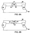
- the sacrificial gate 260 is removed, as by RIE, stopping on the etch stop layer 250 so as to avoid damaging the surface of the substrate 200 below. Thereafter, the etch stop layer 250 is preferably removed, leaving the surface of the substrate 200 exposed in an opening 600 between the spacers 400, as shown in Figure 6A .
- the opening 600 is bound by the top of the substrate 200 and the sidewalls 610 of the spacers 400.
- the polysilicon gate 260 can be removed only and the etch stop layer 250 then left in place as the final gate dielectric. Doing so simplifies processing, as a step of removing the etch stop layer 250 and forming a new gate dielectric 650 are avoided.
- the entire etch stop layer 250 is preferably removed, and the final gate dielectric be formed thereafter on the surface of the substrate 200.
- Post etch cleaning is then preferably conducted following the removal of the etch stop layer 250.
- An advantage of removing the etch stop layer 250 and forming a new layer for use as a gate dielectric 650 is that conditions during formation of the new layer 650 can be optimized for the purpose of providing the final gate dielectric.
- the material and thickness of the final gate dielectric can be more finely controlled.
- a new gate dielectric 650 is formed on the surfaces of the substrate 200, as shown in Figure 6B .
- a gate dielectric 650 having an oxide layer, or alternatively, a nitride layer is thermally grown on the substrate 200 within the opening 600.
- the gate dielectric 650 is formed by deposition, as by low pressure chemical vapor deposition (LPCVD). Other choices of materials exist for the gate dielectric.
- a gate dielectric of hafnium oxide (HfO 2 ) or of zirconium oxide (ZrO 2 ) can be formed as a gate dielectric having a desirably high dielectric constant K, higher than that of either silicon dioxide, silicon nitride or silicon oxynitride.
- K desirably high dielectric constant
- Such high-k gate dielectric may be advantageous for a particular application, such as where a thicker gate dielectric is needed to protect against dielectric breakdown but without sacrificing transistor switching performance.
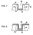
- Figure 7 illustrates a stage in forming the final gate including a metal or conductive metal compound.
- tungsten is used as a preferred material of a first layer 700 in contact with the gate dielectric 650.
- Such choices include but are not limited to: iridium (Ir), niobium (Nb), platinum (Pt), rhenium (Re), rhodium (Rh), ruthenium (Ru), tantalum (Ta), tantalum nitride (TaN), tantalum silicon nitride (TaSiN), tungsten (W), and vanadium (V).
- the metal of the first layer 700 can be selected for its particular compatibility with the gate dielectric 650.
- a first metal layer 700 of hafnium (Hf) can be formed in contact with a gate dielectric 650 of hafnium oxide (HfO 2 ).
- a first metal layer 700 of zirconium (Zr) can be formed in contact with a gate dielectric 650 of zirconium oxide (ZrO 2 ).
- tungsten is a preferred material for use in forming a metal gate.
- tungsten has a workfunction that lies in a middle range between the workfunctions of n-type and p-type semiconductor material. As a result, tungsten can be advantageously used in metal gates of both PFETs and NFETs.
- the first layer 700 of metal is a layer of tungsten.
- a thin layer of tungsten (W) shown at 700 is deposited in the opening 600 in contact with the gate dielectric 650.
- the gate dielectric will be referenced with the number 750 irrespective of whether it is a newly formed gate dielectric 650 or is reused as an appropriate dielectric layer after its earlier use as an etch stop layer 250.
- the first metal layer 700 of tungsten is deposited preferably by a chemical vapor deposition (CVD) technique using a carbonyl of tungsten, preferably W(CO) 6 , as a precursor gas.
- the layer of tungsten shown at 700 is kept thin for best results.
- the thickness of the tungsten layer 700 is deposited to a thickness in the range of 2 to 20 nm and preferably 2 to 10 nm thick.
- the layer of tungsten 700 is a layer covering the substrate and at least part of the spacer sidewall 610.
- the tungsten layer is deposited to coat the entire sidewall(s) of the spacers 610 in the opening 600 and overlying the oxide layer 750.
- Figure 8 illustrates a subsequent processing stage in the formation of the metal gate.
- a diffusion barrier layer is deposited in the opening 600 to coat the thin layer of tungsten 700.
- the diffusion barrier layer can include one or more materials such as titanium nitride (TiN), hafnium nitride (HfN) and zirconium nitride (ZrN). Each of these compounds can be used as a diffusion barrier layer with a variety of different metals formed as a first metal layer 700 in contact with the gate dielectric 650. Diffusion barrier layers including hafnium nitride or zirconium nitride are most preferably used when the first metal layer includes hafnium or zirconium, respectively.
- the diffusion barrier layer 800 includes titanium nitride and will be referred to as a titanium nitride layer 800 or TiN layer 800.
- the diffusion barrier layer preferably includes a thin layer of titanium deposited in contact with the tungsten, followed by a layer of titanium nitride (TiN), as shown at 800.
- This thin layer of titanium is referenced to also as adhesion material or adhesion layer.
- a variety of processes may be employed to form the diffusion barrier layer 800.
- CVD chemical vapor deposition
- the diffusion barrier layer 800 can be deposited using atomic layer deposition (ALD) and physical vapor deposition (PVD) techniques.
- the formation of the diffusion barrier layer 800 by deposition of titanium nitride is preferably followed by annealing to improve the properties of the diffusion barrier layer.
- Annealing is performed to densify the deposited titanium nitride layer 800. It is preferable to conduct the annealing process at lower temperatures so as not to damage the layers of the metal gate.
- the temperature is kept in the range of 400 to 600 degrees Celsius.
- the annealing process is conducted using an H 2 /N 2 mixture at 400 to 600°C for a period of thirty minutes.
- the next processing step after the deposition and optional annealing of the TiN layer 800 is the deposition of a second layer of metal 900 over the TiN layer.
- a second layer of metal or metal compound can be selected from a variety of metals and metal compounds because the diffusion barrier layer 800 prevents reaction between the material of the first layer 700 and the material of the second layer 900.
- the second layer 900 includes a metal or metal compound which is selected for ease of deposition process and conformal properties.
- the second layer 900 includes tungsten.
- the process of depositing the second layer 900 is illustrated in Figure 9 in which a layer of tungsten is deposited as the second layer 900.
- the second layer 900 can be deposited using a CVD process that uses WF 6 as the deposition precursor or source gas.
- WF 6 as the deposition precursor or source gas.
- the deposition of WF 6 is in a downward direction as shown at 900.
- the direction of tungsten growth is indicated by 910 and is upwards and sideways in the opening 600 along the sidewalls 920 of the opening.
- the deposition of the diffusion barrier layer 800 between the first layer 700 and second layer 900 of metal provides several advantages. For one, most diffusion barrier layers such as TiN provide good surface nucleation along the sidewalls 920, as shown in Figure 9 . Improved surface nucleation improves adhesion of tungsten, especially in instances where CVD process is performed using WF 6 as a precursor or a source gas. Improved surface nucleation and improved tungsten adhesion can help reduce peeling of tungsten, a problem often associated with the prior art methodology currently in practice.
- TiN and other diffusion barrier layers have more conformal properties which avoid the problems caused by the non-conformal nature of a tungsten layer deposited from a W(CO) 6 precursor. This particularly addresses the problems of pinch-off and formation of a void in the middle of the gate that arises during deposition of tungsten from a W(CO) 6 precursor. This is due to the fact that the tungsten deposition from the WF 6 precursor fills the opening more conformally, from the sidewalls 910 of the opening rather than from other directions.
- TiN and other diffusion barrier layers are a barrier to fluorine penetration. Since a gas such as WF 6 is used for the deposition of the tungsten gate, and fluorine can damage the underlying silicon, the TiN layer and other diffusion barrier layers can reduce the chance of penetration through a gate oxide layer. This allows a very thin layer of tungsten (preferably between 2-20 nm) to be used initially which greatly reduces the processing cost.
- Figure 10 is an illustration of the resultant metal gate 1000 formed in a preferred embodiment of the invention of the method according to claim 1.
- the resultant metal gate 1000 includes a first layer of metal or metal compound 700 in contact with the gate dielectric 650, a diffusion barrier layer 800 such as the preferred structure of titanium-TiN here and an overlying layer 900 of metal, such as tungsten.
- the metal gate includes tungsten as the first and third layers 700, 900, it operates much like a gate formed entirely of tungsten but without some of the problems that plague the fabrication and performance of a gate formed entirely of tungsten.
- the metal gate 1000 can be planarized using a chemical-mechanical polishing process and stopping on the dielectric layer 500. Gate contacts (not shown) can then be provided to the metal gate structure 1000 from above for interconnection to other elements of the chip.
- the metal gate formed according to the embodiment of the method according to claim 1 illustrated in Figure 10 addresses problems associated with prior art metal gate processes such as structurally deficient gates, gates having voids and gates susceptible to peeling. The scope of the invention is limited only by the claims appended below.
- the metal gate structure fabricated according to the method of the present invention is useful in high performance devices such as semiconductor integrated circuits comprising transistors.
Abstract
Description
- The invention relates to a semiconductor processing method, and more particularly to an improved method for a metal gate structure of a high performance device.
- In the semiconductor fabrication industry, transistors have typically been formed utilizing polysilicon gate electrodes. Polysilicon has been preferred because of its thermal robustness and other special characteristics. An important feature of polysilicon gates is that they can withstand the processing of other elements of transistors such as source and drain regions, during dopant drive-in or other high temperature processes such as annealing processes.
- However, as used in transistors, polysilicon gates are less advantages than metal gates. A polysilicon gate is subject to the formation of a depletion region in operation in which charge carriers are depleted from the polysilicon material above the gate dielectric. This varies from a metal electrode in which charge carriers remain plentiful throughout the electrode. The depletion region has the effect of making the gate dielectric appear thicker in operation than it actually is, such that more charge is needed to turn on the transistor having the polysilicon gate than the transistor having the metal gate. Another disadvantage of polysilicon gates is its incompatibility with high-k dielectric materials. Moreover, polysilicon, even when highly doped to dopant concentrations up to 1020cm-3, is not nearly as good a conductor as metal. This causes polysilicon gates to operate at a slower speed than metal gates. For these reasons, as design requirements demand better performance, metal gates are favored.
- The alternative to using polysilicon gates is fabrication and use of metal gates instead. Metals are much better conductors of electricity, resulting in reduced gate contact resistance, which provides faster device performance. Manufacturing of metal gates, however, can pose serious challenges. For one, metal gates are not thermally robust like polysilicon and therefore cannot be exposed to high temperatures during processing of transistors or other elements of integrated circuits (ICs). Furthermore, metal gates cannot withstand the oxidation ambient necessary to form polysilicon transistor gates. In addition, patterning accuracy required in gate formation is reduced when performing photolithography or other similar techniques on metal surfaces. The reason for this is that photolithography is better achieved on planar surfaces not easily obtainable in metals.
- In recent years, there has been an effort to overcome the limitations of metal gate processing and the operational deficiencies of polysilicon gates through a process of forming transistor structures initially having polysilicon gates which are better able to withstand the initially more severe processing conditions. Thereafter, in later stages of processing when processing conditions are less severe, the polysilicon gates are removed from the structures and replaced with metal gates. By this replacement gate process, the initial severe process conditions need not be modified, and the photolithography benefits associated with polysilicon processing are preserved. The initial use of polysilicon gates also takes advantage of the ability of polysilicon to block ion-implantation to the channel region of the transistor when performing source and drain implants to the transistor. As an example,
US 2003/143825 A1 (Matsuo, Kouji, et el. "Semiconductor Device and Method of Manufacturing the Same") describes a semiconductor device, and methods of manufacturing such a device, that utilises polysilicon as an initial dummy gates prior to formation of metal gates. - In a replacement gate fabrication approach, a polysilicon gate is formed over an etch stop layer in contact with a single-crystal semiconductor region of a substrate, a pair of spacers being disposed on sidewalls of the gate. The etch stop layer is typically a thin layer of silicon dioxide which is grown thermally on the surface of the substrate in an oxygen ambient. In such case, the etch stop layer can be referred to as a sacrificial gate oxide layer. Later, the polysilicon material is removed from between the pair of spacers, as by an anisotropic vertical etch process such as a reactive ion etch (RIE) stopping on the etch stop layer. The etch stop layer is then cleared from the surface of the substrate as by a dry etch or an isotropic wet etch selective to the material of the sidewall spacers. This creates an opening between the spacers where a gate dielectric, usually a thermally grown oxide, is then formed. Thereafter, a metal gate is formed in the opening between the spacers contacting the gate dielectric underneath.
- A preferred metal for forming such metal gates is tungsten (W). Tungsten is usually deposited using a chemical vapor deposition step (CVD) where a deposition precursor including a (source) gas such as WF6 is used. A particular challenge arises in the deposition of tungsten, however, especially when using WF6 as the deposition precursor. Fluorine radicals in the WF6 gas can be harmful both to oxide and silicon substances. Consequently, the fluorine gas can attack gate oxide and the silicon below the gate oxide. A different gas such as W(CO)6 may alternatively be used but the non-conformal properties of W(CO)6 can cause the formation of a defective tungsten gate.
Figure 1 illustrates the non-conformal tungsten properties of deposition using a W(CO)6 gas, leading to the pinch-off of the opening and a defective tungsten gate formation. - In
Figure 1 , W(CO)6 110 has been deposited to coat the gate opening 100. The spacers are shown at 105. As illustrated in 115, the non-conformal characteristics of W(CO)6, especially when deposited in thick layers of 10 nm or more, create a pinchoff at the top of the gate opening 100. In addition, the non-conformal property of such deposition causes tungsten to accumulate unevenly so that a void is created in the middle or center of the tungsten gate, rendering the gate structurally defective. The pinchoff problem is extremely challenging in high performance environments where the width of the opening is narrow. - Another challenge, when using either WF6 or W·(CO)6 gases, is that effective deposition of tungsten requires a good nucleation site to be present on the surfaces (i.e. sidewalls) where it is being deposited. The presence of oxides, especially on surfaces, affect the ability of tungsten to be deposited and to adhere properly to the surfaces it is being deposited on. Ineffective deposition of tungsten can lead to structurally defective gates in which the gate conductor material may peel or pop off from their adjacent surfaces.
- An improved method is therefore required that enables the formation of metal gates, particularly those including tungsten as the predominant metal that addresses the processing challenges faced in the above-described processing methods.
- The invention provides a method for a metal replacement gate of a high performance device as defined in claim 1.
- According to a preferred aspect of the invention, chemical mechanical polishing is used to remove deposited metal overlying the dielectric layer outside of the opening.
- Embodiments of the invention are described below in more detail, by way of example, with reference to the accompanying drawings in which:
-
Figure 1 is an illustration of a potential pinchoff problem caused by deposition of a thick layer of tungsten in an opening; -
Figure 2A though 5 illustrate initial processing steps in the formation of a sacrificial gate structure of the method of the present invention; -
Figure 6A is a cross sectional view of a substrate with spacers formed on its surface subsequent to the removal of a sacrificial gate structure; -
Figure 6B illustrates an alternate embodiment of the method of the present invention where a new layer of gate oxide is deposited after the removal of sacrificial gate structure; and -
Figures 7 though 10 are subsequent steps in the formation of a metal gate structure of the method of the present invention. - The present invention particularly addresses and solves problems related to the formation of metal gates in transistors. In an embodiment of the method of the invention, the metal can be selected for workfunction compatibility with the conductivity type of transistor in which it is used. For example, in an NFET, a metal gate having a workfunction equivalent to that of n-type conductivity semiconductor material performs better than a metal having a mid-range workfunction or a workfunction equivalent to that of p-type semiconductor material. In an embodiment of the invention, a method according to claim 1 is provided by which a metal having a desirable workfunction can be formed in contact with the gate dielectric in an integrated structure and method that decouples the particular choice of metal used in that step from later processing.
- In an embodiment of the method according to claim 1 described herein, the particular metal formed in contact with the gate can be selected for its compatibility with the gate dielectric material. For example, the gate dielectric can include a material specially selected for its high dielectric constant K such as hafnium oxide (HfO2) or zirconium oxide (ZrO2). The gate can then include a metal in contact with the gate dielectric that has superior compatibility, such as hafnium (Hf) or zirconium (Zr).
- In another embodiment of the invention of the method according to claim 1 a first layer of metal is formed in contact with the gate dielectric. Such layer is desirably selected for its properties in terms of workfunction, compatibility with the gate dielectric, or characteristics of the process in depositing the metal on the gate dielectric. A diffusion barrier layer is then formed over the first layer of metal. Thereafter, a second layer of metal is formed over the diffusion barrier layer. Because of the presence of the diffusion barrier layer, a greater choice is available over the metal used in the second layer of metal. Thus, for example, that metal can be selected for the characteristics of the deposition process used to form the second layer.
- A structure and process is provided for forming metal gates having tungsten (W) as a preferred material of a first layer in contact with the gate dielectric. Tungsten (W) is a particularly versatile material for metal gates because it has a workfunction at about the middle of the difference between the workfunctions of n-type and p-type semiconductor materials. Because of that, tungsten can be used in metal gates of n-type field effect transistors (NFETs) in which electrons are the dominant charge carriers and also p-type field effect transistors (PFETs) in which holes are the dominant charge carrier. Moreover, unlike some other metals which can only be deposited by physical vapor deposition (PVD), e.g. sputtering, tungsten can be deposited using a chemical vapor deposition (CVD) process.
- In a particular embodiment of the method according to claim 1, problems of forming metal gates in openings having a large ratio of height to width, i.e. openings having "high aspect ratio", are addressed. The embodiment of the present invention of the method according to claim 1 allows particular deposition processes to be selected for their particular advantages, despite other problems that are associated with those processes. For example, a relatively thin layer of metal can be formed as a first layer of metal by a deposition process that is compatible with the gate dielectric. However, that deposition process can be problematic if attempts are made to use it to form the entire gate. As described above, deposition of tungsten from a carbonyl of tungsten (W(CO)6) is such a deposition process that is compatible with oxide gate dielectrics such as silicon dioxide, but with which filling problems including pinch-off and voids have been observed in high aspect ratio openings.
-
Figure 2A illustrates asemiconductor substrate 200. The term "substrate" is used herein for ease of reference and includes a variety of types of substrates including bulk semiconductor substrates, semiconductor-on-insulator substrates such as a "silicon-on-insulator" (SOI) substrates, germanium (Ge) substrates and silicon germanium (SiGe) substrates. Such substrates include a region of a single-crystal semiconductor at a main surface thereof. The term substrate may also be applied to a substrate having a thin deposited semiconductor layer when the process described herein is used to form a thin film transistor (TFT). - Isolation structures as shown at 220 are then formed on the
substrate 200. In the embodiment of the method according to claim 1 illustrated inFigure 2A , theisolation structures 220 are raised, however, there is no need for these structures to be raised and other embodiments of the method according to claim 1 can be achieved where the structures are planarized with the substrate. Furthermore, theisolation structures 220 can include a variety of structures such as shallow trench isolation and are formed selectively on thesubstrate 200. - The area of the substrate defined by and in between the
isolation structures 220 is known as the active area and is shown in Figure 2 at 240. Theactive area 240 will house the active electrical devices. The purpose of the isolation structures is to provide electrical isolation between devices in various and particularly adjacentactive areas 240. -
Figure 2B illustrates a next processing stage where initial process steps are taken to form a sacrificial polysilicon gate on thesubstrate 200. As shown inFigure 2B , anetch stop layer 250 is formed by deposition or grow on thesubstrate 200. In a preferred embodiment of the present invention of the method according to claim 1 as illustrated inFigure 2B , theetch stop layer 250 includes a layer of oxide such as silicon dioxide when thesubstrate 200 consists essentially of silicon. In such case, theetch stop layer 250 can be referred to as a sacrificial gate oxide layer or a sacrificial oxide layer. Alternatively, a nitride such as silicon nitride, silicon oxynitride or another material can be used for theetch stop layer 250. Theetch stop layer 250 is preferably an oxide layer. As shown inFigure 2B , alayer 260 of polysilicon is then deposited as a sacrificial gate material on theetch stop layer 250. As shown inFigure 3 , thesacrificial gate material 260 andetch stop layer 250 are then patterned together. Since the sacrificial gate is formed of polysilicon as is widely used in NFET and PFET transistors, patterning processes are readily available. - In the embodiment provided in
Figure 3 , photolithography is used to pattern agate stack structure 300 including an etch step layer provided as anoxide layer 250 and the polysilicon layer thereon 260. The photolithography procedure is then followed by an anisotropic etch process such as reactive ion etch (RIE) but other methods could be used instead. - In the next processing step, spacers are formed on the sidewalls of the
gate stack structure 300 as shown inFigure 4 . In an embodiment of the method according to claim 1, thespacers 400 are formed by deposition of a conformal spacer material followed by an anisotropic vertical etch such as RIE such that only the vertically-oriented spacers remain thereafter, as adhering to sidewalls of thesacrificial gate 300. The material of which spacers 400 are formed can include one or more materials from a variety of available materials selected for integration in the particular process steps that are used. For example, when theetch stop layer 250 includes an oxide, thespacers 400 are preferably formed of a non-oxide material such as silicon nitride or other nitride such that in a later process step in which the etch stop is removed by isotropic wet etching, etch selectivity is provided between the non-oxide spacers and the oxideetch stop layer 250. Alternatively, when theetch stop layer 250 is formed of a nitride such as silicon nitride, thespacers 400 are desirably formed of a non-nitride material to provide etch selectivity between the non-nitride spacers and the nitrideetch stop layer 250. When theetch stop layer 250 is formed of silicon oxynitride,spacers 400 can be formed of either oxide or nitride as an isotropic wet etch chemistry having etch selectivity to either oxide or nitride. - In addition,
Figure 4 illustrates a process of forming the source and drain regions as shown at 410 and 420. Since a sacrificial gate of polysilicon is used, thesubstrate 200 can also be doped to form the source and drainregions 410 and 420 in theactive area 240. The doping involves the implantation of ions into the substrate to alter the conductivity of the source and drainregions 410 and 420. Polysilicon, as mentioned above, has the ability to block such implantation to the channel region, shown at 450 inFigure 4 . - The regions shown at 410 and 420 in
Figure 4 can also be implanted to form lightly doped source/drain extension regions and/or halo implanted. In addition, either or both n-type and p-type impurities can be implanted as required in order to form the specific desired components. For example, if circuits are to implemented in a complementary metal oxide semiconductor (CMOS) technology, n-type and p-type dopants must be implanted into respective portions of the substrate to form the source and drain regions of the p-type or n-type transistors in that technology. Polysilicon has an ability to block the ion implantation of doped atoms, therefore, thesacrificial polysilicon gate 300 and thespacers 400 together function as an implant mask. - The use of a sacrificial polysilicon gate in these early stages of processing a metal gate allows high temperature processing to be performed. For example, a high temperature dopant drive-in process is generally required following implanting a dopant into source and drain regions of the substrate after patterning the gate.
- Next, as shown in
Figure 5 , aninterlevel dielectric 500 layer is blanket deposited over thesubstrate 200. In an embodiment of the method according to claim 1 theinterlevel dielectric 500 is then planarized, stopping at thesacrificial gate stack 300. A variety of processes are available for planarization such as chemical mechanical polishing. - In
Figure 6A , thesacrificial gate 260 is removed, as by RIE, stopping on theetch stop layer 250 so as to avoid damaging the surface of thesubstrate 200 below. Thereafter, theetch stop layer 250 is preferably removed, leaving the surface of thesubstrate 200 exposed in anopening 600 between thespacers 400, as shown inFigure 6A . Theopening 600 is bound by the top of thesubstrate 200 and thesidewalls 610 of thespacers 400. - In an alternative embodiment, when the
etch stop layer 250 is formed of a material and thickness suitable to perform as a gate dielectric, thepolysilicon gate 260 can be removed only and theetch stop layer 250 then left in place as the final gate dielectric. Doing so simplifies processing, as a step of removing theetch stop layer 250 and forming anew gate dielectric 650 are avoided. - However, because of the possibility of damage to the
etch stop layer 250 during the removal of thesacrificial polysilicon gate 260, especially when the sacrificial gate is removed by RIE, the entireetch stop layer 250 is preferably removed, and the final gate dielectric be formed thereafter on the surface of thesubstrate 200. Post etch cleaning is then preferably conducted following the removal of theetch stop layer 250. - An advantage of removing the
etch stop layer 250 and forming a new layer for use as agate dielectric 650 is that conditions during formation of thenew layer 650 can be optimized for the purpose of providing the final gate dielectric. Thus, in such embodiment of the method according to claim 1, the material and thickness of the final gate dielectric can be more finely controlled. - In an embodiment in which the
etch stop layer 250 is removed, anew gate dielectric 650 is formed on the surfaces of thesubstrate 200, as shown inFigure 6B . In a preferred embodiment of the method according to claim 1, agate dielectric 650 having an oxide layer, or alternatively, a nitride layer, is thermally grown on thesubstrate 200 within theopening 600. In another embodiment, thegate dielectric 650 is formed by deposition, as by low pressure chemical vapor deposition (LPCVD). Other choices of materials exist for the gate dielectric. For example, a gate dielectric of hafnium oxide (HfO2) or of zirconium oxide (ZrO2) can be formed as a gate dielectric having a desirably high dielectric constant K, higher than that of either silicon dioxide, silicon nitride or silicon oxynitride. Such high-k gate dielectric may be advantageous for a particular application, such as where a thicker gate dielectric is needed to protect against dielectric breakdown but without sacrificing transistor switching performance. - Once the
final gate dielectric 650 has been formed, the final gate can then be formed.Figure 7 illustrates a stage in forming the final gate including a metal or conductive metal compound. In the exemplary embodiment of the method according to claim 1 illustrated inFigures 7 to 10 , tungsten is used as a preferred material of afirst layer 700 in contact with thegate dielectric 650. A range of choices exist for metals and metal compounds which can be deposited onto thegate dielectric 650 as afirst metal layer 700 of the gate. Such choices include but are not limited to: iridium (Ir), niobium (Nb), platinum (Pt), rhenium (Re), rhodium (Rh), ruthenium (Ru), tantalum (Ta), tantalum nitride (TaN), tantalum silicon nitride (TaSiN), tungsten (W), and vanadium (V). - In addition, when the gate dielectric is formed of a particular material, for example, a high-K dielectric material such as hafnium oxide (HfO) or zirconium oxide (zero), the metal of the
first layer 700 can be selected for its particular compatibility with thegate dielectric 650. For example, afirst metal layer 700 of hafnium (Hf) can be formed in contact with agate dielectric 650 of hafnium oxide (HfO2). Similarly, afirst metal layer 700 of zirconium (Zr) can be formed in contact with agate dielectric 650 of zirconium oxide (ZrO2). - For many of these metals and metal compounds, only physical vapor deposition processes, e.g. sputtering, exist at the present time. However, chemical vapor deposition processes do exist for depositing tungsten. Therefore, tungsten is a preferred material for use in forming a metal gate. Moreover, tungsten has a workfunction that lies in a middle range between the workfunctions of n-type and p-type semiconductor material. As a result, tungsten can be advantageously used in metal gates of both PFETs and NFETs.
- A preferred embodiment of the method according to claim 1 for forming a metal gate will now be described in which the
first layer 700 of metal is a layer of tungsten. As shown inFigure 7 , a thin layer of tungsten (W) shown at 700 is deposited in theopening 600 in contact with thegate dielectric 650. For ease of reference, the gate dielectric will be referenced with thenumber 750 irrespective of whether it is a newly formedgate dielectric 650 or is reused as an appropriate dielectric layer after its earlier use as anetch stop layer 250. - The
first metal layer 700 of tungsten is deposited preferably by a chemical vapor deposition (CVD) technique using a carbonyl of tungsten, preferably W(CO)6, as a precursor gas. The layer of tungsten shown at 700 is kept thin for best results. In a preferred embodiment of the present invention of the method according to claim 1 the thickness of thetungsten layer 700 is deposited to a thickness in the range of 2 to 20 nm and preferably 2 to 10 nm thick. The layer oftungsten 700 is a layer covering the substrate and at least part of thespacer sidewall 610. In an embodiment of the present invention of the method according to claim 1 as shown inFigure 7 , the tungsten layer is deposited to coat the entire sidewall(s) of thespacers 610 in theopening 600 and overlying theoxide layer 750. -
Figure 8 illustrates a subsequent processing stage in the formation of the metal gate. InFigure 8 , a diffusion barrier layer is deposited in theopening 600 to coat the thin layer oftungsten 700. The diffusion barrier layer can include one or more materials such as titanium nitride (TiN), hafnium nitride (HfN) and zirconium nitride (ZrN). Each of these compounds can be used as a diffusion barrier layer with a variety of different metals formed as afirst metal layer 700 in contact with thegate dielectric 650. Diffusion barrier layers including hafnium nitride or zirconium nitride are most preferably used when the first metal layer includes hafnium or zirconium, respectively. In the preferred embodiment of the method according to claim 1 described as follows, thediffusion barrier layer 800 includes titanium nitride and will be referred to as atitanium nitride layer 800 orTiN layer 800. - In a preferred embodiment of the method according to claim 1 in which the first layer of
metal 700 is formed of tungsten, the diffusion barrier layer preferably includes a thin layer of titanium deposited in contact with the tungsten, followed by a layer of titanium nitride (TiN), as shown at 800. This thin layer of titanium is referenced to also as adhesion material or adhesion layer. A variety of processes may be employed to form thediffusion barrier layer 800. In a preferred embodiment of the method according to claim 1, chemical vapor deposition (CVD) is used. Alternatively, thediffusion barrier layer 800 can be deposited using atomic layer deposition (ALD) and physical vapor deposition (PVD) techniques. - The formation of the
diffusion barrier layer 800 by deposition of titanium nitride is preferably followed by annealing to improve the properties of the diffusion barrier layer. Annealing is performed to densify the depositedtitanium nitride layer 800. It is preferable to conduct the annealing process at lower temperatures so as not to damage the layers of the metal gate. In an embodiment of the method according to claim 1 in which an annealing process is conducted, the temperature is kept in the range of 400 to 600 degrees Celsius. In a preferred embodiment, the annealing process is conducted using an H2/N2 mixture at 400 to 600°C for a period of thirty minutes. - In a preferred embodiment of the method according to claim 1, the next processing step after the deposition and optional annealing of the
TiN layer 800 is the deposition of a second layer ofmetal 900 over the TiN layer. With thediffusion barrier layer 800 in place, a second layer of metal or metal compound can be selected from a variety of metals and metal compounds because thediffusion barrier layer 800 prevents reaction between the material of thefirst layer 700 and the material of thesecond layer 900. Preferably, thesecond layer 900 includes a metal or metal compound which is selected for ease of deposition process and conformal properties. Preferably, thesecond layer 900 includes tungsten. - The process of depositing the
second layer 900 is illustrated inFigure 9 in which a layer of tungsten is deposited as thesecond layer 900. In an embodiment of the method according to claim 1, thesecond layer 900 can be deposited using a CVD process that uses WF6 as the deposition precursor or source gas. As illustrated in the example ofFigure 9 , the deposition of WF6 is in a downward direction as shown at 900. The direction of tungsten growth is indicated by 910 and is upwards and sideways in theopening 600 along thesidewalls 920 of the opening. - The deposition of the
diffusion barrier layer 800 between thefirst layer 700 andsecond layer 900 of metal provides several advantages. For one, most diffusion barrier layers such as TiN provide good surface nucleation along thesidewalls 920, as shown inFigure 9 . Improved surface nucleation improves adhesion of tungsten, especially in instances where CVD process is performed using WF6 as a precursor or a source gas. Improved surface nucleation and improved tungsten adhesion can help reduce peeling of tungsten, a problem often associated with the prior art methodology currently in practice. - In addition, TiN and other diffusion barrier layers have more conformal properties which avoid the problems caused by the non-conformal nature of a tungsten layer deposited from a W(CO) 6 precursor. This particularly addresses the problems of pinch-off and formation of a void in the middle of the gate that arises during deposition of tungsten from a W(CO)6precursor. This is due to the fact that the tungsten deposition from the WF6 precursor fills the opening more conformally, from the
sidewalls 910 of the opening rather than from other directions. - In addition TiN and other diffusion barrier layers are a barrier to fluorine penetration. Since a gas such as WF6 is used for the deposition of the tungsten gate, and fluorine can damage the underlying silicon, the TiN layer and other diffusion barrier layers can reduce the chance of penetration through a gate oxide layer. This allows a very thin layer of tungsten (preferably between 2-20 nm) to be used initially which greatly reduces the processing cost.
-
Figure 10 is an illustration of theresultant metal gate 1000 formed in a preferred embodiment of the invention of the method according to claim 1. As shown inFigure 10 , theresultant metal gate 1000 includes a first layer of metal ormetal compound 700 in contact with thegate dielectric 650, adiffusion barrier layer 800 such as the preferred structure of titanium-TiN here and anoverlying layer 900 of metal, such as tungsten. When the metal gate includes tungsten as the first andthird layers - The
metal gate 1000 can be planarized using a chemical-mechanical polishing process and stopping on thedielectric layer 500. Gate contacts (not shown) can then be provided to themetal gate structure 1000 from above for interconnection to other elements of the chip. The metal gate formed according to the embodiment of the method according to claim 1 illustrated inFigure 10 addresses problems associated with prior art metal gate processes such as structurally deficient gates, gates having voids and gates susceptible to peeling. The scope of the invention is limited only by the claims appended below. - The metal gate structure fabricated according to the method of the present invention is useful in high performance devices such as semiconductor integrated circuits comprising transistors.
Claims (12)
- A method of making a metal gate structure (1000) in a transistor, comprising:forming an etch stop layer (250) on a semiconductor region of a substrate (240);forming a sacrificial gate (260) on said etch stop layer (250), thereby forming a sacrificial gate structure (300);providing a pair of dielectric spacers (400) on sidewalls of said sacrificial gate structure (300);forming a dielectric layer (500) on said substrate (240) having a top surface generally planar to a top of said sacrificial gate (260);removing said sacrificial gate (260) to form an opening (600) between said spacers (400);removing said etch stop layer (250) from a bottom of said opening (600);forming a gate dielectric (750) on said semiconductor region in said opening (600);depositing a first layer (700) of at least one of metal and metal compound in said opening (600), contacting said gate dielectric (750) and sidewalls of said spacers (400);forming a diffusion barrier layer (800) on said first layer (700) in said opening (600);depositing a second layer (900) of at least one of metal and metal compound on said diffusion barrier layer (800) in said opening (600); and,said first layer (700) is deposited from a carbonyl containing precursor and said second layer (900) is deposited from a fluorine containing precursor.
- The method of claim 1 wherein said gate dielectric (750) is formed by thermal growth.
- The method of either of claims 1 or 2 wherein said first layer (700) is deposited from a W(CO)6 precursor and said second layer (900) is deposited from a WF6 precursor.
- The method of any of the above claims wherein said sacrificial gate (260) includes polysilicon.
- The method of any of the above claims further comprising depositing a layer of adhesion material prior to forming said diffusion barrier layer (800).
- The method of any of the above claims wherein said first layer (700) consists essentially of at least one material selected from the group consisting of iridium (Ir), niobium (Nb) , platinum (Pt), rhenium (Re), rhodium (Rh), ruthenium (Ru), tantalum (Ta), tantalum nitride (TaN), tantalum silicon nitride (TaSiN), tungsten (W), and vanadium (V).
- The method of claim 6 wherein said second layer (900) consists essentially of at least one material selected from the group consisting of iridium (Ir), niobium (Nb), platinum (Pt), rhenium (Re), rhodium (Rh), ruthenium (Ru), tantalum (Ta), tantalum nitride (TaN), tantalum silicon nitride (TaSiN), tungsten (W), vanadium (V), Ni silicide, Co silicide and Ti silicide.
- The method of any of the above claims wherein said diffusion barrier layer (800) includes at least one of a nitride of titanium, a nitride of hafnium and a nitride of zirconium.
- The method of any of the above claims wherein said gate dielectric (750) consists essentially of an oxide.
- The method of any of the above claims wherein said substrate (240) is selected from the group consisting of a bulk semiconductor substrate, semiconductor-on-insulator substrate, silicon-on-insulator substrate, silicon-germanium substrate, and germanium substrate.
- The method of any of the above claims wherein said semiconductor region includes at least one selected from the group consisting of polycrystalline silicon and amorphous silicon.
- The method of any of the above claims wherein said dielectric spacers (400) include at least one material selected from the group consisting of silicon oxide, silicon oxynitride, silicon nitride, metal oxide, silicates and mixtures of said materials.
Applications Claiming Priority (2)
| Application Number | Priority Date | Filing Date | Title |
|---|---|---|---|
| US10/605,106 US6921711B2 (en) | 2003-09-09 | 2003-09-09 | Method for forming metal replacement gate of high performance |
| PCT/US2004/027327 WO2005024906A2 (en) | 2003-09-09 | 2004-08-20 | Structure and method for metal replacement gate of high performance device |
Publications (3)
| Publication Number | Publication Date |
|---|---|
| EP1668706A2 EP1668706A2 (en) | 2006-06-14 |
| EP1668706A4 EP1668706A4 (en) | 2008-11-05 |
| EP1668706B1 true EP1668706B1 (en) | 2009-08-05 |
Family
ID=34225869
Family Applications (1)
| Application Number | Title | Priority Date | Filing Date |
|---|---|---|---|
| EP04786558A Not-in-force EP1668706B1 (en) | 2003-09-09 | 2004-08-20 | Method for metal replacement gate of high performance device |
Country Status (8)
| Country | Link |
|---|---|
| US (1) | US6921711B2 (en) |
| EP (1) | EP1668706B1 (en) |
| JP (1) | JP4629674B2 (en) |
| KR (1) | KR100791433B1 (en) |
| CN (1) | CN1846313B (en) |
| AT (1) | ATE438928T1 (en) |
| DE (1) | DE602004022435D1 (en) |
| WO (1) | WO2005024906A2 (en) |
Families Citing this family (341)
| Publication number | Priority date | Publication date | Assignee | Title |
|---|---|---|---|---|
| JP2004296491A (en) * | 2003-03-25 | 2004-10-21 | Sanyo Electric Co Ltd | Semiconductor device |
| US7276408B2 (en) * | 2003-10-08 | 2007-10-02 | Texas Instruments Incorporated | Reduction of dopant loss in a gate structure |
| US20050151166A1 (en) * | 2004-01-09 | 2005-07-14 | Chun-Chieh Lin | Metal contact structure and method of manufacture |
| US7390709B2 (en) * | 2004-09-08 | 2008-06-24 | Intel Corporation | Method for making a semiconductor device having a high-k gate dielectric layer and a metal gate electrode |
| US7189431B2 (en) * | 2004-09-30 | 2007-03-13 | Tokyo Electron Limited | Method for forming a passivated metal layer |
| US7598545B2 (en) * | 2005-04-21 | 2009-10-06 | International Business Machines Corporation | Using metal/metal nitride bilayers as gate electrodes in self-aligned aggressively scaled CMOS devices |
| US7224630B2 (en) * | 2005-06-24 | 2007-05-29 | Freescale Semiconductor, Inc. | Antifuse circuit |
| US7195999B2 (en) * | 2005-07-07 | 2007-03-27 | Micron Technology, Inc. | Metal-substituted transistor gates |
| US20070045752A1 (en) * | 2005-08-31 | 2007-03-01 | Leonard Forbes | Self aligned metal gates on high-K dielectrics |
| US7867845B2 (en) | 2005-09-01 | 2011-01-11 | Micron Technology, Inc. | Transistor gate forming methods and transistor structures |
| US8053849B2 (en) * | 2005-11-09 | 2011-11-08 | Advanced Micro Devices, Inc. | Replacement metal gate transistors with reduced gate oxide leakage |
| US7663237B2 (en) * | 2005-12-27 | 2010-02-16 | Taiwan Semiconductor Manufacturing Company, Ltd. | Butted contact structure |
| US7425497B2 (en) | 2006-01-20 | 2008-09-16 | International Business Machines Corporation | Introduction of metal impurity to change workfunction of conductive electrodes |
| US7709402B2 (en) | 2006-02-16 | 2010-05-04 | Micron Technology, Inc. | Conductive layers for hafnium silicon oxynitride films |
| JP4492589B2 (en) * | 2006-06-20 | 2010-06-30 | ソニー株式会社 | Manufacturing method of semiconductor device |
| KR100843879B1 (en) * | 2007-03-15 | 2008-07-03 | 주식회사 하이닉스반도체 | Semiconductor device and method for fabricating the same |
| US20080230906A1 (en) * | 2007-03-22 | 2008-09-25 | Keith Kwong Hon Wong | Contact structure having dielectric spacer and method |
| JP4552973B2 (en) * | 2007-06-08 | 2010-09-29 | セイコーエプソン株式会社 | Manufacturing method of semiconductor device |
| KR100863534B1 (en) * | 2007-06-27 | 2008-10-15 | 주식회사 하이닉스반도체 | Semiconductor device with metal gate and method for fabricating the same |
| US7718514B2 (en) * | 2007-06-28 | 2010-05-18 | International Business Machines Corporation | Method of forming a guard ring or contact to an SOI substrate |
| US7906390B2 (en) * | 2007-07-20 | 2011-03-15 | International Business Machines Corporation | Thin gate electrode CMOS devices and methods of fabricating same |
| US7795097B2 (en) * | 2007-11-20 | 2010-09-14 | Texas Instruments Incorporated | Semiconductor device manufactured by removing sidewalls during replacement gate integration scheme |
| US7955964B2 (en) | 2008-05-14 | 2011-06-07 | Taiwan Semiconductor Manufacturing Company, Ltd. | Dishing-free gap-filling with multiple CMPs |
| US7800166B2 (en) * | 2008-05-30 | 2010-09-21 | Intel Corporation | Recessed channel array transistor (RCAT) structures and method of formation |
| US8048752B2 (en) | 2008-07-24 | 2011-11-01 | Taiwan Semiconductor Manufacturing Company, Ltd. | Spacer shape engineering for void-free gap-filling process |
| US8735235B2 (en) * | 2008-08-20 | 2014-05-27 | Taiwan Semiconductor Manufacturing Company, Ltd. | Integrated circuit metal gate structure and method of fabrication |
| US8030718B2 (en) * | 2008-09-12 | 2011-10-04 | Taiwan Semiconductor Manufacturing Company, Ltd. | Local charge and work function engineering on MOSFET |
| US8093116B2 (en) * | 2008-10-06 | 2012-01-10 | Taiwan Semiconductor Manufacturing Company, Ltd. | Method for N/P patterning in a gate last process |
| US7923321B2 (en) * | 2008-11-03 | 2011-04-12 | Taiwan Semiconductor Manufacturing Company, Ltd. | Method for gap filling in a gate last process |
| US7915105B2 (en) * | 2008-11-06 | 2011-03-29 | Taiwan Semiconductor Manufacturing Company, Ltd. | Method for patterning a metal gate |
| US7691701B1 (en) * | 2009-01-05 | 2010-04-06 | International Business Machines Corporation | Method of forming gate stack and structure thereof |
| US20100314690A1 (en) * | 2009-06-15 | 2010-12-16 | Taiwan Semiconductor Manufacturing Company, Ltd. | Sidewall-Free CESL for Enlarging ILD Gap-Fill Window |
| US8294202B2 (en) * | 2009-07-08 | 2012-10-23 | Taiwan Semiconductor Manufacturing Company, Ltd. | Metal gate structure of a semiconductor device |
| KR101604054B1 (en) * | 2009-09-03 | 2016-03-16 | 삼성전자주식회사 | Semiconductor devices and methods of forming thereof |
| CN102097382B (en) * | 2009-12-15 | 2013-07-24 | 中芯国际集成电路制造(上海)有限公司 | Method for manufacturing semiconductor device |
| US8513107B2 (en) * | 2010-01-26 | 2013-08-20 | Taiwan Semiconductor Manufacturing Co., Ltd. | Replacement gate FinFET devices and methods for forming the same |
| US8564072B2 (en) | 2010-04-02 | 2013-10-22 | Taiwan Semiconductor Manufacturing Company, Ltd. | Semiconductor device having a blocking structure and method of manufacturing the same |
| US8551874B2 (en) | 2010-05-08 | 2013-10-08 | International Business Machines Corporation | MOSFET gate and source/drain contact metallization |
| US8637390B2 (en) * | 2010-06-04 | 2014-01-28 | Applied Materials, Inc. | Metal gate structures and methods for forming thereof |
| CN102299061B (en) * | 2010-06-22 | 2014-05-14 | 中国科学院微电子研究所 | Method for manufacturing semiconductor device |
| CN102299154B (en) * | 2010-06-22 | 2013-06-12 | 中国科学院微电子研究所 | Semiconductor structure and manufacturing method thereof |
| CN102386083B (en) * | 2010-09-02 | 2013-09-11 | 中芯国际集成电路制造(上海)有限公司 | MOS (metal oxide semiconductor) transistor and manufacturing method of MOS transistor gate dielectric layer |
| CN102420136B (en) * | 2010-09-25 | 2013-08-14 | 中芯国际集成电路制造(上海)有限公司 | Forming method of MOS (Metal Oxide Semiconductor) transistor |
| US9006052B2 (en) | 2010-10-11 | 2015-04-14 | International Business Machines Corporation | Self aligned device with enhanced stress and methods of manufacture |
| CN102468145A (en) * | 2010-11-01 | 2012-05-23 | 中芯国际集成电路制造(上海)有限公司 | Method for forming metal grid |
| CN102487012B (en) * | 2010-12-02 | 2014-03-12 | 中芯国际集成电路制造(北京)有限公司 | Manufacturing method of transistor |
| CN102487010B (en) * | 2010-12-02 | 2013-11-06 | 中芯国际集成电路制造(北京)有限公司 | Method for forming metal grid and MOS (Metal Oxide Semiconductor) transistor |
| US8420473B2 (en) | 2010-12-06 | 2013-04-16 | International Business Machines Corporation | Replacement gate devices with barrier metal for simultaneous processing |
| CN102544098B (en) | 2010-12-31 | 2014-10-01 | 中国科学院微电子研究所 | MOS (Metal-Oxide-Semiconductor) transistor and forming method thereof |
| US8574990B2 (en) | 2011-02-24 | 2013-11-05 | United Microelectronics Corp. | Method of manufacturing semiconductor device having metal gate |
| US8802524B2 (en) * | 2011-03-22 | 2014-08-12 | United Microelectronics Corp. | Method of manufacturing semiconductor device having metal gates |
| US8324118B2 (en) | 2011-03-28 | 2012-12-04 | United Microelectronics Corp. | Manufacturing method of metal gate structure |
| US8519454B2 (en) | 2011-03-30 | 2013-08-27 | International Business Machines Corporation | Structure and process for metal fill in replacement metal gate integration |
| US9384962B2 (en) | 2011-04-07 | 2016-07-05 | United Microelectronics Corp. | Oxygen treatment of replacement work-function metals in CMOS transistor gates |
| US20120261770A1 (en) * | 2011-04-14 | 2012-10-18 | Kun-Hsien Lin | Metal gate structure |
| US8530980B2 (en) | 2011-04-27 | 2013-09-10 | United Microelectronics Corp. | Gate stack structure with etch stop layer and manufacturing process thereof |
| CN102810561B (en) | 2011-06-02 | 2015-12-02 | 中芯国际集成电路制造(上海)有限公司 | Semiconductor device and manufacture method thereof |
| US8704294B2 (en) | 2011-06-13 | 2014-04-22 | United Microelectronics Corp. | Semiconductor device having metal gate and manufacturing method thereof |
| US8673758B2 (en) | 2011-06-16 | 2014-03-18 | United Microelectronics Corp. | Structure of metal gate and fabrication method thereof |
| US9490342B2 (en) | 2011-06-16 | 2016-11-08 | United Microelectronics Corp. | Method for fabricating semiconductor device |
| US8536038B2 (en) | 2011-06-21 | 2013-09-17 | United Microelectronics Corp. | Manufacturing method for metal gate using ion implantation |
| US8486790B2 (en) | 2011-07-18 | 2013-07-16 | United Microelectronics Corp. | Manufacturing method for metal gate |
| US20130023129A1 (en) | 2011-07-20 | 2013-01-24 | Asm America, Inc. | Pressure transmitter for a semiconductor processing environment |
| US8569135B2 (en) | 2011-07-20 | 2013-10-29 | International Business Machines Corporation | Replacement gate electrode with planar work function material layers |
| US9755039B2 (en) | 2011-07-28 | 2017-09-05 | Taiwan Semiconductor Manufacturing Company, Ltd. | Semiconductor device having a metal gate electrode stack |
| US8853700B2 (en) | 2011-08-10 | 2014-10-07 | International Business Machines Corporation | Cross-coupling of gate conductor line and active region in semiconductor devices |
| US8962477B2 (en) * | 2011-08-12 | 2015-02-24 | Taiwan Semiconductor Manufacturing Co., Ltd. | High temperature anneal for stress modulation |
| US8551876B2 (en) | 2011-08-18 | 2013-10-08 | United Microelectronics Corp. | Manufacturing method for semiconductor device having metal gate |
| US8872286B2 (en) | 2011-08-22 | 2014-10-28 | United Microelectronics Corp. | Metal gate structure and fabrication method thereof |
| US8477006B2 (en) | 2011-08-30 | 2013-07-02 | United Microelectronics Corp. | Resistor and manufacturing method thereof |
| US8847333B2 (en) * | 2011-09-01 | 2014-09-30 | Taiwan Semiconductor Manufacturing Company, Ltd. | Techniques providing metal gate devices with multiple barrier layers |
| US8921238B2 (en) | 2011-09-19 | 2014-12-30 | United Microelectronics Corp. | Method for processing high-k dielectric layer |
| US8426277B2 (en) | 2011-09-23 | 2013-04-23 | United Microelectronics Corp. | Semiconductor process |
| US9000568B2 (en) | 2011-09-26 | 2015-04-07 | United Microelectronics Corp. | Semiconductor structure and fabrication method thereof |
| US8765588B2 (en) | 2011-09-28 | 2014-07-01 | United Microelectronics Corp. | Semiconductor process |
| US9202699B2 (en) | 2011-09-30 | 2015-12-01 | Intel Corporation | Capping dielectric structure for transistor gates |
| US9580776B2 (en) | 2011-09-30 | 2017-02-28 | Intel Corporation | Tungsten gates for non-planar transistors |
| EP3506367A1 (en) * | 2011-09-30 | 2019-07-03 | Intel Corporation | Tungsten gates for non-planar transistors |
| CN103918083A (en) | 2011-10-01 | 2014-07-09 | 英特尔公司 | Source/drain contacts for non-planar transistors |
| CN103050403B (en) * | 2011-10-11 | 2015-09-30 | 中国科学院微电子研究所 | A kind of semiconductor structure and manufacture method thereof |
| US8802579B2 (en) | 2011-10-12 | 2014-08-12 | United Microelectronics Corp. | Semiconductor structure and fabrication method thereof |
| CN103094114B (en) * | 2011-10-31 | 2016-04-20 | 中芯国际集成电路制造(上海)有限公司 | The manufacture method of transistor |
| US8440511B1 (en) | 2011-11-16 | 2013-05-14 | United Microelectronics Corp. | Method for manufacturing multi-gate transistor device |
| US8709930B2 (en) | 2011-11-25 | 2014-04-29 | United Microelectronics Corp. | Semiconductor process |
| CN102427032A (en) * | 2011-11-29 | 2012-04-25 | 上海华力微电子有限公司 | Manufacturing method of high K medium and metal gate |
| CN102427030A (en) * | 2011-11-29 | 2012-04-25 | 上海华力微电子有限公司 | Manufacturing method for high-K and metal gate electrode |
| CN103975424B (en) | 2011-12-06 | 2016-12-07 | 英特尔公司 | Interlayer dielectric for non-planar transistor |
| CN103177945B (en) * | 2011-12-20 | 2016-03-30 | 中芯国际集成电路制造(上海)有限公司 | High-dielectric constant metal grid pole manufacture method |
| US8546212B2 (en) | 2011-12-21 | 2013-10-01 | United Microelectronics Corp. | Semiconductor device and fabricating method thereof |
| CN103187255B (en) * | 2011-12-29 | 2015-12-16 | 中芯国际集成电路制造(上海)有限公司 | The manufacture method of high-K metal gate electrode and high-K metal gate structure thereof |
| US8691681B2 (en) | 2012-01-04 | 2014-04-08 | United Microelectronics Corp. | Semiconductor device having a metal gate and fabricating method thereof |
| US9177826B2 (en) * | 2012-02-02 | 2015-11-03 | Globalfoundries Inc. | Methods of forming metal nitride materials |
| US8987096B2 (en) | 2012-02-07 | 2015-03-24 | United Microelectronics Corp. | Semiconductor process |
| US8860181B2 (en) | 2012-03-07 | 2014-10-14 | United Microelectronics Corp. | Thin film resistor structure |
| CN103311247B (en) * | 2012-03-14 | 2016-07-13 | 中国科学院微电子研究所 | Semiconductor device and manufacture method thereof |
| US8383473B1 (en) | 2012-04-12 | 2013-02-26 | Globalfoundries Inc. | Methods of forming replacement gate structures for semiconductor devices |
| US9006094B2 (en) * | 2012-04-18 | 2015-04-14 | International Business Machines Corporation | Stratified gate dielectric stack for gate dielectric leakage reduction |
| US8951855B2 (en) | 2012-04-24 | 2015-02-10 | United Microelectronics Corp. | Manufacturing method for semiconductor device having metal gate |
| US9666690B2 (en) * | 2012-05-02 | 2017-05-30 | GlobalFoundries, Inc. | Integrated circuit and method for fabricating the same having a replacement gate structure |
| US8877623B2 (en) * | 2012-05-14 | 2014-11-04 | United Microelectronics Corp. | Method of forming semiconductor device |
| US9478627B2 (en) | 2012-05-18 | 2016-10-25 | United Microelectronics Corp. | Semiconductor structure and process thereof |
| US9105623B2 (en) | 2012-05-25 | 2015-08-11 | United Microelectronics Corp. | Semiconductor device having metal gate and manufacturing method thereof |
| KR101386115B1 (en) | 2012-06-18 | 2014-05-07 | 한국전기연구원 | fabrication method of SiC UMOSFET with low resistance gate electrode |
| CN103515235A (en) * | 2012-06-25 | 2014-01-15 | 中芯国际集成电路制造(上海)有限公司 | Method for manufacturing metal gate semiconductor device |
| KR20140003154A (en) * | 2012-06-29 | 2014-01-09 | 에스케이하이닉스 주식회사 | Method for manufacturing semiconductor device |
| US8501636B1 (en) | 2012-07-24 | 2013-08-06 | United Microelectronics Corp. | Method for fabricating silicon dioxide layer |
| CN103579111B (en) * | 2012-07-26 | 2016-08-03 | 中芯国际集成电路制造(上海)有限公司 | A kind of manufacture method of metal gate semiconductor device |
| KR101921465B1 (en) | 2012-08-22 | 2018-11-26 | 삼성전자 주식회사 | Semiconductor device and method for fabricating the same |
| US8975666B2 (en) | 2012-08-22 | 2015-03-10 | United Microelectronics Corp. | MOS transistor and process thereof |
| KR20140028992A (en) * | 2012-08-31 | 2014-03-10 | 에스케이하이닉스 주식회사 | Semiconductor device with tungsten gate electrode and method for fabricating the same |
| US8896030B2 (en) | 2012-09-07 | 2014-11-25 | Intel Corporation | Integrated circuits with selective gate electrode recess |
| CN103681604B (en) * | 2012-09-07 | 2017-11-14 | 中芯国际集成电路制造(上海)有限公司 | Semiconductor devices with self-aligned contact hole and preparation method thereof |
| US10714315B2 (en) | 2012-10-12 | 2020-07-14 | Asm Ip Holdings B.V. | Semiconductor reaction chamber showerhead |
| US9299802B2 (en) | 2012-10-28 | 2016-03-29 | International Business Machines Corporation | Method to improve reliability of high-K metal gate stacks |
| US8999831B2 (en) | 2012-11-19 | 2015-04-07 | International Business Machines Corporation | Method to improve reliability of replacement gate device |
| CN103855094A (en) * | 2012-11-30 | 2014-06-11 | 中国科学院微电子研究所 | Semiconductor device and manufacturing method thereof |
| CN103855014B (en) * | 2012-11-30 | 2017-10-20 | 中国科学院微电子研究所 | P-type MOSFET and its manufacture method |
| US9054172B2 (en) | 2012-12-05 | 2015-06-09 | United Microelectrnics Corp. | Semiconductor structure having contact plug and method of making the same |
| US9117878B2 (en) | 2012-12-11 | 2015-08-25 | United Microelectronics Corp. | Method for manufacturing shallow trench isolation |
| US9514983B2 (en) * | 2012-12-28 | 2016-12-06 | Intel Corporation | Cobalt based interconnects and methods of fabrication thereof |
| US8735269B1 (en) | 2013-01-15 | 2014-05-27 | United Microelectronics Corp. | Method for forming semiconductor structure having TiN layer |
| US9202691B2 (en) * | 2013-01-18 | 2015-12-01 | Taiwan Semiconductor Manufacturing Company, Ltd. | Semiconductor device having modified profile metal gate |
| US20160376700A1 (en) | 2013-02-01 | 2016-12-29 | Asm Ip Holding B.V. | System for treatment of deposition reactor |
| US9129985B2 (en) | 2013-03-05 | 2015-09-08 | United Microelectronics Corp. | Semiconductor device having metal gate and manufacturing method thereof |
| US9190319B2 (en) * | 2013-03-08 | 2015-11-17 | Taiwan Semiconductor Manufacturing Company, Ltd. | Method for forming interconnect structure |
| US9018054B2 (en) * | 2013-03-15 | 2015-04-28 | Applied Materials, Inc. | Metal gate structures for field effect transistors and method of fabrication |
| US9653300B2 (en) | 2013-04-16 | 2017-05-16 | United Microelectronics Corp. | Structure of metal gate structure and manufacturing method of the same |
| US9184254B2 (en) | 2013-05-02 | 2015-11-10 | United Microelectronics Corporation | Field-effect transistor and fabricating method thereof |
| US9159798B2 (en) | 2013-05-03 | 2015-10-13 | United Microelectronics Corp. | Replacement gate process and device manufactured using the same |
| US9196542B2 (en) | 2013-05-22 | 2015-11-24 | United Microelectronics Corp. | Method for manufacturing semiconductor devices |
| KR102078187B1 (en) * | 2013-05-31 | 2020-02-17 | 삼성전자 주식회사 | Semiconductor device and fabricating method thereof |
| US8921947B1 (en) | 2013-06-10 | 2014-12-30 | United Microelectronics Corp. | Multi-metal gate semiconductor device having triple diameter metal opening |
| CN104347418B (en) * | 2013-08-05 | 2019-11-01 | 中芯国际集成电路制造(上海)有限公司 | The forming method of MOS transistor |
| US9099393B2 (en) | 2013-08-05 | 2015-08-04 | International Business Machines Corporation | Enabling enhanced reliability and mobility for replacement gate planar and FinFET structures |
| US20150069534A1 (en) | 2013-09-11 | 2015-03-12 | United Microelectronics Corp. | Semiconductor device and method for fabricating the same |
| US9105720B2 (en) | 2013-09-11 | 2015-08-11 | United Microelectronics Corp. | Semiconductor device having metal gate and manufacturing method thereof |
| US9196546B2 (en) | 2013-09-13 | 2015-11-24 | United Microelectronics Corp. | Metal gate transistor |
| US20150076624A1 (en) * | 2013-09-19 | 2015-03-19 | GlobalFoundries, Inc. | Integrated circuits having smooth metal gates and methods for fabricating same |
| US8951884B1 (en) | 2013-11-14 | 2015-02-10 | United Microelectronics Corp. | Method for forming a FinFET structure |
| CN104716172B (en) * | 2013-12-12 | 2018-10-23 | 中芯国际集成电路制造(上海)有限公司 | Semiconductor devices and preparation method thereof |
| US9202809B2 (en) | 2014-02-06 | 2015-12-01 | Taiwan Semiconductor Manufacturing Co., Ltd. | Semiconductor device and method for manufacturing thereof |
| US9231071B2 (en) | 2014-02-24 | 2016-01-05 | United Microelectronics Corp. | Semiconductor structure and manufacturing method of the same |
| US20150332926A1 (en) * | 2014-05-18 | 2015-11-19 | United Microelectronics Corp. | Method of Forming High-K Gates Dielectrics |
| CN105405764B (en) * | 2014-07-25 | 2018-07-31 | 中国科学院微电子研究所 | Method, semi-conductor device manufacturing method |
| US9373641B2 (en) | 2014-08-19 | 2016-06-21 | International Business Machines Corporation | Methods of forming field effect transistors using a gate cut process following final gate formation |
| US10941490B2 (en) | 2014-10-07 | 2021-03-09 | Asm Ip Holding B.V. | Multiple temperature range susceptor, assembly, reactor and system including the susceptor, and methods of using the same |
| CN105489556B (en) * | 2014-10-13 | 2020-03-10 | 中芯国际集成电路制造(上海)有限公司 | Semiconductor device, manufacturing method thereof and electronic device |
| US9559059B2 (en) * | 2014-10-29 | 2017-01-31 | Globalfoundries Inc. | Methods of forming an improved via to contact interface by selective formation of a conductive capping layer |
| US9466530B2 (en) | 2014-10-29 | 2016-10-11 | Globalfoundries Inc. | Methods of forming an improved via to contact interface by selective formation of a metal silicide capping layer |
| CN105551957B (en) * | 2014-10-30 | 2019-12-03 | 中芯国际集成电路制造(上海)有限公司 | NMOS transistor and forming method thereof |
| US10062762B2 (en) * | 2014-12-23 | 2018-08-28 | Stmicroelectronics, Inc. | Semiconductor devices having low contact resistance and low current leakage |
| US10276355B2 (en) | 2015-03-12 | 2019-04-30 | Asm Ip Holding B.V. | Multi-zone reactor, system including the reactor, and method of using the same |
| KR20230098354A (en) * | 2015-04-13 | 2023-07-03 | 가부시키가이샤 한도오따이 에네루기 켄큐쇼 | Semiconductor device |
| US9941376B2 (en) | 2015-04-30 | 2018-04-10 | Taiwan Semiconductor Manufacturing Company, Ltd. | Metal gate scheme for device and methods of forming |
| US10458018B2 (en) | 2015-06-26 | 2019-10-29 | Asm Ip Holding B.V. | Structures including metal carbide material, devices including the structures, and methods of forming same |
| US9659786B2 (en) | 2015-07-14 | 2017-05-23 | International Business Machines Corporation | Gate cut with high selectivity to preserve interlevel dielectric layer |
| US10211308B2 (en) | 2015-10-21 | 2019-02-19 | Asm Ip Holding B.V. | NbMC layers |
| US11139308B2 (en) | 2015-12-29 | 2021-10-05 | Asm Ip Holding B.V. | Atomic layer deposition of III-V compounds to form V-NAND devices |
| US10529554B2 (en) | 2016-02-19 | 2020-01-07 | Asm Ip Holding B.V. | Method for forming silicon nitride film selectively on sidewalls or flat surfaces of trenches |
| CN107301950A (en) | 2016-04-14 | 2017-10-27 | 中芯国际集成电路制造(上海)有限公司 | Transistor and forming method thereof |
| US11453943B2 (en) | 2016-05-25 | 2022-09-27 | Asm Ip Holding B.V. | Method for forming carbon-containing silicon/metal oxide or nitride film by ALD using silicon precursor and hydrocarbon precursor |
| US10612137B2 (en) | 2016-07-08 | 2020-04-07 | Asm Ip Holdings B.V. | Organic reactants for atomic layer deposition |
| US9859151B1 (en) | 2016-07-08 | 2018-01-02 | Asm Ip Holding B.V. | Selective film deposition method to form air gaps |
| US9887082B1 (en) | 2016-07-28 | 2018-02-06 | Asm Ip Holding B.V. | Method and apparatus for filling a gap |
| US9812320B1 (en) | 2016-07-28 | 2017-11-07 | Asm Ip Holding B.V. | Method and apparatus for filling a gap |
| US11532757B2 (en) | 2016-10-27 | 2022-12-20 | Asm Ip Holding B.V. | Deposition of charge trapping layers |
| US10714350B2 (en) * | 2016-11-01 | 2020-07-14 | ASM IP Holdings, B.V. | Methods for forming a transition metal niobium nitride film on a substrate by atomic layer deposition and related semiconductor device structures |
| US9847347B1 (en) | 2016-11-07 | 2017-12-19 | Globalfoundries Inc. | Semiconductor structure including a first transistor at a semiconductor-on-insulator region and a second transistor at a bulk region and method for the formation thereof |
| KR102546317B1 (en) | 2016-11-15 | 2023-06-21 | 에이에스엠 아이피 홀딩 비.브이. | Gas supply unit and substrate processing apparatus including the same |
| KR20180068582A (en) | 2016-12-14 | 2018-06-22 | 에이에스엠 아이피 홀딩 비.브이. | Substrate processing apparatus |
| US11447861B2 (en) | 2016-12-15 | 2022-09-20 | Asm Ip Holding B.V. | Sequential infiltration synthesis apparatus and a method of forming a patterned structure |
| US11581186B2 (en) | 2016-12-15 | 2023-02-14 | Asm Ip Holding B.V. | Sequential infiltration synthesis apparatus |
| US10269558B2 (en) | 2016-12-22 | 2019-04-23 | Asm Ip Holding B.V. | Method of forming a structure on a substrate |
| US11390950B2 (en) | 2017-01-10 | 2022-07-19 | Asm Ip Holding B.V. | Reactor system and method to reduce residue buildup during a film deposition process |
| US10468261B2 (en) | 2017-02-15 | 2019-11-05 | Asm Ip Holding B.V. | Methods for forming a metallic film on a substrate by cyclical deposition and related semiconductor device structures |
| US10770286B2 (en) | 2017-05-08 | 2020-09-08 | Asm Ip Holdings B.V. | Methods for selectively forming a silicon nitride film on a substrate and related semiconductor device structures |
| US10043713B1 (en) | 2017-05-10 | 2018-08-07 | Globalfoundries Inc. | Method to reduce FinFET short channel gate height |
| US11306395B2 (en) | 2017-06-28 | 2022-04-19 | Asm Ip Holding B.V. | Methods for depositing a transition metal nitride film on a substrate by atomic layer deposition and related deposition apparatus |
| KR20190009245A (en) | 2017-07-18 | 2019-01-28 | 에이에스엠 아이피 홀딩 비.브이. | Methods for forming a semiconductor device structure and related semiconductor device structures |
| US11374112B2 (en) | 2017-07-19 | 2022-06-28 | Asm Ip Holding B.V. | Method for depositing a group IV semiconductor and related semiconductor device structures |
| US10590535B2 (en) | 2017-07-26 | 2020-03-17 | Asm Ip Holdings B.V. | Chemical treatment, deposition and/or infiltration apparatus and method for using the same |
| US10770336B2 (en) | 2017-08-08 | 2020-09-08 | Asm Ip Holding B.V. | Substrate lift mechanism and reactor including same |
| US10692741B2 (en) | 2017-08-08 | 2020-06-23 | Asm Ip Holdings B.V. | Radiation shield |
| US11769682B2 (en) | 2017-08-09 | 2023-09-26 | Asm Ip Holding B.V. | Storage apparatus for storing cassettes for substrates and processing apparatus equipped therewith |
| US11830730B2 (en) | 2017-08-29 | 2023-11-28 | Asm Ip Holding B.V. | Layer forming method and apparatus |
| US11295980B2 (en) | 2017-08-30 | 2022-04-05 | Asm Ip Holding B.V. | Methods for depositing a molybdenum metal film over a dielectric surface of a substrate by a cyclical deposition process and related semiconductor device structures |
| US10658205B2 (en) | 2017-09-28 | 2020-05-19 | Asm Ip Holdings B.V. | Chemical dispensing apparatus and methods for dispensing a chemical to a reaction chamber |
| CN111316417B (en) | 2017-11-27 | 2023-12-22 | 阿斯莫Ip控股公司 | Storage device for storing wafer cassettes for use with batch ovens |
| WO2019103610A1 (en) | 2017-11-27 | 2019-05-31 | Asm Ip Holding B.V. | Apparatus including a clean mini environment |
| EP3502681B1 (en) * | 2017-12-21 | 2024-02-14 | IMEC vzw | Protecting a substrate region during fabrication of a fet sensor |
| KR102439279B1 (en) | 2018-01-11 | 2022-08-31 | 삼성전자주식회사 | Semiconductor device |
| US10872771B2 (en) | 2018-01-16 | 2020-12-22 | Asm Ip Holding B. V. | Method for depositing a material film on a substrate within a reaction chamber by a cyclical deposition process and related device structures |
| TW202325889A (en) | 2018-01-19 | 2023-07-01 | 荷蘭商Asm 智慧財產控股公司 | Deposition method |
| WO2019142055A2 (en) | 2018-01-19 | 2019-07-25 | Asm Ip Holding B.V. | Method for depositing a gap-fill layer by plasma-assisted deposition |
| US11081345B2 (en) | 2018-02-06 | 2021-08-03 | Asm Ip Holding B.V. | Method of post-deposition treatment for silicon oxide film |
| EP3737779A1 (en) | 2018-02-14 | 2020-11-18 | ASM IP Holding B.V. | A method for depositing a ruthenium-containing film on a substrate by a cyclical deposition process |
| US10896820B2 (en) | 2018-02-14 | 2021-01-19 | Asm Ip Holding B.V. | Method for depositing a ruthenium-containing film on a substrate by a cyclical deposition process |
| KR102636427B1 (en) | 2018-02-20 | 2024-02-13 | 에이에스엠 아이피 홀딩 비.브이. | Substrate processing method and apparatus |
| US10975470B2 (en) | 2018-02-23 | 2021-04-13 | Asm Ip Holding B.V. | Apparatus for detecting or monitoring for a chemical precursor in a high temperature environment |
| US11473195B2 (en) | 2018-03-01 | 2022-10-18 | Asm Ip Holding B.V. | Semiconductor processing apparatus and a method for processing a substrate |
| US11629406B2 (en) | 2018-03-09 | 2023-04-18 | Asm Ip Holding B.V. | Semiconductor processing apparatus comprising one or more pyrometers for measuring a temperature of a substrate during transfer of the substrate |
| KR102646467B1 (en) | 2018-03-27 | 2024-03-11 | 에이에스엠 아이피 홀딩 비.브이. | Method of forming an electrode on a substrate and a semiconductor device structure including an electrode |
| US11230766B2 (en) | 2018-03-29 | 2022-01-25 | Asm Ip Holding B.V. | Substrate processing apparatus and method |
| TWI811348B (en) | 2018-05-08 | 2023-08-11 | 荷蘭商Asm 智慧財產控股公司 | Methods for depositing an oxide film on a substrate by a cyclical deposition process and related device structures |
| KR102596988B1 (en) | 2018-05-28 | 2023-10-31 | 에이에스엠 아이피 홀딩 비.브이. | Method of processing a substrate and a device manufactured by the same |
| US11270899B2 (en) | 2018-06-04 | 2022-03-08 | Asm Ip Holding B.V. | Wafer handling chamber with moisture reduction |
| US11718913B2 (en) | 2018-06-04 | 2023-08-08 | Asm Ip Holding B.V. | Gas distribution system and reactor system including same |
| US11286562B2 (en) | 2018-06-08 | 2022-03-29 | Asm Ip Holding B.V. | Gas-phase chemical reactor and method of using same |
| KR102568797B1 (en) | 2018-06-21 | 2023-08-21 | 에이에스엠 아이피 홀딩 비.브이. | Substrate processing system |
| US10797133B2 (en) | 2018-06-21 | 2020-10-06 | Asm Ip Holding B.V. | Method for depositing a phosphorus doped silicon arsenide film and related semiconductor device structures |
| US11499222B2 (en) | 2018-06-27 | 2022-11-15 | Asm Ip Holding B.V. | Cyclic deposition methods for forming metal-containing material and films and structures including the metal-containing material |
| JP2021529254A (en) | 2018-06-27 | 2021-10-28 | エーエスエム・アイピー・ホールディング・ベー・フェー | Periodic deposition methods for forming metal-containing materials and films and structures containing metal-containing materials |
| US10612136B2 (en) | 2018-06-29 | 2020-04-07 | ASM IP Holding, B.V. | Temperature-controlled flange and reactor system including same |
| US10388513B1 (en) | 2018-07-03 | 2019-08-20 | Asm Ip Holding B.V. | Method for depositing silicon-free carbon-containing film as gap-fill layer by pulse plasma-assisted deposition |
| US10755922B2 (en) | 2018-07-03 | 2020-08-25 | Asm Ip Holding B.V. | Method for depositing silicon-free carbon-containing film as gap-fill layer by pulse plasma-assisted deposition |
| US11430674B2 (en) | 2018-08-22 | 2022-08-30 | Asm Ip Holding B.V. | Sensor array, apparatus for dispensing a vapor phase reactant to a reaction chamber and related methods |
| KR20200030162A (en) | 2018-09-11 | 2020-03-20 | 에이에스엠 아이피 홀딩 비.브이. | Method for deposition of a thin film |
| US11024523B2 (en) | 2018-09-11 | 2021-06-01 | Asm Ip Holding B.V. | Substrate processing apparatus and method |
| CN110970344A (en) | 2018-10-01 | 2020-04-07 | Asm Ip控股有限公司 | Substrate holding apparatus, system including the same, and method of using the same |
| US11232963B2 (en) | 2018-10-03 | 2022-01-25 | Asm Ip Holding B.V. | Substrate processing apparatus and method |
| TWI782109B (en) | 2018-10-03 | 2022-11-01 | 聯華電子股份有限公司 | Method for fabricating semiconductor device |
| KR102592699B1 (en) | 2018-10-08 | 2023-10-23 | 에이에스엠 아이피 홀딩 비.브이. | Substrate support unit and apparatuses for depositing thin film and processing the substrate including the same |
| KR102546322B1 (en) | 2018-10-19 | 2023-06-21 | 에이에스엠 아이피 홀딩 비.브이. | Substrate processing apparatus and substrate processing method |
| KR102605121B1 (en) | 2018-10-19 | 2023-11-23 | 에이에스엠 아이피 홀딩 비.브이. | Substrate processing apparatus and substrate processing method |
| US11087997B2 (en) | 2018-10-31 | 2021-08-10 | Asm Ip Holding B.V. | Substrate processing apparatus for processing substrates |
| KR20200051105A (en) | 2018-11-02 | 2020-05-13 | 에이에스엠 아이피 홀딩 비.브이. | Substrate support unit and substrate processing apparatus including the same |
| US11572620B2 (en) | 2018-11-06 | 2023-02-07 | Asm Ip Holding B.V. | Methods for selectively depositing an amorphous silicon film on a substrate |
| US10818758B2 (en) | 2018-11-16 | 2020-10-27 | Asm Ip Holding B.V. | Methods for forming a metal silicate film on a substrate in a reaction chamber and related semiconductor device structures |
| US11217444B2 (en) | 2018-11-30 | 2022-01-04 | Asm Ip Holding B.V. | Method for forming an ultraviolet radiation responsive metal oxide-containing film |
| KR102636428B1 (en) | 2018-12-04 | 2024-02-13 | 에이에스엠 아이피 홀딩 비.브이. | A method for cleaning a substrate processing apparatus |
| US11158513B2 (en) | 2018-12-13 | 2021-10-26 | Asm Ip Holding B.V. | Methods for forming a rhenium-containing film on a substrate by a cyclical deposition process and related semiconductor device structures |
| JP2020096183A (en) | 2018-12-14 | 2020-06-18 | エーエスエム・アイピー・ホールディング・ベー・フェー | Method of forming device structure using selective deposition of gallium nitride, and system for the same |
| TWI819180B (en) | 2019-01-17 | 2023-10-21 | 荷蘭商Asm 智慧財產控股公司 | Methods of forming a transition metal containing film on a substrate by a cyclical deposition process |
| KR20200091543A (en) | 2019-01-22 | 2020-07-31 | 에이에스엠 아이피 홀딩 비.브이. | Semiconductor processing device |
| KR20200101717A (en) * | 2019-02-20 | 2020-08-28 | 에스케이하이닉스 주식회사 | Semiconductor device and method for fabricating the same |
| TW202104632A (en) | 2019-02-20 | 2021-02-01 | 荷蘭商Asm Ip私人控股有限公司 | Cyclical deposition method and apparatus for filling a recess formed within a substrate surface |
| KR102626263B1 (en) | 2019-02-20 | 2024-01-16 | 에이에스엠 아이피 홀딩 비.브이. | Cyclical deposition method including treatment step and apparatus for same |
| JP2020136678A (en) | 2019-02-20 | 2020-08-31 | エーエスエム・アイピー・ホールディング・ベー・フェー | Method for filing concave part formed inside front surface of base material, and device |
| US11482533B2 (en) | 2019-02-20 | 2022-10-25 | Asm Ip Holding B.V. | Apparatus and methods for plug fill deposition in 3-D NAND applications |
| TW202100794A (en) | 2019-02-22 | 2021-01-01 | 荷蘭商Asm Ip私人控股有限公司 | Substrate processing apparatus and method for processing substrate |
| US11742198B2 (en) | 2019-03-08 | 2023-08-29 | Asm Ip Holding B.V. | Structure including SiOCN layer and method of forming same |
| KR20200108242A (en) | 2019-03-08 | 2020-09-17 | 에이에스엠 아이피 홀딩 비.브이. | Method for Selective Deposition of Silicon Nitride Layer and Structure Including Selectively-Deposited Silicon Nitride Layer |
| JP2020167398A (en) | 2019-03-28 | 2020-10-08 | エーエスエム・アイピー・ホールディング・ベー・フェー | Door opener and substrate processing apparatus provided therewith |
| KR20200116855A (en) | 2019-04-01 | 2020-10-13 | 에이에스엠 아이피 홀딩 비.브이. | Method of manufacturing semiconductor device |
| US11447864B2 (en) | 2019-04-19 | 2022-09-20 | Asm Ip Holding B.V. | Layer forming method and apparatus |
| KR20200125453A (en) | 2019-04-24 | 2020-11-04 | 에이에스엠 아이피 홀딩 비.브이. | Gas-phase reactor system and method of using same |
| KR20200130121A (en) | 2019-05-07 | 2020-11-18 | 에이에스엠 아이피 홀딩 비.브이. | Chemical source vessel with dip tube |
| KR20200130118A (en) | 2019-05-07 | 2020-11-18 | 에이에스엠 아이피 홀딩 비.브이. | Method for Reforming Amorphous Carbon Polymer Film |
| KR20200130652A (en) | 2019-05-10 | 2020-11-19 | 에이에스엠 아이피 홀딩 비.브이. | Method of depositing material onto a surface and structure formed according to the method |
| JP2020188255A (en) | 2019-05-16 | 2020-11-19 | エーエスエム アイピー ホールディング ビー.ブイ. | Wafer boat handling device, vertical batch furnace, and method |
| USD975665S1 (en) | 2019-05-17 | 2023-01-17 | Asm Ip Holding B.V. | Susceptor shaft |
| USD947913S1 (en) | 2019-05-17 | 2022-04-05 | Asm Ip Holding B.V. | Susceptor shaft |
| KR20200141002A (en) | 2019-06-06 | 2020-12-17 | 에이에스엠 아이피 홀딩 비.브이. | Method of using a gas-phase reactor system including analyzing exhausted gas |
| KR20200143254A (en) | 2019-06-11 | 2020-12-23 | 에이에스엠 아이피 홀딩 비.브이. | Method of forming an electronic structure using an reforming gas, system for performing the method, and structure formed using the method |
| USD944946S1 (en) | 2019-06-14 | 2022-03-01 | Asm Ip Holding B.V. | Shower plate |
| KR20210005515A (en) | 2019-07-03 | 2021-01-14 | 에이에스엠 아이피 홀딩 비.브이. | Temperature control assembly for substrate processing apparatus and method of using same |
| JP2021015791A (en) | 2019-07-09 | 2021-02-12 | エーエスエム アイピー ホールディング ビー.ブイ. | Plasma device and substrate processing method using coaxial waveguide |
| CN112216646A (en) | 2019-07-10 | 2021-01-12 | Asm Ip私人控股有限公司 | Substrate supporting assembly and substrate processing device comprising same |
| KR20210010307A (en) | 2019-07-16 | 2021-01-27 | 에이에스엠 아이피 홀딩 비.브이. | Substrate processing apparatus |
| KR20210010820A (en) | 2019-07-17 | 2021-01-28 | 에이에스엠 아이피 홀딩 비.브이. | Methods of forming silicon germanium structures |
| KR20210010816A (en) | 2019-07-17 | 2021-01-28 | 에이에스엠 아이피 홀딩 비.브이. | Radical assist ignition plasma system and method |
| US11643724B2 (en) | 2019-07-18 | 2023-05-09 | Asm Ip Holding B.V. | Method of forming structures using a neutral beam |
| JP2021019198A (en) | 2019-07-19 | 2021-02-15 | エーエスエム・アイピー・ホールディング・ベー・フェー | Method of forming topology-controlled amorphous carbon polymer film |
| CN112309843A (en) | 2019-07-29 | 2021-02-02 | Asm Ip私人控股有限公司 | Selective deposition method for achieving high dopant doping |
| CN112309900A (en) | 2019-07-30 | 2021-02-02 | Asm Ip私人控股有限公司 | Substrate processing apparatus |
| CN112309899A (en) | 2019-07-30 | 2021-02-02 | Asm Ip私人控股有限公司 | Substrate processing apparatus |
| US11227782B2 (en) | 2019-07-31 | 2022-01-18 | Asm Ip Holding B.V. | Vertical batch furnace assembly |
| US11587815B2 (en) | 2019-07-31 | 2023-02-21 | Asm Ip Holding B.V. | Vertical batch furnace assembly |
| US11587814B2 (en) | 2019-07-31 | 2023-02-21 | Asm Ip Holding B.V. | Vertical batch furnace assembly |
| KR20210018759A (en) | 2019-08-05 | 2021-02-18 | 에이에스엠 아이피 홀딩 비.브이. | Liquid level sensor for a chemical source vessel |
| USD965044S1 (en) | 2019-08-19 | 2022-09-27 | Asm Ip Holding B.V. | Susceptor shaft |
| USD965524S1 (en) | 2019-08-19 | 2022-10-04 | Asm Ip Holding B.V. | Susceptor support |
| JP2021031769A (en) | 2019-08-21 | 2021-03-01 | エーエスエム アイピー ホールディング ビー.ブイ. | Production apparatus of mixed gas of film deposition raw material and film deposition apparatus |
| USD940837S1 (en) | 2019-08-22 | 2022-01-11 | Asm Ip Holding B.V. | Electrode |
| USD949319S1 (en) | 2019-08-22 | 2022-04-19 | Asm Ip Holding B.V. | Exhaust duct |
| USD979506S1 (en) | 2019-08-22 | 2023-02-28 | Asm Ip Holding B.V. | Insulator |
| KR20210024423A (en) | 2019-08-22 | 2021-03-05 | 에이에스엠 아이피 홀딩 비.브이. | Method for forming a structure with a hole |
| KR20210024420A (en) | 2019-08-23 | 2021-03-05 | 에이에스엠 아이피 홀딩 비.브이. | Method for depositing silicon oxide film having improved quality by peald using bis(diethylamino)silane |
| US11286558B2 (en) | 2019-08-23 | 2022-03-29 | Asm Ip Holding B.V. | Methods for depositing a molybdenum nitride film on a surface of a substrate by a cyclical deposition process and related semiconductor device structures including a molybdenum nitride film |
| KR20210029090A (en) | 2019-09-04 | 2021-03-15 | 에이에스엠 아이피 홀딩 비.브이. | Methods for selective deposition using a sacrificial capping layer |
| KR20210029663A (en) | 2019-09-05 | 2021-03-16 | 에이에스엠 아이피 홀딩 비.브이. | Substrate processing apparatus |
| US11562901B2 (en) | 2019-09-25 | 2023-01-24 | Asm Ip Holding B.V. | Substrate processing method |
| CN112593212B (en) | 2019-10-02 | 2023-12-22 | Asm Ip私人控股有限公司 | Method for forming topologically selective silicon oxide film by cyclic plasma enhanced deposition process |
| TW202129060A (en) | 2019-10-08 | 2021-08-01 | 荷蘭商Asm Ip控股公司 | Substrate processing device, and substrate processing method |
| TW202115273A (en) | 2019-10-10 | 2021-04-16 | 荷蘭商Asm Ip私人控股有限公司 | Method of forming a photoresist underlayer and structure including same |
| KR20210045930A (en) | 2019-10-16 | 2021-04-27 | 에이에스엠 아이피 홀딩 비.브이. | Method of Topology-Selective Film Formation of Silicon Oxide |
| US11637014B2 (en) | 2019-10-17 | 2023-04-25 | Asm Ip Holding B.V. | Methods for selective deposition of doped semiconductor material |
| KR20210047808A (en) | 2019-10-21 | 2021-04-30 | 에이에스엠 아이피 홀딩 비.브이. | Apparatus and methods for selectively etching films |
| US11646205B2 (en) | 2019-10-29 | 2023-05-09 | Asm Ip Holding B.V. | Methods of selectively forming n-type doped material on a surface, systems for selectively forming n-type doped material, and structures formed using same |
| KR20210054983A (en) | 2019-11-05 | 2021-05-14 | 에이에스엠 아이피 홀딩 비.브이. | Structures with doped semiconductor layers and methods and systems for forming same |
| CN110854075B (en) * | 2019-11-13 | 2022-10-18 | 上海华力集成电路制造有限公司 | CMOS device manufacturing method |
| US11501968B2 (en) | 2019-11-15 | 2022-11-15 | Asm Ip Holding B.V. | Method for providing a semiconductor device with silicon filled gaps |
| KR20210062561A (en) | 2019-11-20 | 2021-05-31 | 에이에스엠 아이피 홀딩 비.브이. | Method of depositing carbon-containing material on a surface of a substrate, structure formed using the method, and system for forming the structure |
| KR20210062510A (en) | 2019-11-21 | 2021-05-31 | 대한민국(전북기계공업고등학교장) | White Light Stick |
| CN112951697A (en) | 2019-11-26 | 2021-06-11 | Asm Ip私人控股有限公司 | Substrate processing apparatus |
| KR20210065848A (en) | 2019-11-26 | 2021-06-04 | 에이에스엠 아이피 홀딩 비.브이. | Methods for selectivley forming a target film on a substrate comprising a first dielectric surface and a second metallic surface |
| CN112885693A (en) | 2019-11-29 | 2021-06-01 | Asm Ip私人控股有限公司 | Substrate processing apparatus |
| CN112885692A (en) | 2019-11-29 | 2021-06-01 | Asm Ip私人控股有限公司 | Substrate processing apparatus |
| JP2021090042A (en) | 2019-12-02 | 2021-06-10 | エーエスエム アイピー ホールディング ビー.ブイ. | Substrate processing apparatus and substrate processing method |
| KR20210070898A (en) | 2019-12-04 | 2021-06-15 | 에이에스엠 아이피 홀딩 비.브이. | Substrate processing apparatus |
| TW202125596A (en) | 2019-12-17 | 2021-07-01 | 荷蘭商Asm Ip私人控股有限公司 | Method of forming vanadium nitride layer and structure including the vanadium nitride layer |
| US11527403B2 (en) | 2019-12-19 | 2022-12-13 | Asm Ip Holding B.V. | Methods for filling a gap feature on a substrate surface and related semiconductor structures |
| KR20210095050A (en) | 2020-01-20 | 2021-07-30 | 에이에스엠 아이피 홀딩 비.브이. | Method of forming thin film and method of modifying surface of thin film |
| TW202130846A (en) | 2020-02-03 | 2021-08-16 | 荷蘭商Asm Ip私人控股有限公司 | Method of forming structures including a vanadium or indium layer |
| KR20210100010A (en) | 2020-02-04 | 2021-08-13 | 에이에스엠 아이피 홀딩 비.브이. | Method and apparatus for transmittance measurements of large articles |
| US11776846B2 (en) | 2020-02-07 | 2023-10-03 | Asm Ip Holding B.V. | Methods for depositing gap filling fluids and related systems and devices |
| US11781243B2 (en) | 2020-02-17 | 2023-10-10 | Asm Ip Holding B.V. | Method for depositing low temperature phosphorous-doped silicon |
| US11876356B2 (en) | 2020-03-11 | 2024-01-16 | Asm Ip Holding B.V. | Lockout tagout assembly and system and method of using same |
| KR20210116240A (en) | 2020-03-11 | 2021-09-27 | 에이에스엠 아이피 홀딩 비.브이. | Substrate handling device with adjustable joints |
| CN113394086A (en) | 2020-03-12 | 2021-09-14 | Asm Ip私人控股有限公司 | Method for producing a layer structure having a target topological profile |
| KR20210124042A (en) | 2020-04-02 | 2021-10-14 | 에이에스엠 아이피 홀딩 비.브이. | Thin film forming method |
| TW202146689A (en) | 2020-04-03 | 2021-12-16 | 荷蘭商Asm Ip控股公司 | Method for forming barrier layer and method for manufacturing semiconductor device |
| TW202145344A (en) | 2020-04-08 | 2021-12-01 | 荷蘭商Asm Ip私人控股有限公司 | Apparatus and methods for selectively etching silcon oxide films |
| US11821078B2 (en) | 2020-04-15 | 2023-11-21 | Asm Ip Holding B.V. | Method for forming precoat film and method for forming silicon-containing film |
| KR20210132600A (en) | 2020-04-24 | 2021-11-04 | 에이에스엠 아이피 홀딩 비.브이. | Methods and systems for depositing a layer comprising vanadium, nitrogen, and a further element |
| TW202140831A (en) | 2020-04-24 | 2021-11-01 | 荷蘭商Asm Ip私人控股有限公司 | Method of forming vanadium nitride–containing layer and structure comprising the same |
| KR20210132605A (en) | 2020-04-24 | 2021-11-04 | 에이에스엠 아이피 홀딩 비.브이. | Vertical batch furnace assembly comprising a cooling gas supply |
| KR20210134226A (en) | 2020-04-29 | 2021-11-09 | 에이에스엠 아이피 홀딩 비.브이. | Solid source precursor vessel |
| KR20210134869A (en) | 2020-05-01 | 2021-11-11 | 에이에스엠 아이피 홀딩 비.브이. | Fast FOUP swapping with a FOUP handler |
| KR20210141379A (en) | 2020-05-13 | 2021-11-23 | 에이에스엠 아이피 홀딩 비.브이. | Laser alignment fixture for a reactor system |
| KR20210143653A (en) | 2020-05-19 | 2021-11-29 | 에이에스엠 아이피 홀딩 비.브이. | Substrate processing apparatus |
| KR20210145078A (en) | 2020-05-21 | 2021-12-01 | 에이에스엠 아이피 홀딩 비.브이. | Structures including multiple carbon layers and methods of forming and using same |
| TW202201602A (en) | 2020-05-29 | 2022-01-01 | 荷蘭商Asm Ip私人控股有限公司 | Substrate processing device |
| TW202218133A (en) | 2020-06-24 | 2022-05-01 | 荷蘭商Asm Ip私人控股有限公司 | Method for forming a layer provided with silicon |
| TW202217953A (en) | 2020-06-30 | 2022-05-01 | 荷蘭商Asm Ip私人控股有限公司 | Substrate processing method |
| KR20220010438A (en) | 2020-07-17 | 2022-01-25 | 에이에스엠 아이피 홀딩 비.브이. | Structures and methods for use in photolithography |
| TW202204662A (en) | 2020-07-20 | 2022-02-01 | 荷蘭商Asm Ip私人控股有限公司 | Method and system for depositing molybdenum layers |
| KR20220027026A (en) | 2020-08-26 | 2022-03-07 | 에이에스엠 아이피 홀딩 비.브이. | Method and system for forming metal silicon oxide and metal silicon oxynitride |
| USD990534S1 (en) | 2020-09-11 | 2023-06-27 | Asm Ip Holding B.V. | Weighted lift pin |
| USD1012873S1 (en) | 2020-09-24 | 2024-01-30 | Asm Ip Holding B.V. | Electrode for semiconductor processing apparatus |
| TW202229613A (en) | 2020-10-14 | 2022-08-01 | 荷蘭商Asm Ip私人控股有限公司 | Method of depositing material on stepped structure |
| KR20220053482A (en) | 2020-10-22 | 2022-04-29 | 에이에스엠 아이피 홀딩 비.브이. | Method of depositing vanadium metal, structure, device and a deposition assembly |
| TW202223136A (en) | 2020-10-28 | 2022-06-16 | 荷蘭商Asm Ip私人控股有限公司 | Method for forming layer on substrate, and semiconductor processing system |
| KR20220076343A (en) | 2020-11-30 | 2022-06-08 | 에이에스엠 아이피 홀딩 비.브이. | an injector configured for arrangement within a reaction chamber of a substrate processing apparatus |
| US11946137B2 (en) | 2020-12-16 | 2024-04-02 | Asm Ip Holding B.V. | Runout and wobble measurement fixtures |
| TW202231903A (en) | 2020-12-22 | 2022-08-16 | 荷蘭商Asm Ip私人控股有限公司 | Transition metal deposition method, transition metal layer, and deposition assembly for depositing transition metal on substrate |
| USD1023959S1 (en) | 2021-05-11 | 2024-04-23 | Asm Ip Holding B.V. | Electrode for substrate processing apparatus |
| USD980814S1 (en) | 2021-05-11 | 2023-03-14 | Asm Ip Holding B.V. | Gas distributor for substrate processing apparatus |
| USD980813S1 (en) | 2021-05-11 | 2023-03-14 | Asm Ip Holding B.V. | Gas flow control plate for substrate processing apparatus |
| USD981973S1 (en) | 2021-05-11 | 2023-03-28 | Asm Ip Holding B.V. | Reactor wall for substrate processing apparatus |
| USD990441S1 (en) | 2021-09-07 | 2023-06-27 | Asm Ip Holding B.V. | Gas flow control plate |
Family Cites Families (22)
| Publication number | Priority date | Publication date | Assignee | Title |
|---|---|---|---|---|
| KR970010685B1 (en) * | 1993-10-30 | 1997-06-30 | 삼성전자 주식회사 | Thin film transistor semiconductor device & manufacturing method |
| US5789312A (en) * | 1996-10-30 | 1998-08-04 | International Business Machines Corporation | Method of fabricating mid-gap metal gates compatible with ultra-thin dielectrics |
| US6020248A (en) * | 1997-06-26 | 2000-02-01 | Nec Corporation | Method for fabricating semiconductor device having capacitor increased in capacitance by using hemispherical grains without reduction of dopant concentration |
| JP3175700B2 (en) * | 1998-08-24 | 2001-06-11 | 日本電気株式会社 | Method of manufacturing metal gate field effect transistor |
| KR100275752B1 (en) * | 1998-11-18 | 2000-12-15 | 윤종용 | Manufacturing method of concave capacitor having adhesion spacers |
| JP2001044423A (en) * | 1999-07-29 | 2001-02-16 | Matsushita Electronics Industry Corp | Semiconductor device and manufacture thereof |
| US6033963A (en) | 1999-08-30 | 2000-03-07 | Taiwan Semiconductor Manufacturing Company | Method of forming a metal gate for CMOS devices using a replacement gate process |
| US6271106B1 (en) * | 1999-10-29 | 2001-08-07 | Motorola, Inc. | Method of manufacturing a semiconductor component |
| US6303447B1 (en) | 2000-02-11 | 2001-10-16 | Chartered Semiconductor Manufacturing Ltd. | Method for forming an extended metal gate using a damascene process |
| JP2001284466A (en) * | 2000-03-29 | 2001-10-12 | Matsushita Electric Ind Co Ltd | Semiconductor device and method of manufacturing it |
| US6444512B1 (en) * | 2000-06-12 | 2002-09-03 | Motorola, Inc. | Dual metal gate transistors for CMOS process |
| US6218301B1 (en) * | 2000-07-31 | 2001-04-17 | Applied Materials, Inc. | Deposition of tungsten films from W(CO)6 |
| US6528362B1 (en) | 2000-10-19 | 2003-03-04 | Advanced Micro Devices, Inc. | Metal gate with CVD amorphous silicon layer for CMOS devices and method of making with a replacement gate process |
| JP2002198441A (en) * | 2000-11-16 | 2002-07-12 | Hynix Semiconductor Inc | Method for forming dual metal gate of semiconductor element |
| US6410376B1 (en) * | 2001-03-02 | 2002-06-25 | Chartered Semiconductor Manufacturing Ltd. | Method to fabricate dual-metal CMOS transistors for sub-0.1 μm ULSI integration |
| US20020190379A1 (en) * | 2001-03-28 | 2002-12-19 | Applied Materials, Inc. | W-CVD with fluorine-free tungsten nucleation |
| US20020142531A1 (en) * | 2001-03-29 | 2002-10-03 | Hsu Sheng Teng | Dual damascene copper gate and interconnect therefore |
| JP3974507B2 (en) * | 2001-12-27 | 2007-09-12 | 株式会社東芝 | Manufacturing method of semiconductor device |
| US6833161B2 (en) * | 2002-02-26 | 2004-12-21 | Applied Materials, Inc. | Cyclical deposition of tungsten nitride for metal oxide gate electrode |
| US7279432B2 (en) * | 2002-04-16 | 2007-10-09 | Applied Materials, Inc. | System and method for forming an integrated barrier layer |
| US6794281B2 (en) * | 2002-05-20 | 2004-09-21 | Freescale Semiconductor, Inc. | Dual metal gate transistors for CMOS process |
| US6727560B1 (en) * | 2003-02-10 | 2004-04-27 | Advanced Micro Devices, Inc. | Engineered metal gate electrode |
-
2003
- 2003-09-09 US US10/605,106 patent/US6921711B2/en not_active Expired - Lifetime
-
2004
- 2004-08-20 DE DE602004022435T patent/DE602004022435D1/en active Active
- 2004-08-20 JP JP2006525358A patent/JP4629674B2/en not_active Expired - Fee Related
- 2004-08-20 CN CN2004800256506A patent/CN1846313B/en not_active Expired - Fee Related
- 2004-08-20 KR KR1020067003226A patent/KR100791433B1/en not_active IP Right Cessation
- 2004-08-20 EP EP04786558A patent/EP1668706B1/en not_active Not-in-force
- 2004-08-20 WO PCT/US2004/027327 patent/WO2005024906A2/en active Search and Examination
- 2004-08-20 AT AT04786558T patent/ATE438928T1/en not_active IP Right Cessation
Also Published As
| Publication number | Publication date |
|---|---|
| EP1668706A2 (en) | 2006-06-14 |
| JP2007505482A (en) | 2007-03-08 |
| US6921711B2 (en) | 2005-07-26 |
| EP1668706A4 (en) | 2008-11-05 |
| CN1846313B (en) | 2011-04-06 |
| DE602004022435D1 (en) | 2009-09-17 |
| KR100791433B1 (en) | 2008-01-07 |
| WO2005024906A3 (en) | 2005-11-03 |
| US20050051854A1 (en) | 2005-03-10 |
| KR20060098361A (en) | 2006-09-18 |
| CN1846313A (en) | 2006-10-11 |
| JP4629674B2 (en) | 2011-02-09 |
| ATE438928T1 (en) | 2009-08-15 |
| WO2005024906A2 (en) | 2005-03-17 |
Similar Documents
| Publication | Publication Date | Title |
|---|---|---|
| EP1668706B1 (en) | Method for metal replacement gate of high performance device | |
| US11031482B2 (en) | Gate electrode having a capping layer | |
| US9590100B2 (en) | Semiconductor devices containing an epitaxial perovskite/doped strontium titanate structure | |
| US7229873B2 (en) | Process for manufacturing dual work function metal gates in a microelectronics device | |
| US7820530B2 (en) | Efficient body contact field effect transistor with reduced body resistance | |
| US7285829B2 (en) | Semiconductor device having a laterally modulated gate workfunction and method of fabrication | |
| US7422950B2 (en) | Strained silicon MOS device with box layer between the source and drain regions | |
| US20080076216A1 (en) | Method to fabricate high-k/metal gate transistors using a double capping layer process | |
| US9281390B2 (en) | Structure and method for forming programmable high-K/metal gate memory device | |
| US8420473B2 (en) | Replacement gate devices with barrier metal for simultaneous processing | |
| WO2005106950A1 (en) | A method for making a semiconductor device having a high-k gate dielectric layer and a metal gate electrode | |
| JP2004503932A (en) | Dual metal gate transistor for CMOS process | |
| WO2005112110A1 (en) | A method for making a semiconductor device having a high-k gate dielectric layer and a metal gate electrode | |
| US20050285206A1 (en) | Semiconductor device and manufacturing method thereof | |
| US20080299767A1 (en) | Method for Forming a Semiconductor Device Having a Salicide Layer |
Legal Events
| Date | Code | Title | Description |
|---|---|---|---|
| PUAI | Public reference made under article 153(3) epc to a published international application that has entered the european phase |
Free format text: ORIGINAL CODE: 0009012 |
|
| 17P | Request for examination filed |
Effective date: 20060407 |
|
| AK | Designated contracting states |
Kind code of ref document: A2 Designated state(s): AT BE BG CH CY CZ DE DK EE ES FI FR GB GR HU IE IT LI LU MC NL PL PT RO SE SI SK TR |
|
| DAX | Request for extension of the european patent (deleted) | ||
| RIN1 | Information on inventor provided before grant (corrected) |
Inventor name: JAMISON, PAUL Inventor name: CABRAL CYRIL, JR. Inventor name: NARAYANAN, VIJAY Inventor name: LI, YING C/O IBM UNITED KINGDOM LTD. INT.PROP.LAW Inventor name: WONG, KWONG, HON Inventor name: KU, VICTOR Inventor name: STEEGEN, AN, L. |
|
| A4 | Supplementary search report drawn up and despatched |
Effective date: 20081006 |
|
| 17Q | First examination report despatched |
Effective date: 20090115 |
|
| GRAP | Despatch of communication of intention to grant a patent |
Free format text: ORIGINAL CODE: EPIDOSNIGR1 |
|
| RTI1 | Title (correction) |
Free format text: METHOD FOR METAL REPLACEMENT GATE OF HIGH PERFORMANCE DEVICE |
|
| GRAS | Grant fee paid |
Free format text: ORIGINAL CODE: EPIDOSNIGR3 |
|
| GRAA | (expected) grant |
Free format text: ORIGINAL CODE: 0009210 |
|
| AK | Designated contracting states |
Kind code of ref document: B1 Designated state(s): AT BE BG CH CY CZ DE DK EE ES FI FR GB GR HU IE IT LI LU MC NL PL PT RO SE SI SK TR |
|
| REG | Reference to a national code |
Ref country code: GB Ref legal event code: FG4D |
|
| REG | Reference to a national code |
Ref country code: CH Ref legal event code: EP |
|
| REG | Reference to a national code |
Ref country code: IE Ref legal event code: FG4D |
|
| REF | Corresponds to: |
Ref document number: 602004022435 Country of ref document: DE Date of ref document: 20090917 Kind code of ref document: P |
|
| REG | Reference to a national code |
Ref country code: GB Ref legal event code: 746 Effective date: 20090928 |
|
| PG25 | Lapsed in a contracting state [announced via postgrant information from national office to epo] |
Ref country code: AT Free format text: LAPSE BECAUSE OF FAILURE TO SUBMIT A TRANSLATION OF THE DESCRIPTION OR TO PAY THE FEE WITHIN THE PRESCRIBED TIME-LIMIT Effective date: 20090805 Ref country code: ES Free format text: LAPSE BECAUSE OF FAILURE TO SUBMIT A TRANSLATION OF THE DESCRIPTION OR TO PAY THE FEE WITHIN THE PRESCRIBED TIME-LIMIT Effective date: 20091116 Ref country code: SE Free format text: LAPSE BECAUSE OF FAILURE TO SUBMIT A TRANSLATION OF THE DESCRIPTION OR TO PAY THE FEE WITHIN THE PRESCRIBED TIME-LIMIT Effective date: 20090805 Ref country code: FI Free format text: LAPSE BECAUSE OF FAILURE TO SUBMIT A TRANSLATION OF THE DESCRIPTION OR TO PAY THE FEE WITHIN THE PRESCRIBED TIME-LIMIT Effective date: 20090805 |
|
| NLV1 | Nl: lapsed or annulled due to failure to fulfill the requirements of art. 29p and 29m of the patents act | ||
| PG25 | Lapsed in a contracting state [announced via postgrant information from national office to epo] |
Ref country code: SI Free format text: LAPSE BECAUSE OF FAILURE TO SUBMIT A TRANSLATION OF THE DESCRIPTION OR TO PAY THE FEE WITHIN THE PRESCRIBED TIME-LIMIT Effective date: 20090805 Ref country code: PL Free format text: LAPSE BECAUSE OF FAILURE TO SUBMIT A TRANSLATION OF THE DESCRIPTION OR TO PAY THE FEE WITHIN THE PRESCRIBED TIME-LIMIT Effective date: 20090805 Ref country code: NL Free format text: LAPSE BECAUSE OF FAILURE TO SUBMIT A TRANSLATION OF THE DESCRIPTION OR TO PAY THE FEE WITHIN THE PRESCRIBED TIME-LIMIT Effective date: 20090805 |
|
| PG25 | Lapsed in a contracting state [announced via postgrant information from national office to epo] |
Ref country code: BG Free format text: LAPSE BECAUSE OF FAILURE TO SUBMIT A TRANSLATION OF THE DESCRIPTION OR TO PAY THE FEE WITHIN THE PRESCRIBED TIME-LIMIT Effective date: 20091105 Ref country code: MC Free format text: LAPSE BECAUSE OF NON-PAYMENT OF DUE FEES Effective date: 20090831 |
|
| REG | Reference to a national code |
Ref country code: CH Ref legal event code: PL |
|
| PG25 | Lapsed in a contracting state [announced via postgrant information from national office to epo] |
Ref country code: RO Free format text: LAPSE BECAUSE OF FAILURE TO SUBMIT A TRANSLATION OF THE DESCRIPTION OR TO PAY THE FEE WITHIN THE PRESCRIBED TIME-LIMIT Effective date: 20090805 Ref country code: LI Free format text: LAPSE BECAUSE OF NON-PAYMENT OF DUE FEES Effective date: 20090831 Ref country code: DK Free format text: LAPSE BECAUSE OF FAILURE TO SUBMIT A TRANSLATION OF THE DESCRIPTION OR TO PAY THE FEE WITHIN THE PRESCRIBED TIME-LIMIT Effective date: 20090805 Ref country code: CZ Free format text: LAPSE BECAUSE OF FAILURE TO SUBMIT A TRANSLATION OF THE DESCRIPTION OR TO PAY THE FEE WITHIN THE PRESCRIBED TIME-LIMIT Effective date: 20090805 Ref country code: EE Free format text: LAPSE BECAUSE OF FAILURE TO SUBMIT A TRANSLATION OF THE DESCRIPTION OR TO PAY THE FEE WITHIN THE PRESCRIBED TIME-LIMIT Effective date: 20090805 Ref country code: CH Free format text: LAPSE BECAUSE OF NON-PAYMENT OF DUE FEES Effective date: 20090831 |
|
| PG25 | Lapsed in a contracting state [announced via postgrant information from national office to epo] |
Ref country code: SK Free format text: LAPSE BECAUSE OF FAILURE TO SUBMIT A TRANSLATION OF THE DESCRIPTION OR TO PAY THE FEE WITHIN THE PRESCRIBED TIME-LIMIT Effective date: 20090805 |
|
| PLBE | No opposition filed within time limit |
Free format text: ORIGINAL CODE: 0009261 |
|
| STAA | Information on the status of an ep patent application or granted ep patent |
Free format text: STATUS: NO OPPOSITION FILED WITHIN TIME LIMIT |
|
| PG25 | Lapsed in a contracting state [announced via postgrant information from national office to epo] |
Ref country code: BE Free format text: LAPSE BECAUSE OF FAILURE TO SUBMIT A TRANSLATION OF THE DESCRIPTION OR TO PAY THE FEE WITHIN THE PRESCRIBED TIME-LIMIT Effective date: 20090805 |
|
| 26N | No opposition filed |
Effective date: 20100507 |
|
| PG25 | Lapsed in a contracting state [announced via postgrant information from national office to epo] |
Ref country code: IE Free format text: LAPSE BECAUSE OF NON-PAYMENT OF DUE FEES Effective date: 20090820 |
|
| PG25 | Lapsed in a contracting state [announced via postgrant information from national office to epo] |
Ref country code: GR Free format text: LAPSE BECAUSE OF FAILURE TO SUBMIT A TRANSLATION OF THE DESCRIPTION OR TO PAY THE FEE WITHIN THE PRESCRIBED TIME-LIMIT Effective date: 20091106 |
|
| PG25 | Lapsed in a contracting state [announced via postgrant information from national office to epo] |
Ref country code: IT Free format text: LAPSE BECAUSE OF FAILURE TO SUBMIT A TRANSLATION OF THE DESCRIPTION OR TO PAY THE FEE WITHIN THE PRESCRIBED TIME-LIMIT Effective date: 20090805 |
|
| PG25 | Lapsed in a contracting state [announced via postgrant information from national office to epo] |
Ref country code: LU Free format text: LAPSE BECAUSE OF NON-PAYMENT OF DUE FEES Effective date: 20090820 |
|
| PG25 | Lapsed in a contracting state [announced via postgrant information from national office to epo] |
Ref country code: HU Free format text: LAPSE BECAUSE OF FAILURE TO SUBMIT A TRANSLATION OF THE DESCRIPTION OR TO PAY THE FEE WITHIN THE PRESCRIBED TIME-LIMIT Effective date: 20100206 |
|
| PG25 | Lapsed in a contracting state [announced via postgrant information from national office to epo] |
Ref country code: TR Free format text: LAPSE BECAUSE OF FAILURE TO SUBMIT A TRANSLATION OF THE DESCRIPTION OR TO PAY THE FEE WITHIN THE PRESCRIBED TIME-LIMIT Effective date: 20090805 |
|
| PG25 | Lapsed in a contracting state [announced via postgrant information from national office to epo] |
Ref country code: CY Free format text: LAPSE BECAUSE OF FAILURE TO SUBMIT A TRANSLATION OF THE DESCRIPTION OR TO PAY THE FEE WITHIN THE PRESCRIBED TIME-LIMIT Effective date: 20090805 |
|
| PGFP | Annual fee paid to national office [announced via postgrant information from national office to epo] |
Ref country code: FR Payment date: 20110830 Year of fee payment: 8 |
|
| PG25 | Lapsed in a contracting state [announced via postgrant information from national office to epo] |
Ref country code: PT Free format text: LAPSE BECAUSE OF FAILURE TO SUBMIT A TRANSLATION OF THE DESCRIPTION OR TO PAY THE FEE WITHIN THE PRESCRIBED TIME-LIMIT Effective date: 20100105 |
|
| REG | Reference to a national code |
Ref country code: FR Ref legal event code: ST Effective date: 20130430 |
|
| PG25 | Lapsed in a contracting state [announced via postgrant information from national office to epo] |
Ref country code: FR Free format text: LAPSE BECAUSE OF NON-PAYMENT OF DUE FEES Effective date: 20120831 |
|
| PGFP | Annual fee paid to national office [announced via postgrant information from national office to epo] |
Ref country code: GB Payment date: 20150819 Year of fee payment: 12 |
|
| REG | Reference to a national code |
Ref country code: DE Ref legal event code: R081 Ref document number: 602004022435 Country of ref document: DE Owner name: GLOBALFOUNDRIES INC., KY Free format text: FORMER OWNER: INTERNATIONAL BUSINESS MACHINES CORPORATION, ARMONK, NY, US Ref country code: DE Ref legal event code: R082 Ref document number: 602004022435 Country of ref document: DE Representative=s name: RICHARDT PATENTANWAELTE PARTG MBB, DE Ref country code: DE Ref legal event code: R081 Ref document number: 602004022435 Country of ref document: DE Owner name: GLOBALFOUNDRIES INC., KY Free format text: FORMER OWNER: INTERNATIONAL BUSINESS MACHINES CORPORATION, ARMONK, N.Y., US |
|
| REG | Reference to a national code |
Ref country code: DE Ref legal event code: R081 Ref document number: 602004022435 Country of ref document: DE Owner name: GLOBALFOUNDRIES INC., KY Free format text: FORMER OWNER: GLOBALFOUNDRIES US 2 LLC (N.D.GES.DES STAATES DELAWARE), HOPEWELL JUNCTION, N.Y., US Ref country code: DE Ref legal event code: R082 Ref document number: 602004022435 Country of ref document: DE Representative=s name: RICHARDT PATENTANWAELTE PARTG MBB, DE |
|
| REG | Reference to a national code |
Ref country code: FR Ref legal event code: TP Owner name: GLOBALFOUNDRIES INC., GB Effective date: 20160829 |
|
| GBPC | Gb: european patent ceased through non-payment of renewal fee |
Effective date: 20160820 |
|
| PG25 | Lapsed in a contracting state [announced via postgrant information from national office to epo] |
Ref country code: GB Free format text: LAPSE BECAUSE OF NON-PAYMENT OF DUE FEES Effective date: 20160820 |
|
| PGFP | Annual fee paid to national office [announced via postgrant information from national office to epo] |
Ref country code: DE Payment date: 20180807 Year of fee payment: 15 |
|
| REG | Reference to a national code |
Ref country code: DE Ref legal event code: R119 Ref document number: 602004022435 Country of ref document: DE |
|
| PG25 | Lapsed in a contracting state [announced via postgrant information from national office to epo] |
Ref country code: DE Free format text: LAPSE BECAUSE OF NON-PAYMENT OF DUE FEES Effective date: 20200303 |