EP1662575A2 - Ein NOT-Schaltkreis - Google Patents
Ein NOT-Schaltkreis Download PDFInfo
- Publication number
- EP1662575A2 EP1662575A2 EP06001940A EP06001940A EP1662575A2 EP 1662575 A2 EP1662575 A2 EP 1662575A2 EP 06001940 A EP06001940 A EP 06001940A EP 06001940 A EP06001940 A EP 06001940A EP 1662575 A2 EP1662575 A2 EP 1662575A2
- Authority
- EP
- European Patent Office
- Prior art keywords
- circuit
- present
- electrode
- point contact
- atomic switch
- Prior art date
- Legal status (The legal status is an assumption and is not a legal conclusion. Google has not performed a legal analysis and makes no representation as to the accuracy of the status listed.)
- Granted
Links
Images


Classifications
-
- G—PHYSICS
- G11—INFORMATION STORAGE
- G11C—STATIC STORES
- G11C13/00—Digital stores characterised by the use of storage elements not covered by groups G11C11/00, G11C23/00, or G11C25/00
- G11C13/02—Digital stores characterised by the use of storage elements not covered by groups G11C11/00, G11C23/00, or G11C25/00 using elements whose operation depends upon chemical change
- G11C13/025—Digital stores characterised by the use of storage elements not covered by groups G11C11/00, G11C23/00, or G11C25/00 using elements whose operation depends upon chemical change using fullerenes, e.g. C60, or nanotubes, e.g. carbon or silicon nanotubes
-
- H—ELECTRICITY
- H10—SEMICONDUCTOR DEVICES; ELECTRIC SOLID-STATE DEVICES NOT OTHERWISE PROVIDED FOR
- H10D—INORGANIC ELECTRIC SEMICONDUCTOR DEVICES
- H10D62/00—Semiconductor bodies, or regions thereof, of devices having potential barriers
- H10D62/10—Shapes, relative sizes or dispositions of the regions of the semiconductor bodies; Shapes of the semiconductor bodies
-
- B—PERFORMING OPERATIONS; TRANSPORTING
- B82—NANOTECHNOLOGY
- B82Y—SPECIFIC USES OR APPLICATIONS OF NANOSTRUCTURES; MEASUREMENT OR ANALYSIS OF NANOSTRUCTURES; MANUFACTURE OR TREATMENT OF NANOSTRUCTURES
- B82Y10/00—Nanotechnology for information processing, storage or transmission, e.g. quantum computing or single electron logic
-
- G—PHYSICS
- G11—INFORMATION STORAGE
- G11C—STATIC STORES
- G11C11/00—Digital stores characterised by the use of particular electric or magnetic storage elements; Storage elements therefor
- G11C11/56—Digital stores characterised by the use of particular electric or magnetic storage elements; Storage elements therefor using storage elements with more than two stable states represented by steps, e.g. of voltage, current, phase, frequency
- G11C11/5614—Digital stores characterised by the use of particular electric or magnetic storage elements; Storage elements therefor using storage elements with more than two stable states represented by steps, e.g. of voltage, current, phase, frequency using conductive bridging RAM [CBRAM] or programming metallization cells [PMC]
-
- G—PHYSICS
- G11—INFORMATION STORAGE
- G11C—STATIC STORES
- G11C13/00—Digital stores characterised by the use of storage elements not covered by groups G11C11/00, G11C23/00, or G11C25/00
- G11C13/0002—Digital stores characterised by the use of storage elements not covered by groups G11C11/00, G11C23/00, or G11C25/00 using resistive RAM [RRAM] elements
- G11C13/0004—Digital stores characterised by the use of storage elements not covered by groups G11C11/00, G11C23/00, or G11C25/00 using resistive RAM [RRAM] elements comprising amorphous/crystalline phase transition cells
-
- G—PHYSICS
- G11—INFORMATION STORAGE
- G11C—STATIC STORES
- G11C13/00—Digital stores characterised by the use of storage elements not covered by groups G11C11/00, G11C23/00, or G11C25/00
- G11C13/0002—Digital stores characterised by the use of storage elements not covered by groups G11C11/00, G11C23/00, or G11C25/00 using resistive RAM [RRAM] elements
- G11C13/0009—RRAM elements whose operation depends upon chemical change
- G11C13/0011—RRAM elements whose operation depends upon chemical change comprising conductive bridging RAM [CBRAM] or programming metallization cells [PMCs]
-
- H—ELECTRICITY
- H03—ELECTRONIC CIRCUITRY
- H03K—PULSE TECHNIQUE
- H03K17/00—Electronic switching or gating, i.e. not by contact-making and –breaking
- H03K17/51—Electronic switching or gating, i.e. not by contact-making and –breaking characterised by the components used
- H03K17/54—Electronic switching or gating, i.e. not by contact-making and –breaking characterised by the components used by the use, as active elements of vacuum tubes
- H03K17/545—Electronic switching or gating, i.e. not by contact-making and –breaking characterised by the components used by the use, as active elements of vacuum tubes using microengineered devices, e.g. field emission devices
-
- H—ELECTRICITY
- H03—ELECTRONIC CIRCUITRY
- H03K—PULSE TECHNIQUE
- H03K19/00—Logic circuits, i.e. having at least two inputs acting on one output; Inverting circuits
- H03K19/02—Logic circuits, i.e. having at least two inputs acting on one output; Inverting circuits using specified components
-
- H—ELECTRICITY
- H10—SEMICONDUCTOR DEVICES; ELECTRIC SOLID-STATE DEVICES NOT OTHERWISE PROVIDED FOR
- H10B—ELECTRONIC MEMORY DEVICES
- H10B63/00—Resistance change memory devices, e.g. resistive RAM [ReRAM] devices
- H10B63/80—Arrangements comprising multiple bistable or multi-stable switching components of the same type on a plane parallel to the substrate, e.g. cross-point arrays
-
- H—ELECTRICITY
- H10—SEMICONDUCTOR DEVICES; ELECTRIC SOLID-STATE DEVICES NOT OTHERWISE PROVIDED FOR
- H10D—INORGANIC ELECTRIC SEMICONDUCTOR DEVICES
- H10D62/00—Semiconductor bodies, or regions thereof, of devices having potential barriers
- H10D62/80—Semiconductor bodies, or regions thereof, of devices having potential barriers characterised by the materials
- H10D62/871—Semiconductor bodies, or regions thereof, of devices having potential barriers characterised by the materials being Group I-VI materials, e.g. Cu2O; being Group I-VII materials, e.g. CuI
-
- H—ELECTRICITY
- H10—SEMICONDUCTOR DEVICES; ELECTRIC SOLID-STATE DEVICES NOT OTHERWISE PROVIDED FOR
- H10D—INORGANIC ELECTRIC SEMICONDUCTOR DEVICES
- H10D64/00—Electrodes of devices having potential barriers
- H10D64/60—Electrodes characterised by their materials
- H10D64/62—Electrodes ohmically coupled to a semiconductor
-
- H—ELECTRICITY
- H10—SEMICONDUCTOR DEVICES; ELECTRIC SOLID-STATE DEVICES NOT OTHERWISE PROVIDED FOR
- H10N—ELECTRIC SOLID-STATE DEVICES NOT OTHERWISE PROVIDED FOR
- H10N70/00—Solid-state devices having no potential barriers, and specially adapted for rectifying, amplifying, oscillating or switching
- H10N70/011—Manufacture or treatment of multistable switching devices
- H10N70/021—Formation of switching materials, e.g. deposition of layers
- H10N70/028—Formation of switching materials, e.g. deposition of layers by conversion of electrode material, e.g. oxidation
-
- H—ELECTRICITY
- H10—SEMICONDUCTOR DEVICES; ELECTRIC SOLID-STATE DEVICES NOT OTHERWISE PROVIDED FOR
- H10N—ELECTRIC SOLID-STATE DEVICES NOT OTHERWISE PROVIDED FOR
- H10N70/00—Solid-state devices having no potential barriers, and specially adapted for rectifying, amplifying, oscillating or switching
- H10N70/20—Multistable switching devices, e.g. memristors
- H10N70/24—Multistable switching devices, e.g. memristors based on migration or redistribution of ionic species, e.g. anions, vacancies
- H10N70/245—Multistable switching devices, e.g. memristors based on migration or redistribution of ionic species, e.g. anions, vacancies the species being metal cations, e.g. programmable metallization cells
-
- H—ELECTRICITY
- H10—SEMICONDUCTOR DEVICES; ELECTRIC SOLID-STATE DEVICES NOT OTHERWISE PROVIDED FOR
- H10N—ELECTRIC SOLID-STATE DEVICES NOT OTHERWISE PROVIDED FOR
- H10N70/00—Solid-state devices having no potential barriers, and specially adapted for rectifying, amplifying, oscillating or switching
- H10N70/801—Constructional details of multistable switching devices
- H10N70/841—Electrodes
- H10N70/8416—Electrodes adapted for supplying ionic species
-
- H—ELECTRICITY
- H10—SEMICONDUCTOR DEVICES; ELECTRIC SOLID-STATE DEVICES NOT OTHERWISE PROVIDED FOR
- H10N—ELECTRIC SOLID-STATE DEVICES NOT OTHERWISE PROVIDED FOR
- H10N70/00—Solid-state devices having no potential barriers, and specially adapted for rectifying, amplifying, oscillating or switching
- H10N70/801—Constructional details of multistable switching devices
- H10N70/881—Switching materials
- H10N70/882—Compounds of sulfur, selenium or tellurium, e.g. chalcogenides
- H10N70/8822—Sulfides, e.g. CuS
-
- H—ELECTRICITY
- H10—SEMICONDUCTOR DEVICES; ELECTRIC SOLID-STATE DEVICES NOT OTHERWISE PROVIDED FOR
- H10N—ELECTRIC SOLID-STATE DEVICES NOT OTHERWISE PROVIDED FOR
- H10N70/00—Solid-state devices having no potential barriers, and specially adapted for rectifying, amplifying, oscillating or switching
- H10N70/801—Constructional details of multistable switching devices
- H10N70/881—Switching materials
- H10N70/882—Compounds of sulfur, selenium or tellurium, e.g. chalcogenides
- H10N70/8825—Selenides, e.g. GeSe
-
- H—ELECTRICITY
- H10—SEMICONDUCTOR DEVICES; ELECTRIC SOLID-STATE DEVICES NOT OTHERWISE PROVIDED FOR
- H10N—ELECTRIC SOLID-STATE DEVICES NOT OTHERWISE PROVIDED FOR
- H10N70/00—Solid-state devices having no potential barriers, and specially adapted for rectifying, amplifying, oscillating or switching
- H10N70/801—Constructional details of multistable switching devices
- H10N70/881—Switching materials
- H10N70/883—Oxides or nitrides
- H10N70/8833—Binary metal oxides, e.g. TaOx
-
- G—PHYSICS
- G11—INFORMATION STORAGE
- G11C—STATIC STORES
- G11C2213/00—Indexing scheme relating to G11C13/00 for features not covered by this group
- G11C2213/70—Resistive array aspects
- G11C2213/77—Array wherein the memory element being directly connected to the bit lines and word lines without any access device being used
-
- G—PHYSICS
- G11—INFORMATION STORAGE
- G11C—STATIC STORES
- G11C2213/00—Indexing scheme relating to G11C13/00 for features not covered by this group
- G11C2213/70—Resistive array aspects
- G11C2213/81—Array wherein the array conductors, e.g. word lines, bit lines, are made of nanowires
Definitions
- the conductivity of rotaxane molecules of one molecule thickness sandwiched by electrodes facing each other is changed by applying high voltage between the electrodes.
- the rotaxane molecules, sandwiched between the electrodes initially exhibit the conductivity.
- the molecules are oxidized to reduce the conductivity, so that the electrodes are isolated from each other.
- All of logic circuits can be constructed using the combination of the AND circuit, the OR circuit, and the NOT circuit.
- a three-terminal circuit is indispensable to the formation of an arbitrary logic circuit. This fact is described in detail in, for example, "NYUMON ELECTRONICS KOHZA (Library of Introduction to Electronics) Digital Circuit", Vol. 2, pages 1 to 7, published by Nikkan Kogyo Shinbun Co., Ltd. (I).
- one point contact needs at least one piezo device and a complicated control circuit for driving the device. It is very difficult to integrate these components.
- a second object of the present invention is to provide a NOT circuit including a nanometer-sized electronic device and an electronic circuit using the same.
- Fig. 1 is a schematic perspective view showing a point contact array, in which a plurality of point contacts are arranged, according to the present invention.
- point contacts (bridges) 6 and 7 each comprising mobile ions (atoms) 5 are formed at the intersections of a metallic wire (first electrode) 2 and metallic wires (second electrodes) 3 and 4, the metallic wire 2 being covered with an electronic/ionic mixed conductor 1.
- These components are arranged on an insulating substrate 8 and are then fixed thereto using an insulating material (not shown).
- the amount of change depends on the amount of the mobile ions dissolved in the semiconductor or insulator material.
- Fig. 1 shows the point contact array comprising the one metallic wire (first electrode) 2, covered with the electronic/ionic mixed conductor 1, and the two metallic wires (second electrodes) 3 and 4.
- the number of point contacts is obtained by multiplying the number of metallic wires each constituting the electrode. In this case, 2 x 1, namely, two point contacts are formed.
- a point contact array having n x n point contacts can be formed.
- an electronic device such as a memory device or an arithmetic device comprising a point contact array and an electric circuit comprising the electronic devices can be formed.
- Embodiments using a first electrode comprising an electronic/ionic mixed conductive material of Ag 2 S and an Ag which is a source of mobile ions of Ag and second electrodes comprising Pt will now be described hereinbelow. It is needless to say that the similar results can be obtained using other materials.
- Fig. 2 shows a schematic view of a point contact array according to the present invention, the point contact array being applied to a multiple memory device.
- a sample comprising two point contacts is used in a manner similar to Fig. 1.
- Ag 2 S is used as an electronic/ionic mixed conductive material 11 functioning as a first electrode and an Ag wire is used as a metallic wire 10.
- Pt wires are used as metallic wires 13 and 14 each functioning as a second electrode.
- the first electrode is grounded and voltages V1 and V2 are independently applied to the second electrodes 13 and 14, respectively.
- V1 and V2 are independently applied to the second electrodes 13 and 14, respectively.
- Ag atoms 12 contained in the electronic/ionic mixed conductive material 11 are precipitated to form bridges 15 and 16.
- pulse voltages are applied to control the.conductance of each point contact.
- a voltage of 50 mV is applied for 5 ms.
- a voltage of -50 mV is applied for 5 ms.
- V1 and V2 are set to 10 mV so that the recorded conductance is not changed by the reading operation.
- current I 1 and I 2 flowing through the metallic wires 13 and 14, each functioning as the second electrode of the point contact, are measured.
- Fig. 3 shows the result.
- I 1 is shown by a thin solid line and I 2 is shown by a thick solid line.
- the point contact 15 or 16 is subjected to the writing operation every second.
- the recording state is read out after each writing operation.
- the ordinate axis on the left denotes a current actually measured.
- the ordinate axis on the right denotes quantized conductance corresponding thereto. The conductance is obtained by dividing the measured current by the applied voltage (10 mV).
- the recording density can be increased. It is needless to say that the recording density can also be increased by increasing the number of point contacts.
- Fig. 4 shows the result of the arithmetic operation according to the second embodiment of the present invention.
- the inputted N 1 and N 2 and measured N out are shown so as to correspond to the abscissa axis of the graph. It is found that the obtained current I out has quantized conductance corresponding to (N 1 + N 2 ). In other words, the addition is correctly performed.
- the configuration shown in the first embodiment can also be applied to a subtracting circuit. Inputs are controlled by the same method described in the second embodiment. Upon subtraction, voltages, which have the same absolute value and whose polarities are opposite to each other, can be used as V1 and V2. For example, when V1 is set to 10 mV and V2 is set to -10 mV, the current I out corresponding to quantized conductance, which corresponds to (N 1 - N 2 ), flows from the first electrode to the ground potential. At that time, when the current flows in the direction from the first electrode to the ground potential, the result of the arithmetic operation indicates a positive value. When the current flows in the direction from the ground potential to the first electrode, the result of the arithmetic operation indicates a negative value.
- a logic circuit is constructed using the point contacts according to the present invention.
- the transition in the quantized conductance of each point contact is not used.
- the point contact is used as an on-off switching device.
- a resistance in the ON state is equal to or less than 1 k ⁇ and a resistance in the OFF state is equal to or more than 100 k ⁇ .
- Fig. 6 is a schematic diagram of an OR gate formed using the point contacts according to the present invention.
- Ag wires 21 and 22 are covered with Ag 2 S 23 and 24, respectively, thus forming first electrodes.
- One end of the Pt electrode 20 is connected to a reference voltage V s through a resistance 27 (10 k ⁇ in the present embodiment) and the other end functions as an output terminal to generate an output voltage V out .
- Input voltage V1 and V2 are applied to the Ag wires 21 and 22, resulting in the formation or disappearance of the bridges 25 and 26.
- each point contact functions as an on-off switching device.
- Fig. 7 shows the results of the operation.
- the inputs, namely, V1 and V2 are changed every second to measure the output V out .
- the OR gate is operated using 0 V (the reference potential Vs also has the same value) as a low-level input and 200 mV as a high-level input.
- Fig. 7(a) shows the result of this case.
- Fig. 8 is an equivalent circuit diagram of the present logic circuit.
- the reference voltage Vs and the input voltages V1 and V2 cause the formation or disappearance of the bridges 25 and 26 (Fig. 6), resulting in a change in the resistance of each of resistors R1 and R2 (resistances of the point contacts formed by the bridges). Although there is a small resistance R12 (about several ohms to tens of ohms) between two point contacts on the electrode 20 (Fig. 6), the resistance is negligible as compared to R0 (10 k ⁇ ), and R1 and R2 (1 k ⁇ to 1 M ⁇ ).
- V2' indicates about 200 mV (500 mV).
- V1' also indicates about 200 mV (500 mV)
- a voltage whereby a bridge disappears is applied to the bridge 26 (Fig. 6)
- R1 indicates a large value of 1 M ⁇ or higher.
- V1' indicates about 200 mV (500 mV) that is equivalent to V2'.
- the output indicates 200 mV (500 mV).
- V1 is 200 mV (500 mV) and V2 is 0 V
- V1 and V2 are 200 mV (500 mV)
- both of the bridges 25 and 26 grow. Consequently, the voltage of V1 and V2, namely, 200 mV (500 mV) is generated.
- one end of an Ag wire 30, covered with an Ag 2 S thin film 31 is connected to a reference voltage Vs through a resistor 37.
- the other end is an output terminal.
- Bridges 33 and 34 formed by precipitation of Ag atoms serving as mobile ions, are formed so as to face two Pt electrodes 35 and 36, respectively.
- Input voltages V1 and V2 are applied to the two Pt electrodes 35 and 36.
- reference numeral 32 denotes an Ag ion in the Ag 2 S thin film 31.
- Fig. 10 shows the results of the arithmetic operation of the AND gate.
- the two-input AND gate when both of the two inputs are at a high level, an output V out goes to a high level.
- Fig. 10(a) shows the result of the operation on condition that the high level is set to 200 mV.
- a reference voltage is also set to 200 mV.
- the output V out indicates a partial value (about 50 mV). However, in the other cases, the output indicates 0 V as the low level or 200 mV as the high level.
- the high level is set to 500 mV, the normal operation is performed in all of input patterns. In the case of the operation using 200 mV, when a critical voltage to determine low-high levels is set to 100 mV, no problem occurs. The cause will be described below.
- the reference voltage Vs is at the high level (200 or 500 mV).
- both of the bridges 33 and 34 grow.
- the resistance of each of the resistors R1 and R2 is typically equal to or less than 1 k ⁇ .
- the input voltages at the low level are connected to the output terminal through resistances which are one order or more of magnitude smaller than the resistance R0 (10 k ⁇ ). Accordingly, the output V out indicates 0 V.
- the bridge 33 (Fig. 9) alone grows.
- the voltage V2' is smaller than 200 mV (500 mV) due to the voltage V1.
- the voltage of a polarity which allows the bridge to disappear, is applied to the bridge 34, resulting in the disappearance of the bridge 34.
- the resistance of R2 is increased to about 1 M ⁇ .
- the bridge disappears insufficiently. Therefore, the resistance of R2 is not increased enough. Accordingly, the above-mentioned partial output may be generated.
- a high-level voltage is set to 500 mV, the potential difference between V2' and V2 is increased enough. Thus, the completely normal operation is realized.
- V1 is 200 mV (500 mV) and V2 is 0 V. Since the characteristics of the bridges 33 and 34 each constituting the point contact are slightly different from each other, a normal output is obtained in the case where an operating voltage is 200 mV. Finally, when both of V1 and V2 are 200 mV (500 mV), the formation or disappearance of the bridges 33 and 34 does not occur. Since all of voltages are 200 mV (500 mV), an output voltage also indicates 200 mV (500 mV).
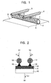
- Fig. 11 is a diagram showing the method for forming a point contact array according to the sixth embodiment of the present invention.
- Ag wires 41 and 42 are formed on an insulating substrate 40.
- the surfaces of the Ag wires are sulfurized to form Ag 2 S films 43 and 44.
- Pt wires 45 and 46 are disposed thereon.
- bridges 47 and 48 comprising Ag atoms are formed at the intersections of the Ag wires 41 and 42 and the Pt wires 45 and 46, the Ag wires 41 and 42 being covered with the Ag 2 S films 43 and 44, respectively.
- the present invention therefore, when the Pt wires 45 and 46 are arranged, a voltage is applied between the Pt wires 45 and 46 and the Ag wires 41 and 42 to precipitate Ag on the Ag 2 S film 43 and 44, resulting in the formation of the bridges 47 and 48. Consequently, when the Pt wires 45 and 46 are arranged using, for example, a wiring system or the like, the present invention can be realized.
- the bridge can be previously formed at each intersection by evaporation of Ag through a mask.
- electron beams can be irradiated on each Ag wire covered with the Ag 2 S film to precipitate Ag atoms. It is important that Ag exists between Ag 2 S functioning as a first electrode and Pt functioning as a second electrode.
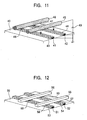
- Fig. 12 is a schematic view of a point contact array according to the seventh embodiment of the present invention, the point contact array controlling the conductivity of each semiconductor.
- Ag wires 51 and 52 are formed on an insulating substrate 50. Further, semiconductors or insulators 57, 58, 59, and 60, which can dissolve Ag atoms, are formed only at the intersections of the Ag wires 51 and 52 and the Pt wires 55 and 56. In Fig. 12, an insulating material covering these components are not shown. All of the components shown in the diagram are embedded in a device.
- Fig. 13 shows an embodiment in which a part of each metallic wire serving as a first electrode is covered with an electronic/ionic mixed conductor. According to the present embodiment, it is enough to form point contacts, each comprising "a metal serving as a first electrode, an electronic/ionic mixed conductor, a bridge or a semiconductor, and a metal serving as a second electrode", at the intersections of the metallic wire functioning as the first electrode and metallic wires each functioning as the second electrode.
- each part which is in contact with the electronic/ionic mixed conductor can be different from a material of the wire between the point contacts.
- Ag wires 79 and 80 are used as parts which are in contact with electronic/ionic mixed conductors (Ag 2 S) 77 and 78, respectively.
- Tungsten wires are used as other parts 81 to 83.
- each part comprise the same element as the mobile ions in the electronic/ionic mixed conductor. According to the present embodiment, therefore, since Ag 2 S is used as the electronic/ionic mixed conductor, Ag is used as a material for the part which is in contact therewith.
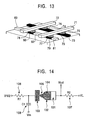
- Fig. 14 is a schematic diagram of a NOT circuit according to a ninth embodiment of the present invention.
- a first electrode 102 serving as an electronic/ionic mixed conductor is formed on a conductive substance 101.
- a potential difference between the first electrode 102 and a second electrode 103 is controlled, thus controlling so that mobile ions (atoms) 104 in the electronic/ionic mixed conductor are precipitated as metallic atoms on the surface of the first electrode 102, alternatively, the precipitated metallic atoms are dissolved as mobile ions (atoms) into the first electrode 102.
- a voltage VH/2 corresponding to a high-level output is applied to the second electrode 103 of the atomic switch through a resistor 106 (resistance R1).
- An input terminal V in is connected to the second electrode 103 through a capacitor 108 (capacitance C1).
- a voltage VL corresponding to a low-level output is applied to the conductive substance 101 functioning as the first electrode 102 of the atomic switch through a resistor 107 (resistance R2).
- An output terminal V out is connected to the conductive substance 101.
- VH is used as a high-level input and VL is used as a low-level input.
- VL is used as a low-level input.
- the output V out indicates VH/2.
- the output V out indicates VL. In other words, when the input is at a high level, the output goes to a low level.
- the input is at a low level, the output goes to a high level.
- the atomic switch functions as a NOT circuit.
- a NOT circuit can be formed using an atomic switch having another electronic/ionic mixed conductor such as Ag 2 Se, Cu 2 S, or Cu 2 Se and a metal other than Pt.
- Switching time ts is almost determined by the capacitance C1 of the capacitor 108 and the resistance R1 of the resistor 106. For instance, when it is assumed that the capacitance C1 of the capacitor is 1 pF and the resistance R1 is 10 ⁇ , switching can be performed on the order of gigahertzs.
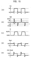
- Fig. 15(e) shows the potential difference between the electrodes 102 and 103 of the atomic switch.
- VL low level
- VH high level
- the NOT circuit according to the present embodiment operates with reliability and stability.
- VH or VL is used as an input and VH/2 or VL is used as an output is described.
- VH - VL a potential difference between inputs
- VH/2 - VL a potential difference between outputs
- the potential difference between inputs and that between outputs can be freely set within the limitations.
- Fig. 16 is a schematic diagram of a NOT circuit according to a tenth embodiment of the present invention.
- a first electrode 112 serving as an electronic/ionic mixed conductor (Ag 2 S) is formed on Ag 111 serving as a conductive substance.
- Mobile ions (Ag ions) 114 in the electronic/ionic mixed conductor are precipitated to form a bridge 115 comprising Ag atoms between the first electrode 112 and a second electrode (Pt) 113.
- An atomic switch with the above structure is used.
- R(ON) denotes a resistance of the atomic switch in the ON state
- R(OFF) denotes a resistance of the atomic switch in the OFF state.
- the resistors and the atomic switch which satisfy the following relation, are used.
- Fig. 17(e) shows the potential difference between the electrodes 112 and 113 of the atomic switch.
- V in is at the low level (VL)
- VH/2 the potential difference between the electrodes 112 and 113 of the atomic switch indicates VH/2. This value indicates a potential difference at which the atomic switch should be in the OFF state. Therefore, the OFF state is held stably.
- the NOT circuit according to the present embodiment operates with reliability and stability.
- Fig. 18 is a schematic diagram of a NOT circuit according to the eleventh embodiment of the present invention.
- Fig. 19 includes graphs showing the principle of operation of the NOT circuit shown in Fig. 18.
- a diode 109 is connected to a portion (V out ' in Fig. 18) corresponding to the output of the NOT circuit according to the ninth embodiment (Fig. 14).
- VH is applied to the other end of the diode 109 through a resistor 110 (resistance R5).
- An output terminal V out is connected to the other end thereof.
- the present NOT circuit differs from the NOT circuit according to the ninth embodiment (Fig. 14) with respect to a point that a voltage to be applied through the resistor 107 (resistance R2) is not VL, but VS.
- V out ' is changed in the same way as the ninth embodiment except that the low level is not VL, but VS [refer to Fig. 19(b)].
- VF denotes a threshold voltage of the diode 109
- the potential difference between inputs is equalized to that between outputs in the NOT circuit.
- V out ' indicates VH/2
- a voltage that is equal to or lower than the threshold voltage is applied to the diode 109.
- RB denotes a resistance of the diode 109 at this time
- RF denotes a resistance thereof when a voltage that is equal to or higher than the threshold.
- the resistor 110 which satisfies the relation of RB » R5 » RF is used.
- Fig. 19(c) shows a voltage to be applied to the diode.
- the resistances and a voltage to be applied are set so as to satisfy the following expressions.
- R 5 / R 2 ( VH - VL ) / ( VL - VF - VS ) VL > VF + VS
- a NOT circuit in which a potential difference between inputs is equivalent to that between outputs can be formed on the basis of the NOT circuit according to the tenth embodiment shown in Fig. 16.
- a diode 119 is connected to a portion (V out ') corresponding to the output of the NOT circuit according to the tenth embodiment (Fig. 16).
- VH is applied to the other end of the diode 119 through a resistor 120 (resistance R6).
- An output terminal V out is connected to the other end thereof.
- the present NOT circuit differs from the NOT circuit according to the tenth embodiment with respect to a point that the voltage applied through the resistor 117 (resistance R4) is not VL, but VS.
- the principle of operation is substantially the same as that of the NOT circuit described in the eleventh embodiment.
- the resistor 120 which satisfies the relation of RB » R6 » RF is used and the resistances and a voltage to be applied are set so as to satisfy the following expressions.
- R 6 / 2 R 4 ( VH - VL ) / ( VL - VF - VS ) VL > VF + VS
- the NOT circuit in which the potential difference between inputs is equivalent to that between outputs can be realized.
- the resistance of the atomic switch is substantially equivalent to R4.
- the diode and the resistor are added to the NOT circuit in which the atomic switch, the resistors, and the capacitor are arranged according to various patterns, the above-mentioned NOT circuit in which the potential difference between inputs is equivalent to that between outputs can be constructed.
- the arrangement of the atomic switch, the resistors, the capacitor, and the diode is not limited to that described in the present embodiment.
- the present invention is characterized in that these devices are used as components.
- Fig. 21 is a schematic diagram of a one-digit binary adder according to a thirteenth embodiment of the present invention.
- the one-digit binary adder comprises a NOT circuit according to the present invention, an AND circuit, and an OR circuit, the AND circuit and the OR circuit each having an atomic switch, will be described.
- the NOT circuit according to the eleventh embodiment shown in Fig. 18 is used.
- the AND circuit and the OR circuit, proposed by the inventors of the present application in Japanese Patent Application No. 2000-334686, are used.
- respective parts corresponding to the NOT circuit, the AND circuit, and the OR circuit are surrounded by dotted lines.
- the present one-digit binary adder comprises two NOT circuits 121 and 122, three AND circuits 123, 124, and 125, and one OR circuit 126.
- the one-digit binary adder which is applied to a computer, can be constructed. This case is one example.
- a NOT circuit, an AND circuit, and an OR circuit can be constructed using two-terminal devices. Accordingly, all of logic circuits can be constructed using only the two-terminal devices.
- a point contact array, a NOT circuit, and an electronic circuit using the same according to the present invention are applicable to a logic circuit, an arithmetic circuit, and a memory device which are nano-scale.
Landscapes
- Engineering & Computer Science (AREA)
- Chemical & Material Sciences (AREA)
- Nanotechnology (AREA)
- Physics & Mathematics (AREA)
- Mathematical Physics (AREA)
- Crystallography & Structural Chemistry (AREA)
- Computer Hardware Design (AREA)
- Theoretical Computer Science (AREA)
- Computing Systems (AREA)
- General Engineering & Computer Science (AREA)
- Manufacturing & Machinery (AREA)
- Semiconductor Memories (AREA)
- Electronic Switches (AREA)
Applications Claiming Priority (3)
| Application Number | Priority Date | Filing Date | Title |
|---|---|---|---|
| JP2000334686A JP4118500B2 (ja) | 2000-11-01 | 2000-11-01 | ポイントコンタクト・アレー |
| JP2001138103A JP4097912B2 (ja) | 2001-05-09 | 2001-05-09 | Not回路及びそれを用いた電子回路 |
| EP01980925A EP1331671B1 (de) | 2000-11-01 | 2001-10-29 | Punktkontaktmatrix und elektronische Schaltung damit |
Related Parent Applications (1)
| Application Number | Title | Priority Date | Filing Date |
|---|---|---|---|
| EP01980925A Division EP1331671B1 (de) | 2000-11-01 | 2001-10-29 | Punktkontaktmatrix und elektronische Schaltung damit |
Publications (3)
| Publication Number | Publication Date |
|---|---|
| EP1662575A2 true EP1662575A2 (de) | 2006-05-31 |
| EP1662575A3 EP1662575A3 (de) | 2006-06-07 |
| EP1662575B1 EP1662575B1 (de) | 2007-10-17 |
Family
ID=26603286
Family Applications (2)
| Application Number | Title | Priority Date | Filing Date |
|---|---|---|---|
| EP01980925A Expired - Lifetime EP1331671B1 (de) | 2000-11-01 | 2001-10-29 | Punktkontaktmatrix und elektronische Schaltung damit |
| EP06001940A Expired - Lifetime EP1662575B1 (de) | 2000-11-01 | 2001-10-29 | Ein NOT-Schaltkreis |
Family Applications Before (1)
| Application Number | Title | Priority Date | Filing Date |
|---|---|---|---|
| EP01980925A Expired - Lifetime EP1331671B1 (de) | 2000-11-01 | 2001-10-29 | Punktkontaktmatrix und elektronische Schaltung damit |
Country Status (6)
| Country | Link |
|---|---|
| US (3) | US7026911B2 (de) |
| EP (2) | EP1331671B1 (de) |
| KR (1) | KR100751736B1 (de) |
| DE (2) | DE60131036T2 (de) |
| TW (1) | TW523983B (de) |
| WO (1) | WO2002037572A1 (de) |
Families Citing this family (39)
| Publication number | Priority date | Publication date | Assignee | Title |
|---|---|---|---|---|
| EP1331671B1 (de) * | 2000-11-01 | 2007-01-24 | Japan Science and Technology Agency | Punktkontaktmatrix und elektronische Schaltung damit |
| CN100448049C (zh) * | 2001-09-25 | 2008-12-31 | 独立行政法人科学技术振兴机构 | 使用固体电解质的电气元件和存储装置及其制造方法 |
| US6815818B2 (en) | 2001-11-19 | 2004-11-09 | Micron Technology, Inc. | Electrode structure for use in an integrated circuit |
| DE10256486A1 (de) * | 2002-12-03 | 2004-07-15 | Infineon Technologies Ag | Verfahren zum Herstellen einer Speicherzelle, Speicherzelle und Speicherzellen-Anordnung |
| WO2005022798A1 (en) | 2003-08-25 | 2005-03-10 | Interdigital Technology Corporation | Enhanced uplink operation in soft handover |
| JP4356542B2 (ja) * | 2003-08-27 | 2009-11-04 | 日本電気株式会社 | 半導体装置 |
| US7046648B2 (en) | 2003-11-05 | 2006-05-16 | Interdigital Technology Corporation | Wireless communication method and apparatus for coordinating Node-B's and supporting enhanced uplink transmissions during handover |
| US7374793B2 (en) | 2003-12-11 | 2008-05-20 | International Business Machines Corporation | Methods and structures for promoting stable synthesis of carbon nanotubes |
| US20050167655A1 (en) | 2004-01-29 | 2005-08-04 | International Business Machines Corporation | Vertical nanotube semiconductor device structures and methods of forming the same |
| US7211844B2 (en) | 2004-01-29 | 2007-05-01 | International Business Machines Corporation | Vertical field effect transistors incorporating semiconducting nanotubes grown in a spacer-defined passage |
| US7829883B2 (en) | 2004-02-12 | 2010-11-09 | International Business Machines Corporation | Vertical carbon nanotube field effect transistors and arrays |
| US20050274609A1 (en) * | 2004-05-18 | 2005-12-15 | Yong Chen | Composition of matter which results in electronic switching through intra- or inter- molecular charge transfer, or charge transfer between molecules and electrodes induced by an electrical field |
| US7109546B2 (en) | 2004-06-29 | 2006-09-19 | International Business Machines Corporation | Horizontal memory gain cells |
| US7960217B2 (en) * | 2004-09-08 | 2011-06-14 | Thomas Schimmel | Gate controlled atomic switch |
| US7741638B2 (en) * | 2005-11-23 | 2010-06-22 | Hewlett-Packard Development Company, L.P. | Control layer for a nanoscale electronic switching device |
| US9965251B2 (en) | 2006-04-03 | 2018-05-08 | Blaise Laurent Mouttet | Crossbar arithmetic and summation processor |
| US7872334B2 (en) * | 2007-05-04 | 2011-01-18 | International Business Machines Corporation | Carbon nanotube diodes and electrostatic discharge circuits and methods |
| WO2009020210A1 (ja) * | 2007-08-08 | 2009-02-12 | National Institute For Materials Science | スイッチング素子とその用途 |
| US20090038832A1 (en) * | 2007-08-10 | 2009-02-12 | Sterling Chaffins | Device and method of forming electrical path with carbon nanotubes |
| US7768812B2 (en) | 2008-01-15 | 2010-08-03 | Micron Technology, Inc. | Memory cells, memory cell programming methods, memory cell reading methods, memory cell operating methods, and memory devices |
| US8034655B2 (en) | 2008-04-08 | 2011-10-11 | Micron Technology, Inc. | Non-volatile resistive oxide memory cells, non-volatile resistive oxide memory arrays, and methods of forming non-volatile resistive oxide memory cells and memory arrays |
| US8211743B2 (en) | 2008-05-02 | 2012-07-03 | Micron Technology, Inc. | Methods of forming non-volatile memory cells having multi-resistive state material between conductive electrodes |
| US8134137B2 (en) | 2008-06-18 | 2012-03-13 | Micron Technology, Inc. | Memory device constructions, memory cell forming methods, and semiconductor construction forming methods |
| US9343665B2 (en) * | 2008-07-02 | 2016-05-17 | Micron Technology, Inc. | Methods of forming a non-volatile resistive oxide memory cell and methods of forming a non-volatile resistive oxide memory array |
| US8411477B2 (en) | 2010-04-22 | 2013-04-02 | Micron Technology, Inc. | Arrays of vertically stacked tiers of non-volatile cross point memory cells, methods of forming arrays of vertically stacked tiers of non-volatile cross point memory cells, and methods of reading a data value stored by an array of vertically stacked tiers of non-volatile cross point memory cells |
| US8427859B2 (en) | 2010-04-22 | 2013-04-23 | Micron Technology, Inc. | Arrays of vertically stacked tiers of non-volatile cross point memory cells, methods of forming arrays of vertically stacked tiers of non-volatile cross point memory cells, and methods of reading a data value stored by an array of vertically stacked tiers of non-volatile cross point memory cells |
| US8289763B2 (en) | 2010-06-07 | 2012-10-16 | Micron Technology, Inc. | Memory arrays |
| US8668361B2 (en) * | 2010-09-22 | 2014-03-11 | Bridgelux, Inc. | LED-based replacement for fluorescent light source |
| US8351242B2 (en) | 2010-09-29 | 2013-01-08 | Micron Technology, Inc. | Electronic devices, memory devices and memory arrays |
| US8759809B2 (en) * | 2010-10-21 | 2014-06-24 | Micron Technology, Inc. | Integrated circuitry comprising nonvolatile memory cells having platelike electrode and ion conductive material layer |
| US8796661B2 (en) | 2010-11-01 | 2014-08-05 | Micron Technology, Inc. | Nonvolatile memory cells and methods of forming nonvolatile memory cell |
| US8526213B2 (en) | 2010-11-01 | 2013-09-03 | Micron Technology, Inc. | Memory cells, methods of programming memory cells, and methods of forming memory cells |
| US9454997B2 (en) | 2010-12-02 | 2016-09-27 | Micron Technology, Inc. | Array of nonvolatile memory cells having at least five memory cells per unit cell, having a plurality of the unit cells which individually comprise three elevational regions of programmable material, and/or having a continuous volume having a combination of a plurality of vertically oriented memory cells and a plurality of horizontally oriented memory cells; array of vertically stacked tiers of nonvolatile memory cells |
| US8431458B2 (en) | 2010-12-27 | 2013-04-30 | Micron Technology, Inc. | Methods of forming a nonvolatile memory cell and methods of forming an array of nonvolatile memory cells |
| US8791447B2 (en) | 2011-01-20 | 2014-07-29 | Micron Technology, Inc. | Arrays of nonvolatile memory cells and methods of forming arrays of nonvolatile memory cells |
| US8488365B2 (en) | 2011-02-24 | 2013-07-16 | Micron Technology, Inc. | Memory cells |
| US8537592B2 (en) | 2011-04-15 | 2013-09-17 | Micron Technology, Inc. | Arrays of nonvolatile memory cells and methods of forming arrays of nonvolatile memory cells |
| US9792985B2 (en) | 2011-07-22 | 2017-10-17 | Virginia Tech Intellectual Properties, Inc. | Resistive volatile/non-volatile floating electrode logic/memory cell |
| WO2016193361A1 (en) | 2015-06-04 | 2016-12-08 | Eth Zurich | Devices, in particular optical or electro-optical devices with quantized operation |
Family Cites Families (26)
| Publication number | Priority date | Publication date | Assignee | Title |
|---|---|---|---|---|
| US3295112A (en) * | 1964-01-10 | 1966-12-27 | Space General Corp | Electrochemical logic elements |
| US4258109A (en) * | 1977-04-25 | 1981-03-24 | Duracell International Inc. | Solid state cells |
| DE2806464C3 (de) * | 1978-02-15 | 1980-09-11 | Garching Instrumente, Gesellschaft Zur Industriellen Nutzung Von Forschungsergebnissen Mbh, 8000 Muenchen | Elektrisches Bauelement |
| US4245637A (en) * | 1978-07-10 | 1981-01-20 | Nichols Robert L | Shutoff valve sleeve |
| DE3004571A1 (de) * | 1980-02-07 | 1981-08-13 | Max-Planck-Gesellschaft zur Förderung der Wissenschaften e.V., 3400 Göttingen | Feste elektrode in einer elektrolytischen zelle |
| FR2521125A1 (fr) * | 1982-02-09 | 1983-08-12 | Centre Nat Rech Scient | Materiaux vitreux a conductivite ionique, leur preparation et leurs applications electrochimiques |
| US4446059A (en) * | 1982-04-15 | 1984-05-01 | E. I. Du Pont De Nemours & Co. | Conductor compositions |
| US4478679A (en) * | 1983-11-30 | 1984-10-23 | Storage Technology Partners | Self-aligning process for placing a barrier metal over the source and drain regions of MOS semiconductors |
| JPS61230426A (ja) | 1985-04-04 | 1986-10-14 | Agency Of Ind Science & Technol | ジヨセフソン直結型否定回路 |
| US5166919A (en) * | 1991-07-11 | 1992-11-24 | International Business Machines Corporation | Atomic scale electronic switch |
| DE69228524T2 (de) * | 1991-12-24 | 1999-10-28 | Hitachi, Ltd. | Atomare Vorrichtungen und atomare logische Schaltungen |
| JP2616875B2 (ja) * | 1993-05-12 | 1997-06-04 | エスエムシー株式会社 | マニホールドバルブ |
| GB2283136A (en) * | 1993-10-23 | 1995-04-26 | Nicotech Ltd | Electric converter circuits |
| US5366936A (en) * | 1993-11-24 | 1994-11-22 | Vlosov Yuri G | Chalcogenide ion selective electrodes |
| EP1046994A3 (de) * | 1994-03-22 | 2000-12-06 | Hyperchip Inc. | Direkte Zellenersetzung für fehlertolerante Architektur mit gänzlich integrierten Systemen und mit Mitteln zur direkten Kommunikation mit Systembediener |
| US5714768A (en) * | 1995-10-24 | 1998-02-03 | Energy Conversion Devices, Inc. | Second-layer phase change memory array on top of a logic device |
| US5761115A (en) * | 1996-05-30 | 1998-06-02 | Axon Technologies Corporation | Programmable metallization cell structure and method of making same |
| JPH09326514A (ja) * | 1996-06-05 | 1997-12-16 | Fujitsu Ltd | 超電導量子干渉素子回路装置 |
| US6087674A (en) * | 1996-10-28 | 2000-07-11 | Energy Conversion Devices, Inc. | Memory element with memory material comprising phase-change material and dielectric material |
| US6825489B2 (en) * | 2001-04-06 | 2004-11-30 | Axon Technologies Corporation | Microelectronic device, structure, and system, including a memory structure having a variable programmable property and method of forming the same |
| AU763809B2 (en) * | 1999-02-11 | 2003-07-31 | Arizona Board Of Regents On Behalf Of The University Of Arizona, The | Programmable microelectronic devices and methods of forming and programming same |
| WO2000070325A1 (fr) * | 1999-05-13 | 2000-11-23 | Japan Science And Technology Corporation | Microscope a balayage a effet tunnel, sa sonde, procede de traitement de la sonde et procede de production d'une structure fine |
| EP1331671B1 (de) * | 2000-11-01 | 2007-01-24 | Japan Science and Technology Agency | Punktkontaktmatrix und elektronische Schaltung damit |
| US7750332B2 (en) * | 2002-04-30 | 2010-07-06 | Japan Science And Technology Agency | Solid electrolyte switching device, FPGA using same, memory device, and method for manufacturing solid electrolyte switching device |
| US6635525B1 (en) * | 2002-06-03 | 2003-10-21 | International Business Machines Corporation | Method of making backside buried strap for SOI DRAM trench capacitor |
| US6952042B2 (en) * | 2002-06-17 | 2005-10-04 | Honeywell International, Inc. | Microelectromechanical device with integrated conductive shield |
-
2001
- 2001-10-29 EP EP01980925A patent/EP1331671B1/de not_active Expired - Lifetime
- 2001-10-29 US US10/363,259 patent/US7026911B2/en not_active Expired - Lifetime
- 2001-10-29 EP EP06001940A patent/EP1662575B1/de not_active Expired - Lifetime
- 2001-10-29 TW TW090126677A patent/TW523983B/zh not_active IP Right Cessation
- 2001-10-29 DE DE60131036T patent/DE60131036T2/de not_active Expired - Lifetime
- 2001-10-29 KR KR1020037004682A patent/KR100751736B1/ko not_active Expired - Fee Related
- 2001-10-29 WO PCT/JP2001/009464 patent/WO2002037572A1/ja not_active Ceased
- 2001-10-29 DE DE60126310T patent/DE60126310T2/de not_active Expired - Lifetime
-
2004
- 2004-08-16 US US10/918,360 patent/US7473982B2/en not_active Expired - Fee Related
-
2005
- 2005-06-24 US US11/165,037 patent/US7525410B2/en not_active Expired - Fee Related
Also Published As
| Publication number | Publication date |
|---|---|
| EP1331671B1 (de) | 2007-01-24 |
| DE60131036T2 (de) | 2008-02-14 |
| EP1662575A3 (de) | 2006-06-07 |
| EP1331671A4 (de) | 2005-05-04 |
| WO2002037572A1 (en) | 2002-05-10 |
| KR20030048421A (ko) | 2003-06-19 |
| US7525410B2 (en) | 2009-04-28 |
| EP1662575B1 (de) | 2007-10-17 |
| US7026911B2 (en) | 2006-04-11 |
| US20030174042A1 (en) | 2003-09-18 |
| DE60126310D1 (de) | 2007-03-15 |
| US20050243844A1 (en) | 2005-11-03 |
| TW523983B (en) | 2003-03-11 |
| DE60131036D1 (de) | 2007-11-29 |
| US7473982B2 (en) | 2009-01-06 |
| EP1331671A1 (de) | 2003-07-30 |
| KR100751736B1 (ko) | 2007-08-27 |
| DE60126310T2 (de) | 2007-06-06 |
| US20050014325A1 (en) | 2005-01-20 |
Similar Documents
| Publication | Publication Date | Title |
|---|---|---|
| EP1331671B1 (de) | Punktkontaktmatrix und elektronische Schaltung damit | |
| JP4979718B2 (ja) | 電気的にプログラム可能な抵抗特性を有するクロスポイントメモリ | |
| CN100448049C (zh) | 使用固体电解质的电气元件和存储装置及其制造方法 | |
| US8767438B2 (en) | Memelectronic device | |
| EP1571673B1 (de) | Speichervorrichtung | |
| US20080237886A1 (en) | Three-dimensional crossbar array systems and methods for writing information to and reading information stored in three-dimensional crossbar array junctions | |
| JPH05505699A (ja) | 強誘電不揮発性可変抵抗素子 | |
| JPWO2003105156A1 (ja) | 不揮発性メモリ回路の駆動方法 | |
| US8716688B2 (en) | Electronic device incorporating memristor made from metallic nanowire | |
| KR20060052550A (ko) | 반도체 메모리 소자 및 반도체 메모리 장치 | |
| JP4118500B2 (ja) | ポイントコンタクト・アレー | |
| JP4119950B2 (ja) | コンダクタンスの制御が可能な電子素子 | |
| CN111406326B (zh) | 磁性存储结构和器件 | |
| US20040151012A1 (en) | Molecular-junction-nanowire-crossbar-based associative array | |
| KR100435924B1 (ko) | 단일전자메모리셀장치 | |
| US8238146B2 (en) | Variable integrated analog resistor | |
| US8331129B2 (en) | Memory array with write feedback | |
| JP4047315B2 (ja) | 記憶素子の値を求めるためのシステム及び方法 | |
| US20200235294A1 (en) | Tunable Resistive Element | |
| Anusudha et al. | Memristor and its applications: a comprehensive review | |
| US20090189642A1 (en) | Nanowire Crossbar Implementations of logic Gates using configurable, tunneling resistor junctions | |
| US20070114679A1 (en) | Multi-terminal hybrid switching device | |
| EP0022266A1 (de) | Halbleiterschaltungsvorrichtung | |
| Kaizawa et al. | Single-electron device with Si nanodot array and multiple input gates | |
| Bengel et al. | Jart vcm v1 verilog-a compact model |
Legal Events
| Date | Code | Title | Description |
|---|---|---|---|
| PUAI | Public reference made under article 153(3) epc to a published international application that has entered the european phase |
Free format text: ORIGINAL CODE: 0009012 |
|
| PUAL | Search report despatched |
Free format text: ORIGINAL CODE: 0009013 |
|
| AC | Divisional application: reference to earlier application |
Ref document number: 1331671 Country of ref document: EP Kind code of ref document: P |
|
| AK | Designated contracting states |
Kind code of ref document: A2 Designated state(s): DE GB NL |
|
| AK | Designated contracting states |
Kind code of ref document: A3 Designated state(s): DE GB NL |
|
| RIN1 | Information on inventor provided before grant (corrected) |
Inventor name: AONA, MASAKAZU Inventor name: NAKAYAMA, TOMONOBU Inventor name: HASEGAWA, TSUYOSHI Inventor name: TERABE, KAZUYA |
|
| 17P | Request for examination filed |
Effective date: 20060809 |
|
| AKX | Designation fees paid |
Designated state(s): DE GB NL |
|
| GRAP | Despatch of communication of intention to grant a patent |
Free format text: ORIGINAL CODE: EPIDOSNIGR1 |
|
| RIC1 | Information provided on ipc code assigned before grant |
Ipc: H01L 45/00 20060101AFI20070328BHEP |
|
| RIN1 | Information on inventor provided before grant (corrected) |
Inventor name: HASEGAWA, TSUYOSHI Inventor name: TERABE, KAZUYA Inventor name: NAKAYAMA, TOMONOBU Inventor name: AONA, MASAKAZU |
|
| GRAS | Grant fee paid |
Free format text: ORIGINAL CODE: EPIDOSNIGR3 |
|
| GRAA | (expected) grant |
Free format text: ORIGINAL CODE: 0009210 |
|
| AC | Divisional application: reference to earlier application |
Ref document number: 1331671 Country of ref document: EP Kind code of ref document: P |
|
| AK | Designated contracting states |
Kind code of ref document: B1 Designated state(s): DE GB NL |
|
| REG | Reference to a national code |
Ref country code: GB Ref legal event code: FG4D |
|
| REF | Corresponds to: |
Ref document number: 60131036 Country of ref document: DE Date of ref document: 20071129 Kind code of ref document: P |
|
| PLBE | No opposition filed within time limit |
Free format text: ORIGINAL CODE: 0009261 |
|
| STAA | Information on the status of an ep patent application or granted ep patent |
Free format text: STATUS: NO OPPOSITION FILED WITHIN TIME LIMIT |
|
| 26N | No opposition filed |
Effective date: 20080718 |
|
| REG | Reference to a national code |
Ref country code: GB Ref legal event code: 732E |
|
| PGFP | Annual fee paid to national office [announced via postgrant information from national office to epo] |
Ref country code: GB Payment date: 20150911 Year of fee payment: 15 |
|
| PGFP | Annual fee paid to national office [announced via postgrant information from national office to epo] |
Ref country code: DE Payment date: 20150911 Year of fee payment: 15 |
|
| PGFP | Annual fee paid to national office [announced via postgrant information from national office to epo] |
Ref country code: NL Payment date: 20150911 Year of fee payment: 15 |
|
| REG | Reference to a national code |
Ref country code: DE Ref legal event code: R119 Ref document number: 60131036 Country of ref document: DE |
|
| REG | Reference to a national code |
Ref country code: NL Ref legal event code: MM Effective date: 20161101 |
|
| GBPC | Gb: european patent ceased through non-payment of renewal fee |
Effective date: 20161029 |
|
| PG25 | Lapsed in a contracting state [announced via postgrant information from national office to epo] |
Ref country code: GB Free format text: LAPSE BECAUSE OF NON-PAYMENT OF DUE FEES Effective date: 20161029 Ref country code: DE Free format text: LAPSE BECAUSE OF NON-PAYMENT OF DUE FEES Effective date: 20170503 |
|
| PG25 | Lapsed in a contracting state [announced via postgrant information from national office to epo] |
Ref country code: NL Free format text: LAPSE BECAUSE OF NON-PAYMENT OF DUE FEES Effective date: 20161101 |