EP1659591A2 - Halbleiterspeicher - Google Patents
Halbleiterspeicher Download PDFInfo
- Publication number
- EP1659591A2 EP1659591A2 EP06002915A EP06002915A EP1659591A2 EP 1659591 A2 EP1659591 A2 EP 1659591A2 EP 06002915 A EP06002915 A EP 06002915A EP 06002915 A EP06002915 A EP 06002915A EP 1659591 A2 EP1659591 A2 EP 1659591A2
- Authority
- EP
- European Patent Office
- Prior art keywords
- transistor
- bit lines
- memory units
- column switch
- data bus
- Prior art date
- Legal status (The legal status is an assumption and is not a legal conclusion. Google has not performed a legal analysis and makes no representation as to the accuracy of the status listed.)
- Granted
Links
Images




Classifications
-
- G—PHYSICS
- G11—INFORMATION STORAGE
- G11C—STATIC STORES
- G11C7/00—Arrangements for writing information into, or reading information out from, a digital store
- G11C7/10—Input/output [I/O] data interface arrangements, e.g. I/O data control circuits, I/O data buffers
- G11C7/1006—Data managing, e.g. manipulating data before writing or reading out, data bus switches or control circuits therefor
-
- G—PHYSICS
- G11—INFORMATION STORAGE
- G11C—STATIC STORES
- G11C11/00—Digital stores characterised by the use of particular electric or magnetic storage elements; Storage elements therefor
- G11C11/21—Digital stores characterised by the use of particular electric or magnetic storage elements; Storage elements therefor using electric elements
- G11C11/34—Digital stores characterised by the use of particular electric or magnetic storage elements; Storage elements therefor using electric elements using semiconductor devices
- G11C11/40—Digital stores characterised by the use of particular electric or magnetic storage elements; Storage elements therefor using electric elements using semiconductor devices using transistors
- G11C11/401—Digital stores characterised by the use of particular electric or magnetic storage elements; Storage elements therefor using electric elements using semiconductor devices using transistors forming cells needing refreshing or charge regeneration, i.e. dynamic cells
- G11C11/4063—Auxiliary circuits, e.g. for addressing, decoding, driving, writing, sensing or timing
- G11C11/407—Auxiliary circuits, e.g. for addressing, decoding, driving, writing, sensing or timing for memory cells of the field-effect type
- G11C11/409—Read-write [R-W] circuits
- G11C11/4096—Input/output [I/O] data management or control circuits, e.g. reading or writing circuits, I/O drivers or bit-line switches
-
- G—PHYSICS
- G11—INFORMATION STORAGE
- G11C—STATIC STORES
- G11C11/00—Digital stores characterised by the use of particular electric or magnetic storage elements; Storage elements therefor
- G11C11/21—Digital stores characterised by the use of particular electric or magnetic storage elements; Storage elements therefor using electric elements
- G11C11/34—Digital stores characterised by the use of particular electric or magnetic storage elements; Storage elements therefor using electric elements using semiconductor devices
- G11C11/40—Digital stores characterised by the use of particular electric or magnetic storage elements; Storage elements therefor using electric elements using semiconductor devices using transistors
- G11C11/401—Digital stores characterised by the use of particular electric or magnetic storage elements; Storage elements therefor using electric elements using semiconductor devices using transistors forming cells needing refreshing or charge regeneration, i.e. dynamic cells
- G11C11/4063—Auxiliary circuits, e.g. for addressing, decoding, driving, writing, sensing or timing
- G11C11/407—Auxiliary circuits, e.g. for addressing, decoding, driving, writing, sensing or timing for memory cells of the field-effect type
- G11C11/409—Read-write [R-W] circuits
- G11C11/4097—Bit-line organisation, e.g. bit-line layout, folded bit lines
-
- G—PHYSICS
- G11—INFORMATION STORAGE
- G11C—STATIC STORES
- G11C29/00—Checking stores for correct operation ; Subsequent repair; Testing stores during standby or offline operation
- G11C29/70—Masking faults in memories by using spares or by reconfiguring
- G11C29/78—Masking faults in memories by using spares or by reconfiguring using programmable devices
- G11C29/84—Masking faults in memories by using spares or by reconfiguring using programmable devices with improved access time or stability
- G11C29/848—Masking faults in memories by using spares or by reconfiguring using programmable devices with improved access time or stability by adjacent switching
-
- H—ELECTRICITY
- H10—SEMICONDUCTOR DEVICES; ELECTRIC SOLID-STATE DEVICES NOT OTHERWISE PROVIDED FOR
- H10B—ELECTRONIC MEMORY DEVICES
- H10B12/00—Dynamic random access memory [DRAM] devices
- H10B12/30—DRAM devices comprising one-transistor - one-capacitor [1T-1C] memory cells
- H10B12/48—Data lines or contacts therefor
- H10B12/482—Bit lines
-
- G—PHYSICS
- G11—INFORMATION STORAGE
- G11C—STATIC STORES
- G11C2207/00—Indexing scheme relating to arrangements for writing information into, or reading information out from, a digital store
- G11C2207/002—Isolation gates, i.e. gates coupling bit lines to the sense amplifier
-
- H—ELECTRICITY
- H10—SEMICONDUCTOR DEVICES; ELECTRIC SOLID-STATE DEVICES NOT OTHERWISE PROVIDED FOR
- H10D—INORGANIC ELECTRIC SEMICONDUCTOR DEVICES
- H10D89/00—Aspects of integrated devices not covered by groups H10D84/00 - H10D88/00
- H10D89/10—Integrated device layouts
Definitions
- sub memory units each have a plurality of bit lines connected to memory cells, respectively, a plurality of sense amplifiers connected to the bit lines, respectively, and a plurality of column switch circuits for connecting the bit lines to data bus lines, respectively.
- the bit lines in each sub memory unit correspond to different data terminals.
- the sub memory units are arranged in a direction orthogonal to a wiring direction of the bit lines.
- This semiconductor memory is formed as a pseudo SRAM which has DRAM memory cells and an SRAM interface.
- the pseudo SRAM has a command decoder 10, an address input circuit 12, a defect information memory part 14, a timing control circuit 16, an address decoder 18, a data input/output circuit 20, and a memory cell array 22.
- the pseudo SRAM also has a refresh timer, a refresh address counter, a refresh control circuit, and the like for performing a refresh operation automatically at predetermined intervals.
- the address input circuit 12 receives an address signal ADD through an address terminal, and outputs the received address signal ADD to the address decoder 18.
- the address signal ADD consists of a plurality of bits of row address signal and a plurality of bits of column address signal.
- the row address signal and the column address signal are supplied to the address terminal at the same timing (address non-multiplexing system).
- the timing control circuit 16 receives a control signal from the command decoder 10, and outputs timing signals for controlling the operation of the memory cell array 22 and the data input/output circuit 20.
- the address decoder 18 decodes the address signal ADD supplied from the address input circuit 12, and outputs the decoding signal ADEC to the memory cell array 22.
- the memory cell array 22 has a column decoder CDEC, a redundancy switch part RSW, a plurality of main memory units MU, and the redundancy memory unit RU.
- the main memory units MU have two sub memory units SU each.
- the redundancy memory unit RU has a single sub memory unit SU. incidentally, the memory cell array 22 has a row decoder, which is omitted from the drawings and description since it is not directly related to the present invention.
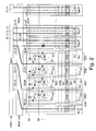
- each of the bit line isolation areas ISO formed for each of the bit line pairs BL, /BL are an nMOS transistor for equalizing the bit lines BL and /BL according to a bit line reset signal BRSL (or BRSR) and nMOS transistors for respectively connecting the bit lines BL, /BL to sense amplifiers formed in the sense amplifier area SA according to a bit line transfer signal BLTR.
- BRSL bit line reset signal
- nMOS transistors for respectively connecting the bit lines BL, /BL to sense amplifiers formed in the sense amplifier area SA according to a bit line transfer signal BLTR.
- the precharge area PRE formed for each of the bit line pairs BL, /BL are nMOS transistors for respectively connecting the bit lines BL, /BL to a precharging power supply line VPR according to a bit line reset signal BRS.
- column switch circuits CSW are formed for the respective bit lines BL and /BL.
- a column switch circuit CSW corresponding to the leftmost bit line BL0 in the diagram has: a first transistor M11 whose drain is connected to a local data bus line LDB0 and whose gate is connected to the second column selecting line CL20 for transmitting the column selecting signal; a second transistor M21 whose gate is connected to the bit line /BL0 and whose source is connected to a ground line (source power supply); a third transistor M31 whose drain is connected to the source of the first transistor M11, whose source is connected to the drain of the second transistor M21, and whose gate receives a read control signal RCL which turns to an activation level in a read operation; and a fourth transistor M41 whose drain is connected to the bit line BL0, whose source is connected to the source of the first transistor M11, and whose gate receives a write control signal WCL which turns to an activation level in a write operation.
- a column switch circuit CSW corresponding to the left bit line /BL0 in the diagram has: a first transistor M12 whose drain is connected to a local data bus line /LDB0 and whose gate is connected to the second column selecting line CL20 for transmitting the column selecting signal; a second transistor M22 whose gate is connected to the bit line BL0 and whose source is connected to the ground line (source power supply); a third transistor M32 whose drain is connected to the source of the first transistor M12, whose source is connected to the drain of the second transistor M22, and whose gate receives the read control signal RCL which turns to the activation level in a read operation: and a fourth transistor M42 whose drain is connected to the bit line /BL0, whose source is connected to the source of the first transistor M12, and whose gate receives the write control signal WCL which turns to the activation level in a write operation,
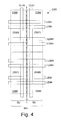
- two local data bus lines LDB are provided for each bit line BL, /BL instead of reducing the number of local data bus lines LDB. Consequently, at the time of defect analysis, the sequence of the bit lines BL, /BL need not be taken into account regardless of whether the product is a relief product or non-relief product. This facilitates the defect analysis. It is therefore possible to reduce the time necessary for the defect analysis.
- the local data bus lines LDB are connected to global data bus lines GDB, respectively, which are laid in the wiring direction of the bit lines BL and /BL.
- the global data bus lines GDB are connected to the common data bus line CD8 shown in Fig. 1 through not-shown read amplifiers and write amplifiers.
- the column switch circuits CSW opposed to each other have different data terminal numbers in the adjoining sub memory units SU.
- the local data bus lines LDB are laid in each row of column switch circuits CSW aligning in the direction orthogonal to the wiring direction of the bit lines BL and /BL. This eliminates the need for the local data bus lines LDB to be curved intricately on the column switch areas CSR, thereby facilitating the wiring layout of the local data bus lines LDB.
Landscapes
- Engineering & Computer Science (AREA)
- Microelectronics & Electronic Packaging (AREA)
- Computer Hardware Design (AREA)
- Databases & Information Systems (AREA)
- For Increasing The Reliability Of Semiconductor Memories (AREA)
- Dram (AREA)
- Semiconductor Memories (AREA)
- Techniques For Improving Reliability Of Storages (AREA)
- Static Random-Access Memory (AREA)
Applications Claiming Priority (2)
| Application Number | Priority Date | Filing Date | Title |
|---|---|---|---|
| JP2002251851A JP4425532B2 (ja) | 2002-08-29 | 2002-08-29 | 半導体メモリ |
| EP03017410A EP1394808B1 (de) | 2002-08-29 | 2003-08-01 | Halbleiterspeicheranordnung |
Related Parent Applications (2)
| Application Number | Title | Priority Date | Filing Date |
|---|---|---|---|
| EP03017410A Division EP1394808B1 (de) | 2002-08-29 | 2003-08-01 | Halbleiterspeicheranordnung |
| EP03017410.6 Division | 2003-08-01 |
Publications (3)
| Publication Number | Publication Date |
|---|---|
| EP1659591A2 true EP1659591A2 (de) | 2006-05-24 |
| EP1659591A3 EP1659591A3 (de) | 2006-06-07 |
| EP1659591B1 EP1659591B1 (de) | 2010-09-22 |
Family
ID=31492619
Family Applications (2)
| Application Number | Title | Priority Date | Filing Date |
|---|---|---|---|
| EP03017410A Expired - Lifetime EP1394808B1 (de) | 2002-08-29 | 2003-08-01 | Halbleiterspeicheranordnung |
| EP06002915A Expired - Lifetime EP1659591B1 (de) | 2002-08-29 | 2003-08-01 | Halbleiterspeicher |
Family Applications Before (1)
| Application Number | Title | Priority Date | Filing Date |
|---|---|---|---|
| EP03017410A Expired - Lifetime EP1394808B1 (de) | 2002-08-29 | 2003-08-01 | Halbleiterspeicheranordnung |
Country Status (4)
| Country | Link |
|---|---|
| US (1) | US6831870B2 (de) |
| EP (2) | EP1394808B1 (de) |
| JP (1) | JP4425532B2 (de) |
| DE (2) | DE60334326D1 (de) |
Families Citing this family (1)
| Publication number | Priority date | Publication date | Assignee | Title |
|---|---|---|---|---|
| KR100845796B1 (ko) | 2006-02-07 | 2008-07-14 | 주식회사 하이닉스반도체 | 반도체 메모리 장치의 데이터 입출력 회로 및 방법 |
Citations (3)
| Publication number | Priority date | Publication date | Assignee | Title |
|---|---|---|---|---|
| US5018101A (en) | 1987-09-16 | 1991-05-21 | Hitachi, Ltd. | Semiconductor memory |
| US5886943A (en) | 1996-09-18 | 1999-03-23 | Hitachi, Ltd. | Semiconductor memory having a hierarchical data line structure |
| JP2002251851A (ja) | 2001-02-26 | 2002-09-06 | Matsushita Electric Ind Co Ltd | ディスク装置 |
Family Cites Families (7)
| Publication number | Priority date | Publication date | Assignee | Title |
|---|---|---|---|---|
| JPH0670880B2 (ja) * | 1983-01-21 | 1994-09-07 | 株式会社日立マイコンシステム | 半導体記憶装置 |
| US5134584A (en) * | 1988-07-22 | 1992-07-28 | Vtc Incorporated | Reconfigurable memory |
| JPH0814985B2 (ja) | 1989-06-06 | 1996-02-14 | 富士通株式会社 | 半導体記憶装置 |
| US5920503A (en) * | 1996-03-29 | 1999-07-06 | Aplus Flash Technology, Inc. | Flash memory with novel bitline decoder and sourceline latch |
| JP2000182390A (ja) | 1998-12-11 | 2000-06-30 | Mitsubishi Electric Corp | 半導体記憶装置 |
| JP2000195291A (ja) * | 1998-12-28 | 2000-07-14 | Oki Electric Ind Co Ltd | 半導体記憶装置及びその冗長救済方法 |
| JP2002008389A (ja) * | 2000-06-20 | 2002-01-11 | Mitsubishi Electric Corp | 半導体記憶装置 |
-
2002
- 2002-08-29 JP JP2002251851A patent/JP4425532B2/ja not_active Expired - Fee Related
-
2003
- 2003-07-29 US US10/628,469 patent/US6831870B2/en not_active Expired - Lifetime
- 2003-08-01 EP EP03017410A patent/EP1394808B1/de not_active Expired - Lifetime
- 2003-08-01 DE DE60334326T patent/DE60334326D1/de not_active Expired - Lifetime
- 2003-08-01 EP EP06002915A patent/EP1659591B1/de not_active Expired - Lifetime
- 2003-08-01 DE DE60332900T patent/DE60332900D1/de not_active Expired - Lifetime
Patent Citations (3)
| Publication number | Priority date | Publication date | Assignee | Title |
|---|---|---|---|---|
| US5018101A (en) | 1987-09-16 | 1991-05-21 | Hitachi, Ltd. | Semiconductor memory |
| US5886943A (en) | 1996-09-18 | 1999-03-23 | Hitachi, Ltd. | Semiconductor memory having a hierarchical data line structure |
| JP2002251851A (ja) | 2001-02-26 | 2002-09-06 | Matsushita Electric Ind Co Ltd | ディスク装置 |
Also Published As
| Publication number | Publication date |
|---|---|
| EP1394808A2 (de) | 2004-03-03 |
| DE60332900D1 (de) | 2010-07-22 |
| JP2004095003A (ja) | 2004-03-25 |
| EP1659591B1 (de) | 2010-09-22 |
| DE60334326D1 (de) | 2010-11-04 |
| EP1659591A3 (de) | 2006-06-07 |
| US6831870B2 (en) | 2004-12-14 |
| EP1394808A3 (de) | 2004-06-23 |
| JP4425532B2 (ja) | 2010-03-03 |
| EP1394808B1 (de) | 2010-06-09 |
| US20040114442A1 (en) | 2004-06-17 |
Similar Documents
| Publication | Publication Date | Title |
|---|---|---|
| US7420860B2 (en) | Semiconductor memory having a dummy signal line connected to dummy memory cell | |
| US4829480A (en) | Column redundancy circuit for CMOS dynamic random access memory | |
| EP1895546B1 (de) | Halbleiterspeicher und -system | |
| JP3631277B2 (ja) | メモリモジュール | |
| JP2004503897A (ja) | 行修理をセグメント化した半導体メモリ | |
| US8339868B2 (en) | Semiconductor device and write control method for semiconductor device | |
| US5430678A (en) | Semiconductor memory having redundant cells | |
| JP2007004953A (ja) | 半導体メモリ | |
| KR100756258B1 (ko) | 반도체 메모리 | |
| US5694368A (en) | Memory device with efficient redundancy using sense amplifiers | |
| US20050068816A1 (en) | Semiconductor memory device and method of testing the device | |
| US6940767B2 (en) | Semiconductor memory device having a plurality of signal lines for writing and reading data | |
| KR100576403B1 (ko) | 메모리 | |
| JP3688443B2 (ja) | 半導体記憶装置 | |
| EP1394808B1 (de) | Halbleiterspeicheranordnung | |
| JP2579792B2 (ja) | 冗長構成半導体メモリ | |
| US6335652B2 (en) | Method and apparatus for the replacement of non-operational metal lines in DRAMS | |
| KR100871964B1 (ko) | 반도체 소자의 테스트 장치 및 방법 | |
| US7154793B2 (en) | Integrated memory and method for functional testing of the integrated memory | |
| JP2004095003A5 (de) | ||
| JPH103799A (ja) | 半導体記憶装置 | |
| JPH04241299A (ja) | 半導体記憶装置の欠陥救済方法及び欠陥救済回路並びにそれを具備する半導体記憶装置 | |
| JP2001297596A (ja) | 半導体集積回路装置 | |
| JPH08293200A (ja) | 半導体記憶装置及び半導体記憶装置の試験装置及び試験方法 |
Legal Events
| Date | Code | Title | Description |
|---|---|---|---|
| PUAI | Public reference made under article 153(3) epc to a published international application that has entered the european phase |
Free format text: ORIGINAL CODE: 0009012 |
|
| PUAL | Search report despatched |
Free format text: ORIGINAL CODE: 0009013 |
|
| AC | Divisional application: reference to earlier application |
Ref document number: 1394808 Country of ref document: EP Kind code of ref document: P |
|
| AK | Designated contracting states |
Kind code of ref document: A2 Designated state(s): DE FR IT |
|
| AK | Designated contracting states |
Kind code of ref document: A3 Designated state(s): DE FR IT |
|
| 17P | Request for examination filed |
Effective date: 20060911 |
|
| 17Q | First examination report despatched |
Effective date: 20061026 |
|
| AKX | Designation fees paid |
Designated state(s): DE FR IT |
|
| RAP1 | Party data changed (applicant data changed or rights of an application transferred) |
Owner name: FUJITSU MICROELECTRONICS LIMITED |
|
| GRAP | Despatch of communication of intention to grant a patent |
Free format text: ORIGINAL CODE: EPIDOSNIGR1 |
|
| RAP1 | Party data changed (applicant data changed or rights of an application transferred) |
Owner name: FUJITSU SEMICONDUCTOR LIMITED |
|
| GRAS | Grant fee paid |
Free format text: ORIGINAL CODE: EPIDOSNIGR3 |
|
| GRAA | (expected) grant |
Free format text: ORIGINAL CODE: 0009210 |
|
| AC | Divisional application: reference to earlier application |
Ref document number: 1394808 Country of ref document: EP Kind code of ref document: P |
|
| AK | Designated contracting states |
Kind code of ref document: B1 Designated state(s): DE FR IT |
|
| REF | Corresponds to: |
Ref document number: 60334326 Country of ref document: DE Date of ref document: 20101104 Kind code of ref document: P |
|
| PG25 | Lapsed in a contracting state [announced via postgrant information from national office to epo] |
Ref country code: IT Free format text: LAPSE BECAUSE OF FAILURE TO SUBMIT A TRANSLATION OF THE DESCRIPTION OR TO PAY THE FEE WITHIN THE PRESCRIBED TIME-LIMIT Effective date: 20100922 |
|
| PLBE | No opposition filed within time limit |
Free format text: ORIGINAL CODE: 0009261 |
|
| STAA | Information on the status of an ep patent application or granted ep patent |
Free format text: STATUS: NO OPPOSITION FILED WITHIN TIME LIMIT |
|
| 26N | No opposition filed |
Effective date: 20110623 |
|
| REG | Reference to a national code |
Ref country code: DE Ref legal event code: R097 Ref document number: 60334326 Country of ref document: DE Effective date: 20110623 |
|
| REG | Reference to a national code |
Ref country code: FR Ref legal event code: ST Effective date: 20120430 |
|
| PG25 | Lapsed in a contracting state [announced via postgrant information from national office to epo] |
Ref country code: FR Free format text: LAPSE BECAUSE OF NON-PAYMENT OF DUE FEES Effective date: 20110831 |
|
| REG | Reference to a national code |
Ref country code: DE Ref legal event code: R082 Ref document number: 60334326 Country of ref document: DE Representative=s name: REICHERT & LINDNER PARTNERSCHAFT PATENTANWAELT, DE |
|
| REG | Reference to a national code |
Ref country code: DE Ref legal event code: R081 Ref document number: 60334326 Country of ref document: DE Owner name: SOCIONEXT INC., YOKOHAMA-SHI, JP Free format text: FORMER OWNER: FUJITSU SEMICONDUCTOR LTD., YOKOHAMA, KANAGAWA, JP Effective date: 20150512 Ref country code: DE Ref legal event code: R082 Ref document number: 60334326 Country of ref document: DE Representative=s name: REICHERT & LINDNER PARTNERSCHAFT PATENTANWAELT, DE Effective date: 20150512 |
|
| PGFP | Annual fee paid to national office [announced via postgrant information from national office to epo] |
Ref country code: DE Payment date: 20160726 Year of fee payment: 14 |
|
| REG | Reference to a national code |
Ref country code: DE Ref legal event code: R119 Ref document number: 60334326 Country of ref document: DE |
|
| PG25 | Lapsed in a contracting state [announced via postgrant information from national office to epo] |
Ref country code: DE Free format text: LAPSE BECAUSE OF NON-PAYMENT OF DUE FEES Effective date: 20180301 |