EP1632996A2 - Integrierte Schaltung mit Kupferleitbahnen und Verfahren zur Herstellung von Kupferleitbahnen - Google Patents
Integrierte Schaltung mit Kupferleitbahnen und Verfahren zur Herstellung von Kupferleitbahnen Download PDFInfo
- Publication number
- EP1632996A2 EP1632996A2 EP05291691A EP05291691A EP1632996A2 EP 1632996 A2 EP1632996 A2 EP 1632996A2 EP 05291691 A EP05291691 A EP 05291691A EP 05291691 A EP05291691 A EP 05291691A EP 1632996 A2 EP1632996 A2 EP 1632996A2
- Authority
- EP
- European Patent Office
- Prior art keywords
- copper
- integrated circuit
- annealing
- copper lines
- temperature
- Prior art date
- Legal status (The legal status is an assumption and is not a legal conclusion. Google has not performed a legal analysis and makes no representation as to the accuracy of the status listed.)
- Withdrawn
Links
Images
Classifications
-
- H—ELECTRICITY
- H10—SEMICONDUCTOR DEVICES; ELECTRIC SOLID-STATE DEVICES NOT OTHERWISE PROVIDED FOR
- H10W—GENERIC PACKAGES, INTERCONNECTIONS, CONNECTORS OR OTHER CONSTRUCTIONAL DETAILS OF DEVICES COVERED BY CLASS H10
- H10W20/00—Interconnections in chips, wafers or substrates
- H10W20/01—Manufacture or treatment
- H10W20/031—Manufacture or treatment of conductive parts of the interconnections
-
- H—ELECTRICITY
- H10—SEMICONDUCTOR DEVICES; ELECTRIC SOLID-STATE DEVICES NOT OTHERWISE PROVIDED FOR
- H10W—GENERIC PACKAGES, INTERCONNECTIONS, CONNECTORS OR OTHER CONSTRUCTIONAL DETAILS OF DEVICES COVERED BY CLASS H10
- H10W20/00—Interconnections in chips, wafers or substrates
- H10W20/01—Manufacture or treatment
- H10W20/031—Manufacture or treatment of conductive parts of the interconnections
- H10W20/056—Manufacture or treatment of conductive parts of the interconnections by filling conductive material into holes, grooves or trenches
-
- H—ELECTRICITY
- H10—SEMICONDUCTOR DEVICES; ELECTRIC SOLID-STATE DEVICES NOT OTHERWISE PROVIDED FOR
- H10W—GENERIC PACKAGES, INTERCONNECTIONS, CONNECTORS OR OTHER CONSTRUCTIONAL DETAILS OF DEVICES COVERED BY CLASS H10
- H10W20/00—Interconnections in chips, wafers or substrates
- H10W20/40—Interconnections external to wafers or substrates, e.g. back-end-of-line [BEOL] metallisations or vias connecting to gate electrodes
- H10W20/41—Interconnections external to wafers or substrates, e.g. back-end-of-line [BEOL] metallisations or vias connecting to gate electrodes characterised by their conductive parts
- H10W20/425—Barrier, adhesion or liner layers
-
- H—ELECTRICITY
- H10—SEMICONDUCTOR DEVICES; ELECTRIC SOLID-STATE DEVICES NOT OTHERWISE PROVIDED FOR
- H10W—GENERIC PACKAGES, INTERCONNECTIONS, CONNECTORS OR OTHER CONSTRUCTIONAL DETAILS OF DEVICES COVERED BY CLASS H10
- H10W20/00—Interconnections in chips, wafers or substrates
- H10W20/40—Interconnections external to wafers or substrates, e.g. back-end-of-line [BEOL] metallisations or vias connecting to gate electrodes
- H10W20/41—Interconnections external to wafers or substrates, e.g. back-end-of-line [BEOL] metallisations or vias connecting to gate electrodes characterised by their conductive parts
- H10W20/44—Conductive materials thereof
- H10W20/4403—Conductive materials thereof based on metals, e.g. alloys, metal silicides
- H10W20/4421—Conductive materials thereof based on metals, e.g. alloys, metal silicides the principal metal being copper
Definitions
- the present invention relates to the formation of copper lines within an integrated circuit.
- hillocks In integrated circuits comprising copper lines, during the deposition of layers of dielectric materials on the copper lines, the formation of copper growths, also called “hillocks", is observed.
- the hillocks result from a structural rearrangement of the thin layers of copper, activated by temperature. They are formed at the grain boundaries of the copper, usually during the deposition of layers of dielectric material on the copper lines, after chemical-mechanical polishing of the copper.
- the density of hillocks depends on the microstructural properties of the copper deposit.
- the influence of the hillocks is harmful because when they grow between the metal lines, they can cause leaks, and even short circuits. Indeed, the size of the hillocks can reach up to 100 nm.
- the Applicant has surprisingly observed that the density and size of the hillocks were greatly reduced when the copper has a ⁇ 001> crystalline orientation of greater than 30% and a ⁇ 111> crystalline orientation of less than 20%.
- this crystalline structure of copper could be obtained by using, during the formation of copper lines, and after the deposition of copper in trenches, a step of annealing the copper in a gas atmosphere of a mixture N 2 / H 2 at more than 6% H 2 , at a temperature between 300 and 450 ° C, for a duration greater than 10 minutes.
- the invention therefore proposes an integrated circuit comprising copper lines, the crystalline structure of copper having a ⁇ 001> crystalline orientation greater than 30% and a ⁇ 111> crystalline orientation of less than 20%.
- the copper lines may comprise metal tracks and interconnecting vias between the metal tracks of different levels.
- the annealing temperature is preferably between 350 and 450 ° C.
- the annealing may be carried out at a pressure of between 8 ⁇ 10 -4 and 1.2 ⁇ 10 5 Pa (ie between 600 and 900 Torr), and preferably at atmospheric pressure.
- the annealing step is preferably carried out at the latest 3 days after the deposition of the copper, preferably at the latest 8 hours after the deposition of the copper, and even more preferably directly after the deposition of the copper.
- the temperature rise phase, up to the annealing temperature, and the temperature descent phase, below the annealing temperature are also under a gaseous atmosphere of a mixture N 2 / H 2 to more than 6% of H 2 .
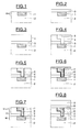
- FIGS. 1 to 8 schematically illustrate the main steps of a mode of implementation of the method of the invention resulting in an embodiment of an integrated circuit according to the invention.
- Figures 1 to 8 are cross-sections of the integrated circuit at different stages of the copper line forming method of the invention.
- Figure 1 shows a line or copper track 1 at the metal level Mn, surrounded by a dielectric material 2.
- the dielectric material 2 is typically FSG (English: Fluorinated Silica Glass).
- a barrier layer 3 of SiN is deposited (FIG. 2) on line 1 in order to prevent copper migration.
- the thickness of the barrier layer 3 is for example of the order of 400 ⁇ .
- the dielectric material 4 is preferably FSG and the thickness of the dielectric material layer 4 is for example of the order of 85 nm.
- the barrier layer 3 and the layer of dielectric material 4 are then etched to form a trench 5.
- the bottom of the trench 5 is constituted by the copper line 1 ( Figure 4).
- the walls of the trench 5 are covered with a barrier layer 6, as shown in Figure 5.
- the material constituting the barrier layer 6 is preferably Ta and / or TaN. It is thus possible to deposit on the walls of the trench a layer of TaN having a thickness of 10 nm, then a layer of Ta having a thickness of 15 nm.
- Copper 7 is then deposited in trench 5, the walls of which are covered with barrier layer 6 (FIG. 6).
- the deposition of the copper 7 can be carried out by any technique known to those skilled in the art, and in particular by electroplating or chemical vapor deposition (CVD).
- Copper annealing 7 takes place under a gaseous atmosphere of a N 2 / H 2 mixture with more than 6% H 2 , at a temperature of between 300 and 450 ° C., for a duration greater than 10 minutes. Below 300 ° C, the annealing is inefficient, and beyond 450 ° C, there is a degradation of the dielectric materials of the integrated circuit.
- the annealing temperature is preferably between 350 and 450 ° C.
- the time between the annealing and the electrolytic deposition step is preferably less than 3 days to avoid degradation of the copper deposit.
- the chemical-mechanical polishing of the copper 7 is then carried out in order to remove the copper 7 which covers the layer of dielectric material 4.
- Figure 7 illustrates the integrated circuit at the end of the chemical mechanical polishing and annealing steps.
- the copper track located at metal level M n + 1 is connected to the metal level track M n via via V n .
- the formation of the integrated circuit is continued by the deposition of a barrier layer 8 of SiN, then of a layer of dielectric material 9, generally by chemical deposition in vapor phase ( Figure 8).
- the thickness of the barrier layer 8 is of the order of 40 nm.
- the dielectric material 9 is preferably FSG and the thickness of the dielectric material layer 9 is of the order of 850 nm.
Landscapes
- Internal Circuitry In Semiconductor Integrated Circuit Devices (AREA)
- Physical Vapour Deposition (AREA)
Applications Claiming Priority (1)
| Application Number | Priority Date | Filing Date | Title |
|---|---|---|---|
| FR0409467A FR2875053A1 (fr) | 2004-09-07 | 2004-09-07 | Circuit integre comprenant des lignes de cuivre et procede de formation de lignes de cuivre |
Publications (1)
| Publication Number | Publication Date |
|---|---|
| EP1632996A2 true EP1632996A2 (de) | 2006-03-08 |
Family
ID=34949144
Family Applications (1)
| Application Number | Title | Priority Date | Filing Date |
|---|---|---|---|
| EP05291691A Withdrawn EP1632996A2 (de) | 2004-09-07 | 2005-08-08 | Integrierte Schaltung mit Kupferleitbahnen und Verfahren zur Herstellung von Kupferleitbahnen |
Country Status (3)
| Country | Link |
|---|---|
| US (1) | US7531447B2 (de) |
| EP (1) | EP1632996A2 (de) |
| FR (1) | FR2875053A1 (de) |
Families Citing this family (4)
| Publication number | Priority date | Publication date | Assignee | Title |
|---|---|---|---|---|
| US9190323B2 (en) | 2012-01-19 | 2015-11-17 | GlobalFoundries, Inc. | Semiconductor devices with copper interconnects and methods for fabricating same |
| WO2017105448A1 (en) * | 2015-12-16 | 2017-06-22 | Intel Corporation | Templated metal apparatus for efficient electric conduction |
| CN111162011B (zh) * | 2020-01-02 | 2022-02-08 | 长江存储科技有限责任公司 | 存储器的制作方法及存储器 |
| US20230069716A1 (en) * | 2021-08-30 | 2023-03-02 | Taiwan Semiconductor Manufacturing Company Limited | Metal interconnect structures and methods of fabricating the same |
Family Cites Families (12)
| Publication number | Priority date | Publication date | Assignee | Title |
|---|---|---|---|---|
| US5391517A (en) * | 1993-09-13 | 1995-02-21 | Motorola Inc. | Process for forming copper interconnect structure |
| US5895274A (en) * | 1996-01-22 | 1999-04-20 | Micron Technology, Inc. | High-pressure anneal process for integrated circuits |
| US5913147A (en) * | 1997-01-21 | 1999-06-15 | Advanced Micro Devices, Inc. | Method for fabricating copper-aluminum metallization |
| US6159857A (en) * | 1999-07-08 | 2000-12-12 | Taiwan Semiconductor Manufacturing Company | Robust post Cu-CMP IMD process |
| US6281110B1 (en) * | 1999-07-27 | 2001-08-28 | Lucent Technologies Inc. | Method for making an integrated circuit including deutrium annealing of metal interconnect layers |
| US6440849B1 (en) * | 1999-10-18 | 2002-08-27 | Agere Systems Guardian Corp. | Microstructure control of copper interconnects |
| KR100407678B1 (ko) * | 2000-06-15 | 2003-12-01 | 주식회사 하이닉스반도체 | 반도체 소자의 구리 금속배선 형성 방법 |
| US6548395B1 (en) * | 2000-11-16 | 2003-04-15 | Advanced Micro Devices, Inc. | Method of promoting void free copper interconnects |
| US6451664B1 (en) * | 2001-01-30 | 2002-09-17 | Infineon Technologies Ag | Method of making a MIM capacitor with self-passivating plates |
| US6562712B2 (en) * | 2001-07-03 | 2003-05-13 | Taiwan Semiconductor Manufacturing Co., Ltd | Multi-step planarizing method for forming a patterned thermally extrudable material layer |
| US6518183B1 (en) * | 2001-09-06 | 2003-02-11 | Taiwan Semiconductor Manufacturing Co., Ltd. | Hillock inhibiting method for forming a passivated copper containing conductor layer |
| KR100979071B1 (ko) * | 2002-02-22 | 2010-08-31 | 에이저 시스템즈 인크 | 이중 배향 다결정성 재료의 화학 기계적 연마 |
-
2004
- 2004-09-07 FR FR0409467A patent/FR2875053A1/fr active Pending
-
2005
- 2005-08-08 EP EP05291691A patent/EP1632996A2/de not_active Withdrawn
- 2005-09-06 US US11/220,353 patent/US7531447B2/en not_active Expired - Fee Related
Also Published As
| Publication number | Publication date |
|---|---|
| US20060060976A1 (en) | 2006-03-23 |
| US7531447B2 (en) | 2009-05-12 |
| FR2875053A1 (fr) | 2006-03-10 |
Similar Documents
| Publication | Publication Date | Title |
|---|---|---|
| US9293473B2 (en) | Method for manufacturing a semiconductor on insulator structure having low electrical losses | |
| EP3420583B1 (de) | Träger für eine halbleiterstruktur | |
| EP1338030B1 (de) | Verfahren zur herstellung eines substrats inbesondere für optik,elektronik oder optoelektronik und danach hergestelltes substrat | |
| FR2817394A1 (fr) | Procede de fabrication d'un substrat notamment pour l'optique, l'electronique ou l'optoelectronique et substrat obtenu par ce procede | |
| FR3104318A1 (fr) | Procédé de formation d'un support de manipulation à haute résistivité pour substrat composite | |
| JPH08232079A (ja) | 新規なタングステン溶着プロセス | |
| WO2006000691A1 (fr) | Support d'epitaxie hybride et son procede de fabrication | |
| EP1290721A1 (de) | Verfahren zur herstellung einer galliumnitrid-schicht | |
| FR3062238A1 (fr) | Support pour une structure semi-conductrice | |
| FR3026558A1 (fr) | Procede d'activation de dopants dans une couche semi-conductrice a base de gan | |
| FR3068506A1 (fr) | Procede pour preparer un support pour une structure semi-conductrice | |
| FR2999801A1 (fr) | Procede de fabrication d'une structure | |
| US7531447B2 (en) | Process for forming integrated circuit comprising copper lines | |
| FR2933235A1 (fr) | Substrat bon marche et procede de fabrication associe | |
| EP1407486B1 (de) | Herstellungsverfahren für einen transistor auf einem soi-substrat | |
| FR3104322A1 (fr) | Procédé de formation d'un substrat de manipulation pour une structure composite ciblant des applications rf | |
| FR3129028A1 (fr) | Procede de preparation d’un substrat support muni d’une couche de piegeage de charges | |
| FR2836159A1 (fr) | Procede de formation de couche de carbure de silicium ou de nitrure d'element iii sur un substrat adapte | |
| FR2976401A1 (fr) | Composant electronique comportant un ensemble de transistors mosfet et procede de fabrication | |
| EP4016585B1 (de) | Elektronische vorrichtung aus siliciumcarbid und ihr herstellungsverfahren | |
| FR3129029A1 (fr) | Procede de preparation d’un substrat support muni d’une couche de piegeage de charges | |
| EP1223614A1 (de) | Verfahren zur Herstellung eines monokristallinen Substrats und integrierter Schaltkreis mit einem solchen Substrat | |
| FR2905799A1 (fr) | Realisation d'un substrat en gan | |
| EP1861873A1 (de) | Verfahren zur herstellung einer heterostruktur mit mindestens einer dicken schicht aus halbleitermaterial | |
| EP1010202B1 (de) | Verfahren zur minimierung des randeffekts durch verdichten der isolationsschicht |
Legal Events
| Date | Code | Title | Description |
|---|---|---|---|
| PUAI | Public reference made under article 153(3) epc to a published international application that has entered the european phase |
Free format text: ORIGINAL CODE: 0009012 |
|
| AK | Designated contracting states |
Kind code of ref document: A2 Designated state(s): AT BE BG CH CY CZ DE DK EE ES FI FR GB GR HU IE IS IT LI LT LU LV MC NL PL PT RO SE SI SK TR |
|
| AX | Request for extension of the european patent |
Extension state: AL BA HR MK YU |
|
| STAA | Information on the status of an ep patent application or granted ep patent |
Free format text: STATUS: THE APPLICATION IS DEEMED TO BE WITHDRAWN |
|
| 18D | Application deemed to be withdrawn |
Effective date: 20100302 |