EP1632876A1 - Übertragungssignalanalyseverfahren, programm und vorrichtung - Google Patents
Übertragungssignalanalyseverfahren, programm und vorrichtung Download PDFInfo
- Publication number
- EP1632876A1 EP1632876A1 EP04745592A EP04745592A EP1632876A1 EP 1632876 A1 EP1632876 A1 EP 1632876A1 EP 04745592 A EP04745592 A EP 04745592A EP 04745592 A EP04745592 A EP 04745592A EP 1632876 A1 EP1632876 A1 EP 1632876A1
- Authority
- EP
- European Patent Office
- Prior art keywords
- output
- analysis
- signal
- waveform
- receiving end
- Prior art date
- Legal status (The legal status is an assumption and is not a legal conclusion. Google has not performed a legal analysis and makes no representation as to the accuracy of the status listed.)
- Withdrawn
Links
Images


Classifications
-
- G—PHYSICS
- G06—COMPUTING OR CALCULATING; COUNTING
- G06F—ELECTRIC DIGITAL DATA PROCESSING
- G06F30/00—Computer-aided design [CAD]
- G06F30/30—Circuit design
- G06F30/36—Circuit design at the analogue level
- G06F30/367—Design verification, e.g. using simulation, simulation program with integrated circuit emphasis [SPICE], direct methods or relaxation methods
Definitions
- the present invention relates generally to a method, program and apparatus for analyzing transmission signals of a circuit board mounted with a CPU whose operating frequency exceeds gigahertz. More particularly the invention relates to a program, method and apparatus for analyzing transmission signals through 3-D electromagnetic field analysis using a random signal of the order of 100 bits.
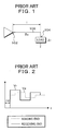
- the reflected wave of the receiving end 104 returns to the sending end 102 and reflects at the sending end again and moves toward the receiving end 104. As long as the reflection coefficient m is not 0 , the reflected wave of the receiving end 104 repeats the above.
- FIG. 2 shows the change caused by reflection of voltage Va of the sending end 102 and voltage Vr of the receiving end 104 shown in FIG. 1. If transmission time is made to be t0 , the signal arrives at the receiving end 104 with the propagation delay time of the line 100. In this situation, the voltage Vr of the receiving end 104 is the sum of the voltage Va of the incident wave from the sending end 102 and the voltage of the reflected wave.
- the reflected wave at this time also arrives at the sending end 102 falling behind just the same td with the propagation time delay of the wiring and reflects.
- the reflected wave is capable of becoming a negative by impedance; therefore, as the reflected wave repeats a reflected wave, the voltage Vr of the receiving end 104 subsides and settles at the voltage Va sent from the sending end 102.
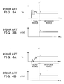
- the load low in the response level is also used for the load Zr at the receiving end 104 when transmission signal frequency is low.
- reflection is repeated before the sensitivity of the load becomes valid at time t1 as shown in FIG. 3A.
- the voltage Vr at the receiving end settles down to a constant voltage or during the rise time of the signal up to time t1 as shown FIG. 4A, the reflection of the voltage Vr settles down and becomes constant. Therefore, the load does not make an error.
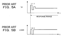
- FIG. 5A illustrates repetition of reflection.
- the load responds to the reflection and acts erratically as shown in FIG. 5B.
- the voltage at the receiving end changes as shown in FIG. 5A in case "111" were sent from the sending end, for example.
- the load makes error of judging the "111” as "101.”
- operating frequency exceeded GHz. To make such a CPU operate normally, it became important to solve the problem of return noise of transmission waveforms.
- a problem of signal transmission in transmission path of a circuit board carrying CPU is that return noise is invariably generated in a transmission waveform. Depending on the row of the signal of 1 and 0, return noise overlaps and sometimes the overlapping reaches the level at which an error occurs.
- the wiring to be analyzed is to be made a model with the electronic circuit components of resistor R, inductance L, and capacitance C.
- resistor R resistor
- L inductance
- C capacitance
- SPICE Simulation Program with Integrated Circuit Emphasis
- FDTD Finite Difference Time-Domain Method
- FDTD Finite Difference Time-Domain Method
- the present invention is intended for a wiring model needing 3-D electromagnetic analysis.
- the object of the invention is to provide a program, method and apparatus for analyzing transmission signals that allow users to obtain the result of analysis of random signals of a multiplicity of bits needed for generating an eye pattern efficiently in short time.
- the present invention provides a transmission signal analysis program.
- the transmission signal analysis program of the invention is operable to cause a computer to execute:
- the analysis step includes analyzing and generating a first output waveform received at the receiving end when a signal pattern changing from 0 to 1 is input to the sending end, and the analysis step includes analyzing and generating a second output waveform received at the receiving end when a signal pattern changing from 1 to 0 is input to the sending end.
- users analyze until the time when return noises on two types of signals changing from 0 to 1 and 1 to 0 settle down. Users then synthesize the signal waveforms of random signals that have a multiplicity of bits needed for displaying eye pattern at a receiving end and the result of analyzing the two types of signals. By employing this method, users can obtain the result of analysis in short time.
- the present invention of this application is based on the following knowledge held by the inventors. It becomes clear that the random signals are two basic types of signal changing from 0 to 1 and 1 to 0 when the input random signals to display eye pattern are decomposed. Therefore, it also becomes clear that the random input signals of these two types of signal can be reproduced at later time by synthesis. The same thing can be said about waveforms at the receiving end after transmission.
- the output signal waveforms of receiving waves obtained by analyzing the basic input signals changing from 0 to 1 and from 1 to 0 are to be said the basic signals decomposed the output signals obtained as the result of transmitting random signals of 100 bits. Accordingly, the results of the transmission of random signals of 100 bits are easily obtained by synthesizing two types of basic output signal waveforms obtained by matching the two types of basic output signal waveforms at the bit position and by analyzing them.
- the analysis step includes analyzing and generating output waveforms for the time a return noise subsides.
- the analysis step includes analyzing and generating output waveforms for the time equal to several times of the signal transmission time.
- the reflection noises of output waveforms at the receiving end reach the level of becoming trouble free as signals repeat going and returning a transmission line 2 or 3 times. Therefore, the analysis of the input signals will be sufficient if it is performed until the signals finish three round trips of the transmission line. The rest will be fine with continuation of the final voltage. No more analysis time is needed.
- the analysis step includes analyzing and generating output waveforms for the time equal to several times of the signal transmission time.
- the analysis step includes using a 3-D electromagnetic analysis of the wiring model to generate the output waveforms .
- the analysis step includes analyzing the output waveforms with the transmission clock frequency of the wiring model equal to or greater than 1 GHz.
- the output waveform generation step includes selecting the first output waveform at bit 1 of the random signal of the predetermined bit count and selecting the second output waveform at bit 0 to generate, for the predetermined bit count, the first output waveform or the second output waveform selected with each bit position as the starting point.
- the waveform synthesis step includes generating a synthesized waveform that reverses for each bit period of the random signal and that has a waveform variation equal to the sum of the positive or negative change of a single or a plurality of output waveforms at each reversal timing.
- the random signal is a bit stream of more than 100 bits.
- the transmission signal analysis program of the present invention is further operable to drive the computer to execute an eye pattern display step, by an eye pattern display unit 26, of generating and displaying an eye pattern from the output waveform generated by the waveform synthesis.
- the present invention provides a transmission signal analysis method.
- the transmission signal analysis method comprises:
- the present invention provides a transmission signal analysis apparatus.
- the transmission signal analysis apparatus comprises:
- the invention is intended for a wiring model and the analysis is performed for the two types of signals changing from 0 to 1 and from 1 to 0.
- the analysis is a 3-D electromagnetic field analysis and is to be done until return noise subsides.
- the output waveforms influenced by return noise at a receiving end are generated.
- the signal waveforms of random signals of a multiplicity of bits at the receiving end needed for displaying eye pattern are generated and synthesized.
- the 3-D electromagnetic analysis in this invention only requires the time needed for the two types of input signals to make round trips of two or three on the transmission line.
- the time needed for processing is only about 30 minutes.
- the result of the analysis can be obtained in about one-tenth of the time in comparison with the time needed for the analysis performed in the past and the method is capable of displaying eye pattern.
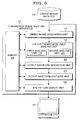
- FIG. 6 is a block diagram of a functional structure showing an embodiment of a transmission signal analysis apparatus according to the invention.
- a transmission signal analysis apparatus 10 is consisted of a wiring model designation unit 14, a 3-D electromagnetic field analysis unit 16, a first analysis unit 18, a second analysis unit 20, an output waveform generation unit 22, an output waveform synthesis unit 24, an eye pattern display unit 26 and a memory 28.
- the wiring model designation unit 14 designates a wiring model from design information on circuit boards such as printed circuit boards stored in a circuit board design data file 12.
- the designated wiring model analyzes transmission signals.
- the wiring model is a model in which a sending end is connected at one end and a receiving end is connected at the other end.
- the sending end is an output for software such as a driver.
- a load is connected at the receiving end.
- FDTD Finite Difference Time-Domain Method
- the first analysis unit 18 placed in the 3-D electromagnetic analysis unit 16 uses the 3-D electromagnetic analysis to analyze a first input signal pattern and to generate a first output waveforms at the receiving end of the wiring model.
- the second analysis unit 20 uses the 3-D electromagnetic analysis to analyze the second input signal pattern and to generate a second output waveforms at the receiving end of the wiring model.
- the output waveform generation unit 22 selects the first waveform generated at the first analysis unit 18 with bit 1 from random signals for creating the eye pattern of 100 bits. Along with the selection, the output waveform generation unit 22 selects the second output waveform generated at the second analysis unit 20 with bit 0 . Then making each bit of the random signals as a starting point generates the first output waveforms or the second output waveforms selected for the number of bits of the random signals.
- the output waveform synthesis unit 24 synthesizes dummy random signals corresponding to the number of bits generated at the output waveform generation unit 22. For example, if the synthesized random signals are 100 bits, the synthesized output waveforms would correspond to 100 bits of dummy random signals. Then when the random signals are input to the sending end of the wiring model, the output waveform synthesis unit 24 generates the output waveforms received at the receiving end. When 100 bits of random signals are obtained at the output waveform synthesis 24, the eye pattern display unit 26 superimposes the output waveforms receiving influences of return noise in the width of 1 bit to create the eye pattern and to display the created eye pattern on a display unit 30.
- the transmission signal analysis apparatus 10 in FIG. 6 is implemented in hardware resources of a computer such as shown in FIG. 7.
- a RAM 102 a hard disk controller (software) 104, a floppy disk driver (software) 110, a CD-ROM driver (software) 114 , a mouse controller 118, a keyboard controller 122, a display controller 126, a communication board 130 are connected to a bus 101 in a CPU 100.
- the hard disk controller 104 is connected to the hard disk drive 106 and loads a program executing transmission signal analysis processing of the invention. When the computer starts, the hard disk controller 104 calls the necessary program from the hard disk drive 106, develops the program on the RAM 102, and executes the program through CPU.
- a floppy disk drive (hardware) 112 is connected to the floppy disk driver 110, reading and writing of a floppy disk (R) is enabled.
- the CD-ROM driver 114 the CD drive (hardware) 116 is connected. The data and programs stored in the CD, therefore, can be read.
- the mouse controller 118 conveys the input operation of a mouse 120 to the CPU 100.
- the keyboard controller 122 conveys the input operation of a keyboard 124 to the CPU 100.
- the display controller 126 executes display on the display unit 128.
- the communication board 130 uses a communication line 132 to communicate through networks such as the Internet.
- the communication board 130 includes wireless networks.
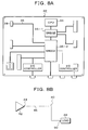
- FIGS. 8A and 8B are explanatory diagrams of a circuit board executing analysis of transmission signals at the signal transmission analysis apparatus 10 in FIG. 6 and a wiring model.
- FIG. 8A is an example of the circuit board 32 to be used for transmission signal analysis.
- This circuit board 32 is equipped with a CPU 34.
- the CPU 34 has a bridge 35-1 and a bridge 35-2. For example, from the bridge 35-2 a bus 36 comes out and the bus is connected to a HDD connector 38 in charge of connecting hard disk drive.
- FIG. 8B takes out the wiring model 40 of the bus 36 in the circuit board 32 in FIG. 8A.
- a driver 42 is placed at one end of a line 46.
- the output end of the driver 42 is a sending end 44.
- a load 48 is connected at the other end of the line 46.
- the connecting point of the load 48 is a receiving end 50.
- the line length of the line 46, the driver 42 of the sending end 44, the load 48 of the receiving end, and the circuit element around the line 46 are all designated by the wiring model designation unit 14 and are input from the circuit design data file 12 to the 3-D electromagnetic analysis unit 16 as designated parameters required for the 3-D electromagnetic field analysis.
- the 3-D electromagnetic field analysis unit 16 sets up the 3-D electromagnetic analysis space in the line 46 of the wiring model 40 when the 3-D electromagnetic field analysis unit receives the input of such designated parameters from the circuit design data file 12 and divides the analysis space into minute rectangular solids (cells) using the rectangular coordinate system. Then the 3-D magnetic field analysis unit 16 uses Maxwell's equation to calculate how electromagnetic waves travel to the receiving end 50 when signals are input to the sending end 44. The targets of calculation include the portion of the line 46 and the electromagnetic field around the line 46. The 3-D magnetic field analysis unit displays the results of the analysis in the representation of voltage (or current) at the end of the analysis.
- FDTD Finite Difference Time-Domain Method
- FIGS. 9A to 9J are time charts decomposing random signals used for the analysis of transmission signal in the invention.
- FIG. 9A is the beginning 8 bits portion of the random input signal Ei. The portion is input to the sending end of the wiring model 40 as shown in FIG. 8B and the waveforms received the influences of the return noise at the receiving end 50 are sought. From these waveforms eye pattern is displayed on the display unit.
- the random input signal Ei to be used for displaying eye pattern usually have the length of about 100 bits. In the invention, the random input signals of 100 bits described above are not used.
- the method employed in the invention is intended for the wiring model shown in FIG 8B and analyzes two types of signals using the 3-D electromagnetic field analysis.
- the two types of signals are the first input signal pattern changing from 0 to 1, the basic signal pattern of the random input signals Ei.
- the second input signal pattern is the signals changing from 1 to 0 in the opposite direction.
- a first output waveform and a second output waveform receiving return noise at the receiving end 50 are generated.
- the output waveforms obtained from the 3-D electromagnetic field analysis of the two types of input signal pattern are synthesized.
- the random input signals Ei originally tried to obtain are input to the sending end 44 of the wiring model 40 to obtain output waveforms receiving influences of return noise at the receiving end 50.
- first bit signal decomposition E1 When a first bit signal decomposition E1 to be 100 bits shown in FIG. 9A is decomposed, it becomes clear that the first bit signal decomposition E1 is the signal synthesized from the signals shown from the first bit decomposition signal E1 to the seventh bit decomposition signal E7 as shown in the signals from FIG. 9B to FIG. H. In this case, the synthesis of the signals from the first bit signal decomposition E1 to the seventh bit signal decomposition E7 is the synthesis as Exclusive Or (EXOR).
- EXOR Exclusive Or
- the decomposition signal of each bit is one of the two types of basic signal in looking at the decomposition signal of each bit decomposed from the random input signal IE.
- the two basic types of signal are the first input signal pattern changing from 0 to 1 shown in FIG. 10A and the second input signal pattern changing from 1 to 0 shown in FIG. 10B.
- the two types of signal shown in FIG. 10A and FIG. 10B are used. At bit 1, the first input signal pattern is selected. Next, at bit 0 the second input signal pattern is selected. At each bit, timing is delayed. In this way, the random input signals Ei as shown in FIG. 9A are synthesized.
- the random input signals Ei is synthesized and reproduced in using the first input signal pattern and the second input signal pattern with timing delay.
- the synthesis and the reproduction are thought to be equal with the case of the input waveforms.
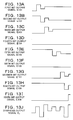
- FIGS. 11A and 11B show the first analysis output pattern in FIG. 11B.
- the first input signal pattern in 11A is input to the sending end 44 of the wiring model 40 in FIG. 8B and the first analysis unit 18 shown in FIG. 6 conducts the 3-D electromagnetic field analysis to obtain the first analysis output pattern at the receiving end 50.
- FIGS. 12A and 12B show the second analysis output pattern in FIG. 12B.
- the second signal pattern in 12A is input to the receiving end 50 of the wiring model 40 in FIG. 8B and the second analysis unit 20 shown in FIG. 6 conducts the 3-D electromagnetic field analysis to obtain the second analysis output pattern at the receiving end 50.
- the analysis output patterns receiving the influences of return noise are obtained through 3-D electromagnetic analysis processing.
- the first analysis output pattern in FIG. 11B and the second analysis output pattern in 12B are synthesized with delay in timing as in the case of the random input signal Ei in FIGS. 9A to 9J. From this synthesis, the random input signals Ei of 100 bits are transmitted and the output waveforms receiving return noise obtained at receiving end 50 are generated. The output waveforms are needed for displaying eye pattern.
- FIGS. 13A to 13J are time charts of the output signals at the receiving end 50 of the wiring model shown in FIG. 8B generated matching each bit of the random input signal Ei shown in FIG. 9A in timing and the synthesis output signal.
- the first bit of the random input signal Ei shown in FIG. 9A is bit 1. Therefore, the first bit output signal E101 of FIG. 13A selects the first analysis output pattern shown in FIG. 11B.
- the second bit of the random input signal Ei shown in FIG. 9A is 0. Therefore, for the second bit output signal E102 in FIGS. 13A to 13J the second analysis output pattern in FIG. 12B is selected and generation is done delaying timing for 1 bit to the first output signal E101.
- the third bit, the fourth bit, the fifth bit, the sixth bit, and the seventh bit are also handled in the same way.
- the first analysis output pattern in FIG. 11B or the second analysis output pattern in FIG. 12B is selected for generation corresponding to the bit "110010" in the random input signal Ei delaying timing by each bit as shown in the output signal from FIG. 13C to FIG. 13G.
- FIGS. 13A to 13J show as far as the seventh bit. Illustration on bits to be followed the seventh bit is omitted.
- FIGS. 13A to 13J show the synthesis of the portion from the output signals E101 to E107 of the first bit to the seventh bit.
- the synthesis of the output signal of each bit is determined by bit period of the random input signal Ei.
- waveform synthesis is conducted as the total of the positive or negative change of 1 or plural output waveforms in each timeliness for judgment to be the waveform change of the synthesis output signal.
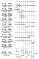
- FIGS. 14A to 14J specifically show the generation of the synthesis output signals in synthesis of the first bit output signal E101 to the seventh signal E107.
- change of the rising portion of the output signal is to be plus and the change in the falling portion is to be minus.
- the change of each bit is shown in the amount of change a to r.
- time t1 the variation of the first bit output signal E101 + a becomes synthesis output signal EO.
- time t2 the sum of the variation of the falling portion of the first bit output signal E101 and the variation of the second bit output signal E102 (b + c) becomes the variation of the synthesis output signal EO.
- the variation of the output signal of the synthesis becomes (g + h).
- the variation of the third bit output signal E103 is +i.
- the variation of the fourth bit output signal E104 is -j, and the variation of the synthesis output signal EO is (j - i) in this case because the variation is to the opposite direction.
- the variation of the synthesis output signal EO is the additional value corresponding to the direction of plus minus of the variation of the bit output signal changing each time.
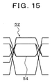
- FIG. 15 shows an eye pattern obtained from the generated synthesis output signal EO as in FIG. 13H.
- this eye pattern 52 every 1 bit of the synthesis output signal EO of FIG. 13H is superimposed on top of another and displayed as widely known.
- an arrow 54 clearly indicates the portion indicated by the arrow 54 is the bad portion reaching the level the load error occurs due to the return noise.
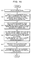
- FIG.16 is a flowchart of a transmission signal analysis processing according to the present invention.
- the processing steps in the flowchart represent the processing steps of the transmission signal analysis processing program according to the present invention. The following is an explanation of the transmission signal analysis processing with FIG. 2
- the processing time of the transmission signal analysis processing is mainly time needed for generation processing for the output waveforms at the receiving end through the 3-D electromagnetic analysis intended for the wiring model of the two types of the first input signal pattern and the second input signal pattern in Steps S2 and S3.
- the generation of the output waveforms at the receiving end through the 3-D electromagnetic field analysis was performed with the entire bits of dummy random signal with 100 bits.
- the method of this invention is limited to the two types of input signal patterns.
- the processing time of this invention saves time substantially.
- the processing time is one tenth of the time needed in the past. Specifically, if five hours are needed for the 3-D electromagnetic field analysis with the use of the random signals of 100 bits, for example, the analysis according to the invention can come up with the result in about 30 minutes. It is because in the invention the analysis of the two types of the input signal pattern is performed until the round trip of the transmission line for three times are executed. It is because after the round trip of two or three times, the influences of the return noise fall to the level that is simply ignored. After that what is needed is to keep the last voltage.
- the processing speed can be raised nearly ten times of that of the conventional transmission line analysis assuming the conventional analysis is the transmission line analysis that uses the 3-D electromagnetic field analysis to display eye pattern.
- the processing time increases as the number of bits of the random signals increases in the analysis processing using the conventional 3-D electromagnetic field analysis to display eye pattern. Even if the number of bits of the random signals increases, the processing to perform the 3-D electromagnetic field analysis is the same as the processing of the two or three times on two types of input signal patterns in this invention. Therefore, the processing time scarcely increases even if the number of bits of the random signals doubles to 200.
- the transmission signal analysis apparatus of the invention is intended for transmission signal analysis in the circuit board that needs the 3-D electromagnetic field analysis whose operating frequency of CPU exceeds 1GHz.
- the invention can be applied equally to the operating frequency having problems with return noise even if the operating frequency is less than 1 GHz.
- FDTD Finite Difference Time-Domain Method
- FEM Finite Element Method
- BEM Boundary Element Method
Landscapes
- Engineering & Computer Science (AREA)
- Computer Hardware Design (AREA)
- Physics & Mathematics (AREA)
- Theoretical Computer Science (AREA)
- Microelectronics & Electronic Packaging (AREA)
- Evolutionary Computation (AREA)
- Geometry (AREA)
- General Engineering & Computer Science (AREA)
- General Physics & Mathematics (AREA)
- Tests Of Electronic Circuits (AREA)
- Monitoring And Testing Of Transmission In General (AREA)
- Design And Manufacture Of Integrated Circuits (AREA)
Applications Claiming Priority (2)
| Application Number | Priority Date | Filing Date | Title |
|---|---|---|---|
| PCT/JP2003/007329 WO2004111886A1 (ja) | 2003-06-10 | 2003-06-10 | 伝送信号解析方法、プログラム及び装置 |
| PCT/JP2004/007816 WO2004111889A1 (ja) | 2003-06-10 | 2004-06-04 | 伝送信号解析プログラム、方法及び装置 |
Publications (2)
| Publication Number | Publication Date |
|---|---|
| EP1632876A1 true EP1632876A1 (de) | 2006-03-08 |
| EP1632876A4 EP1632876A4 (de) | 2007-01-10 |
Family
ID=33548972
Family Applications (1)
| Application Number | Title | Priority Date | Filing Date |
|---|---|---|---|
| EP04745592A Withdrawn EP1632876A4 (de) | 2003-06-10 | 2004-06-04 | Übertragungssignalanalyseverfahren, programm und vorrichtung |
Country Status (4)
| Country | Link |
|---|---|
| US (1) | US7398504B2 (de) |
| EP (1) | EP1632876A4 (de) |
| JP (1) | JP4185098B2 (de) |
| WO (2) | WO2004111886A1 (de) |
Families Citing this family (4)
| Publication number | Priority date | Publication date | Assignee | Title |
|---|---|---|---|---|
| JP2009238130A (ja) * | 2008-03-28 | 2009-10-15 | Fujitsu Ltd | プリント基板設計装置およびプリント基板設計方法 |
| JP5716604B2 (ja) * | 2011-08-08 | 2015-05-13 | 富士通株式会社 | 回路シミュレータプログラム,装置およびアイパターン生成方法 |
| US9768833B2 (en) * | 2014-09-15 | 2017-09-19 | At&T Intellectual Property I, L.P. | Method and apparatus for sensing a condition in a transmission medium of electromagnetic waves |
| JP6865112B2 (ja) * | 2017-06-06 | 2021-04-28 | 矢崎総業株式会社 | 信号処理装置 |
Family Cites Families (5)
| Publication number | Priority date | Publication date | Assignee | Title |
|---|---|---|---|---|
| JP3655106B2 (ja) * | 1998-05-14 | 2005-06-02 | 富士通株式会社 | ノイズチェック装置 |
| JP3639116B2 (ja) * | 1998-06-12 | 2005-04-20 | 富士通株式会社 | 電磁波解析装置及び電磁波解析プログラムを記録したコンピュータ読み取り可能な記録媒体 |
| JP2002032424A (ja) * | 2000-07-13 | 2002-01-31 | Mitsubishi Electric Corp | 回路解析装置、回路解析方法およびその方法をコンピュータに実行させるプログラムを記録したコンピュータ読み取り可能な記録媒体 |
| JP3892256B2 (ja) * | 2000-09-08 | 2007-03-14 | 富士通株式会社 | 信号波形シミュレーション装置、信号波形シミュレーション方法および信号波形シミュレーションプログラムを記録したコンピュータ読み取り可能な記録媒体 |
| US7149666B2 (en) * | 2001-05-30 | 2006-12-12 | University Of Washington | Methods for modeling interactions between massively coupled multiple vias in multilayered electronic packaging structures |
-
2003
- 2003-06-10 WO PCT/JP2003/007329 patent/WO2004111886A1/ja not_active Ceased
-
2004
- 2004-06-04 EP EP04745592A patent/EP1632876A4/de not_active Withdrawn
- 2004-06-04 JP JP2005506895A patent/JP4185098B2/ja not_active Expired - Fee Related
- 2004-06-04 WO PCT/JP2004/007816 patent/WO2004111889A1/ja not_active Ceased
-
2005
- 2005-08-15 US US11/203,118 patent/US7398504B2/en not_active Expired - Fee Related
Also Published As
| Publication number | Publication date |
|---|---|
| WO2004111889A1 (ja) | 2004-12-23 |
| US20050273740A1 (en) | 2005-12-08 |
| EP1632876A4 (de) | 2007-01-10 |
| JP4185098B2 (ja) | 2008-11-19 |
| US7398504B2 (en) | 2008-07-08 |
| JPWO2004111889A1 (ja) | 2006-07-20 |
| WO2004111886A1 (ja) | 2004-12-23 |
Similar Documents
| Publication | Publication Date | Title |
|---|---|---|
| US7469391B2 (en) | Method and device of analyzing crosstalk effects in an electronic device | |
| US8938376B2 (en) | Simulating the transmission and simultaneous switching output noise of signals in a computer system | |
| US6915249B1 (en) | Noise checking method and apparatus | |
| JP2009238130A (ja) | プリント基板設計装置およびプリント基板設計方法 | |
| JP3153403B2 (ja) | 半導体集積回路の遅延時間計算装置 | |
| US6925430B2 (en) | Method of and apparatus for signal-waveform simulation, and computer product | |
| EP3080918A1 (de) | Gegensprechanalyseverfahren mit einer übergeordneten position | |
| US20050268264A1 (en) | Apparatus and method for calculating crosstalk | |
| US20160253448A1 (en) | Circuit board design system, circuit board design method and program recording medium | |
| JP2002164434A (ja) | 不要輻射解析方法および不要輻射解析装置 | |
| US7398504B2 (en) | Program, method and apparatus for analyzing transmission signals | |
| WO1999059089A1 (en) | Noise checking method and device | |
| US7788076B2 (en) | Interference analysis method, interference analysis device, interference analysis program and recording medium with interference analysis program recorded thereon | |
| US6505338B1 (en) | Computer readable medium with definition of interface recorded thereon, verification method for feasibility to connect given circuit and method of generating signal pattern | |
| US6871329B2 (en) | Design system of integrated circuit and its design method and program | |
| KR100999016B1 (ko) | 반도체 장치에 대한 동시 동작 신호 노이즈에 기초하여 지터를 견적하는 방법, 그 견적에 사용하는 동시 동작 신호노이즈량 대 지터량 상관 관계를 산출하는 방법, 이들을 실현하는 프로그램을 기록한 기록매체, 및 반도체 장치 및 그것이 탑재된 프린트 회로 기판의 설계 방법 | |
| US6959250B1 (en) | Method of analyzing electromagnetic interference | |
| JP5040463B2 (ja) | クロストークノイズ解析方法 | |
| US7308620B1 (en) | Method to obtain the worst case transmit data and jitter pattern that minimizes the receiver's data eye for arbitrary channel model | |
| Yasunaga et al. | The design of segmental-transmission-line for high-speed digital signals using genetic algorithms | |
| JP2005100171A (ja) | 対策済回路図作成装置、電子回路基板設計装置、対策済回路図作成方法、対策済回路図作成プログラム、および該プログラムを記録した記録媒体 | |
| US20090299719A1 (en) | Circuit simulation apparatus and method,medium containing circuit simulation program | |
| JP7151403B2 (ja) | 解析装置、解析方法、および解析プログラム | |
| US20060071821A1 (en) | Method for verifying a circuit function | |
| JP2576355B2 (ja) | 遅延最適化方法 |
Legal Events
| Date | Code | Title | Description |
|---|---|---|---|
| PUAI | Public reference made under article 153(3) epc to a published international application that has entered the european phase |
Free format text: ORIGINAL CODE: 0009012 |
|
| 17P | Request for examination filed |
Effective date: 20050830 |
|
| AK | Designated contracting states |
Kind code of ref document: A1 Designated state(s): DE FR GB |
|
| DAX | Request for extension of the european patent (deleted) | ||
| RBV | Designated contracting states (corrected) |
Designated state(s): DE FR GB |
|
| A4 | Supplementary search report drawn up and despatched |
Effective date: 20061207 |
|
| 17Q | First examination report despatched |
Effective date: 20100602 |
|
| STAA | Information on the status of an ep patent application or granted ep patent |
Free format text: STATUS: THE APPLICATION IS DEEMED TO BE WITHDRAWN |
|
| 18D | Application deemed to be withdrawn |
Effective date: 20160105 |