EP1631980B1 - Verfahren zum integrieren von germanium in cmos-prozessen - Google Patents
Verfahren zum integrieren von germanium in cmos-prozessen Download PDFInfo
- Publication number
- EP1631980B1 EP1631980B1 EP04718583.0A EP04718583A EP1631980B1 EP 1631980 B1 EP1631980 B1 EP 1631980B1 EP 04718583 A EP04718583 A EP 04718583A EP 1631980 B1 EP1631980 B1 EP 1631980B1
- Authority
- EP
- European Patent Office
- Prior art keywords
- layer
- silicon oxynitride
- germanium
- depositing
- silicon
- Prior art date
- Legal status (The legal status is an assumption and is not a legal conclusion. Google has not performed a legal analysis and makes no representation as to the accuracy of the status listed.)
- Expired - Lifetime
Links
Images

Classifications
-
- H—ELECTRICITY
- H10—SEMICONDUCTOR DEVICES; ELECTRIC SOLID-STATE DEVICES NOT OTHERWISE PROVIDED FOR
- H10D—INORGANIC ELECTRIC SEMICONDUCTOR DEVICES
- H10D84/00—Integrated devices formed in or on semiconductor substrates that comprise only semiconducting layers, e.g. on Si wafers or on GaAs-on-Si wafers
- H10D84/01—Manufacture or treatment
- H10D84/0123—Integrating together multiple components covered by H10D12/00 or H10D30/00, e.g. integrating multiple IGBTs
- H10D84/0126—Integrating together multiple components covered by H10D12/00 or H10D30/00, e.g. integrating multiple IGBTs the components including insulated gates, e.g. IGFETs
- H10D84/0165—Integrating together multiple components covered by H10D12/00 or H10D30/00, e.g. integrating multiple IGBTs the components including insulated gates, e.g. IGFETs the components including complementary IGFETs, e.g. CMOS devices
- H10D84/0188—Manufacturing their isolation regions
-
- H—ELECTRICITY
- H10—SEMICONDUCTOR DEVICES; ELECTRIC SOLID-STATE DEVICES NOT OTHERWISE PROVIDED FOR
- H10D—INORGANIC ELECTRIC SEMICONDUCTOR DEVICES
- H10D84/00—Integrated devices formed in or on semiconductor substrates that comprise only semiconducting layers, e.g. on Si wafers or on GaAs-on-Si wafers
- H10D84/01—Manufacture or treatment
- H10D84/02—Manufacture or treatment characterised by using material-based technologies
- H10D84/03—Manufacture or treatment characterised by using material-based technologies using Group IV technology, e.g. silicon technology or silicon-carbide [SiC] technology
- H10D84/038—Manufacture or treatment characterised by using material-based technologies using Group IV technology, e.g. silicon technology or silicon-carbide [SiC] technology using silicon technology, e.g. SiGe
-
- Y—GENERAL TAGGING OF NEW TECHNOLOGICAL DEVELOPMENTS; GENERAL TAGGING OF CROSS-SECTIONAL TECHNOLOGIES SPANNING OVER SEVERAL SECTIONS OF THE IPC; TECHNICAL SUBJECTS COVERED BY FORMER USPC CROSS-REFERENCE ART COLLECTIONS [XRACs] AND DIGESTS
- Y10—TECHNICAL SUBJECTS COVERED BY FORMER USPC
- Y10S—TECHNICAL SUBJECTS COVERED BY FORMER USPC CROSS-REFERENCE ART COLLECTIONS [XRACs] AND DIGESTS
- Y10S438/00—Semiconductor device manufacturing: process
- Y10S438/958—Passivation layer
Definitions
- the invention relates generally to the field of chip manufacturing process, and more particularly to fabrication with one or more germanium layers.
- EP 0 484 056 A1 discloses a process for forming a germanium-containing layer on an oxygen-containing insulation layer.
- WO 02/33755 A2 discloses a process for integration of an epitaxial SiGeC photodiode with CMOS structures.
- a silicon nitride (Si 3 N 4 ) film is deposited on a silicon wafer substrate and etched back to result in silicon nitride spacers.
- a step of selective epitaxial growth of a photodiode module on selected active areas is performed, comprising epitaxial growth of a stack of thin silicon alloy films with a specific range of germanium and/or carbon atomic concentration.
- WO 01/01465 A1 discloses a configuration in which a lateral germanium photodetector is integrated with silicon CMOS devices.
- features of some embodiments include the deposition of one or more Germanium (Ge) layers during a standard CMOS process on a monolithic device.
- Ge Germanium
- the insertion of one or more Ge layers enables light to be easily converted into electrical signals.
- Standard metals can be attached directly to the Ge in completing an electrical circuit. Vias can also be used to connect to a Ge layer.
- CMOS complementary metal-oxide-semiconductor
- a silicon oxynitride (SON) layer is used as a mask for selective Ge growth on the Si area left uncovered by the SON patterning.
- a thin Ge layer is then deposited from a germane Chemical-Vapor Deposition (CVD) carried out at a temperature below, for example, a temperature of 370 °C can be used if the reacting gas contains germane. Below this temperature, the Hydrogen (H) contained in the process gas may saturate the dangling bonds of the growing surface, thereby modifying the surface energy.
- CVD Chemical-Vapor Deposition
- the surfactant action of the Hydrogen hinders the islanding phenomenon (Stranski-Krastanov growth) in the Germanium/Silicon (Ge/Si) heterostructure. It also relaxes the strain forcing the misfit dislocation insertion at the heterojunction, thus providing a seed for the nucleation of a strain-relaxed Ge film.
- the growth of this layer wick occurs only on the opening in the SON mask because the germane-deposition catalysis on the SON surface is not effective.
- a thicker Ge layer is deposited at a higher deposition temperature (for example, greater than 600° C) in order to have, for example a layer-by-layer growth mode. The higher temperature also allows an increase in the growth rate.
- a post-growth annealing process may be performed.
- the film undergoes a thermal cycling treatment typically between about 700 °C and 900 °C.
- the film thus obtained is mono-crystalline, epitaxial, and has a small surface roughness (about 1 nm RMS roughness expected).
- CMOS complementary metal-oxide-semiconductor
- a low temperature (for example, T ⁇ 500° C) poly-Ge film is deposited on a Si active area.
- This deposition is catalyzed by a seed layer made of either poly/amorphous-Si or amorphous-Ge. Due to the electronic surface states on the crystallite boundaries, the film is "unintentionally p-doped" typically in the 10 18 cm -3 range: the Fermi level is in fact pinned close to the top of the Ge valence band.
- some embodiments provide the capability of converting an optical signal carried at a wavelength range that can be absorbed by the germanium into an electrical signal.
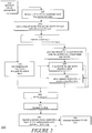
- step 110 the manufacturing of a chip employs a standard CMOS flow with a silicon substrate.
- the process 100 continues until the highest temperature step, typically the salicide annealing, is performed.
- step 120 the process 100 deposits a first silicon oxynitride layer.
- Step 120 is typically a conventional CMOS process step.
- One of ordinary skill in the art should recognize that the deposition of one or more silicon oxynitride layers is typical in a CMOS process. Similar or various types of compositions of silicon oxynitride can be practiced.
- the first oxynitride layer is then patterned in order to expose areas of the underlying Si substrate in the process step 130.
- the scope of the present invention extends to choosing the dielectric film with properties such that the germanium will not grow on the film.
- variations in the present material systems, as well as new material systems that carry the properties as described above, such as low-k dielectrics, can be practiced, while the invention is defined in appended claim 1.
- the present invention concerns germanium growth in a standard CMOS process.
- germanium growth can also be incorporated in BICMOS, SOI, SiGe BICMOS, SOS, and other similar manufacturing processes.
- a window is opened in the first silicon oxynitride layer exposing the active silicon (Si) layer.
- the shape of the opening depends on photonic and material factors.
- the active windows crated in step 130 have rectangular shapes with sides oriented along the ⁇ 011> silicon crystallographic direction. Windows oriented in other crystalline directions could also be fabricated.
- the feedback on the optimal shape of the active Si layer is provided by the morphological and structural characteristics of the Ge deposited on the active Si layer.
- the process 100 performs an epi-clean step 140 on the silicon oxynitride patterned substrate formed in step 130. After a layer removal of the silicon oxynitride layer, an epi-like active silicon surface is recovered. In this procedure, an ex-situ wet chemical cleaning based on hydrofluoric acid (HF) solution is followed by an in-situ annealing in dihydrogen/DCS atmosphere.
- the substrate temperature is approximately 700° C.
- Windows in to the SON layer formed during step 120 and 130 are designed as test structures in order to perform a direct morphological inspection by means of Scanning Probe Microscopy on test wafers which have been pulled out from the process after the step 140.
- Pyramidal-shaped defects are expected to be formed by Si-O and Si-C surface contamination.
- Substrate cleanliness can be evaluated also by growing a Si buffer layer by silane CVD and evaluating the pit defect density and morphology. These defects are formed at the substrate-epilayer interface, and provides a marker of the substrate surface quality.
- the compatibility of the high temperature step relative to the entire fabrication process should be verified.
- the implanted doping distribution and the effect of the thermal stress on the existing structures are monitored.
- a thin Ge layer is deposited at a low temperature for strain relaxation in the lattice mismatched Ge/Si heterostructure.
- a temperature as low as 370° C and a deposition rate of the order of 3-5 nm/min are typical values for this growth step using germane on clean silicon.
- Growth dynamics is characterized and optimized in this step.
- An objective is to optimize the kinetics/thermodynamics of the germane chemisorption at the Si surface.
- the parameters that may vary include: total reaction-gas pressure, partial pressure of the Ge in the H carrier gas, substrate temperature, and amount of deposited material.
- the optimization feedback is provided by investigating the structural, morphological, and electrical properties of the deposited material. Other factors are also evaluated in this step including the growth rate, the incubation time, the defect density, and the stress relaxation via misfit dislocation insertion and/or surface roughening. These quantities are correlated with the shape and size of the opening in the first silicon oxynitride layer formed in step 130 where the material has to be deposited in step 150 and 160.
- One objective in step 150 is to find the optimal thickness for the stress relaxation with the lowest density of point defects with a smooth surface.
- a Ge layer thickness in the 30 to 70 nm range is typical AFM/SEM measurement, a ⁇ -Raman measurement, and an XTEM measurement are performed in order to investigate the morphological and structural properties of the Ge deposited film. Measurements are conducted on window openings of the silicon oxynitride windows formed in step 130 which have a size and shape suitable for an optoelectronics application. In larger windows which can be used for metrology purposes, the growth selectivity is also investigated using a process such as spatially resolved SIMS -Secondary Ion Mass Spectroscopy. Devices are designed to test the compatibility of this process step with the entire production flow.
- step 160 there is a high temperature deposition of a Ge (HTGE - high temperature Ge) active layer, which serves as the core of an active region.
- a Ge HTGE - high temperature Ge
- the Ge growth proceeds in a quasi-homoepitaxial manner.
- the high temperature of the deposition promotes the growth in a layer-by-layer mode, leading to both a desirable crystal quality and a smooth film surface.
- the higher temperature also changes the surface reaction, allowing an increased growth rate.
- Typical values for this step are deposition temperatures between 600-700° C and a growth rate of 10-20 nm/min.
- the deposited film thickness is dependent on the device design: 300 nm can be a guidelines.
- This design takes into account the upper limit of Ge thickness due to the layer thickness of the dielectric stack subsequently deposited, and the length of the contacts that penetrate the dielectric layer immediately placed over the germanium.
- the optimal combination of growth parameters is also influenced by their impact on the film homogeneity over the substrate.
- the optimal growth parameters result in a quasi-fully relaxed, epitaxial, mono-crystalline, smooth planar Ge active layer with a low point defect and threading dislocation density.
- test structures/test measurements similar to the previous step, an AFM/SEM measurement, a ⁇ -Raman measurement, and an XTEM measurement are taken. These measurements are performed on a window opening on the silicon oxynitride layer formed in step 130 which have a size and shape suitable for an optoelectronics application.
- XRD in comparison with ⁇ -Raman measurement provides insight on the crystalline quality and the residual stress. Growth selectivity at this higher deposition temperature is monitored in conjunction with the material homogeneity over the wafer on a structure suitable for metrology measurements. Hall Effect measurements may yield information on carrier mobility.
- the Ge film is implanted to fabricate the type of device that is desired.
- the process 100 performs the Ge doping in order to obtain the energy band profile requested by the device design.
- the annealing treatment for the implant activation is performed in RTA (Rapid Thermal Annealing) conditions: typical substrate temperature in the step will be in the 450-600° C range.
- RTA Rapid Thermal Annealing
- the step 170 of implantation can be repeated with different doses, energies, and species if needed in the final device design.
- test structures/test measurements SIMS and spreading resistance measurements are used to study the dopant spatial distribution and their electrical activity in the high temperature Ge active layer.
- integrated test-devices will be fabricated: dopant diffusion, and Ge-Ge leakage current being the main concerns.
- step 180 the process 100 deposits a second silicon oxynitride layer for Ge surface passivation.
- the deposition of a second silicon oxynitride layer is completed in this step.
- the second silicon oxynitride layer is a suitable material for Ge surface passivation.
- This same silicon oxynitride layer, or an additional one with the same of different composition, layer may also be used to stop the via etch on top of the Ge layer.
- Steps 161, 162, and 163 are optional steps for an alternative process.
- the surface quality can be improved by depositing Antimony (Sb) during the growth.
- Sb Antimony
- the surfactant action of this element reduces the roughening/islanding phenomenon similar to Hydrogen.
- Sb as a surfactant allows the deposition of a thinner Ge buffer layer in step 150, and increases the average growth rate of the process as the deposition temperature can be kept higher.
- This process step operates as an alternate solution to the deposition of the high temperature Ge active layer in step 160.
- the test structures/test measurements are the same as those requested in step 160. A cautionary measure is taken in the event that unintentional n-doping is generated from the Sb.
- Step 162 quenches the defects in the Ge films. Threading dislocations are common defects in Ge films grown by using this technique, and their density depends on the quality of the Ge/Si heterointerface. Quenching is performed by means of a post-annealing process wherein the substrate temperature is modulated between a low temperature and a high temperature for an optimal number of cycles. Typical values are 700° and 900° C as minimum and maximum temperature values in a 10 cycle repetition. A forming (inert) gas can be used to prevent surface contamination during the treatment. It is noted that such a high temperature process can enhance GeSi intermixing at the interface. This intermixing actually helps the stress relaxation, offering an alternate way to perform strain reduction (strain buffering). The shape of the active window is designed to promote dislocation mobility and quenching. This process has been demonstrated to be effective on Ge layer deposited on bare (non-patterned) Si substrate.
- an epi-smooth process is performed on the high temperature Ge active layer deposited in step 160.
- the strain relaxation process in the high temperature Ge active layer can, depending on the kinetics, induce surface roughening (for example, RMS roughness of the order of 10 nm).
- the surface planarity requested by the subsequent process flow can be recovered by means of an epi-smoothing process.
- the surface of the high temperature active Ge active layer is exposed to a gas mixture made of germane, hydrogen, and hydrogen chloride at a surface temperature in the 600-700° C range. The ridges of the rough surface are smoothed by this process because the etch rate is dependent on the local strain conditions of the surface.
- this process step is performed immediately after the high temperature Ge active deposition and the test structure/measurement is the same as in step 160.
- the objective of this optimization process is to obtain a smoother surface that can meet the specification of the subsequent process in the standard CMOS flow: a roughness RMS of 1 nm or less can be considered typical.
- a dielectric stack is deposited over the second oxynitride layer formed in step 180.
- the process 100 then returns to the standard CMOS process flow 195.
- FIG. 2 therein is shown a flow diagram illustrating a second embodiment of a process for poly-Ge growth.
- the manufacturing of a chip employs a standard CMOS flow with a silicon substrate using a silicon-on-insulator process.
- the process 200 continues until the salicide annealing.
- the process 200 deposits a first silicon oxynitride layer. This oxynitride layer is then patterned in order to expose areas of the underlying Si substrate in the process step 230.
- the process 200 opens a window in the first silicon oxynitride layer onto the active silicon layer. This step defines the opening to the active Si substrate.
- the substrate can be n-doped.
- the active window shape created in step 230 is optimized considering photonic design requirements.
- a standard, ex-situ wet etching/cleaning step is performed prior to sample loading in the reactor where the subsequent process step will take place.
- An in-situ high-temperature step is optional.
- the process 200 deposits a seed layer in step 240, made of either Ge or Si.
- the saturation of the Si bonds by contaminants (native oxide etc.) leads to a poor sticking of the germane molecules to the surface.
- a first Ge layer can be deposited, exploiting the physisorption mechanism to act as a seed layer for the subsequent growth.
- One way to obtain physiororption in a typical CVD process reactor is , for example, the following: the molecules containing the atom are cracked and deposited (e.g. germane molecule to obtain germanium) by temperature pulsing or hot wire catalysis, away from the substrate surface.
- the resulting Ge layer is either poly-crystalline or amorphous.
- An in-situ-deposited poly-Si layer could also play the role of seed for the subsequent growth by providing high density of dangling bonds.
- step 250 the process 200 deposits a poly-crystalline germanium active layer on the seed deposited in step 240.
- the size of the poly-crystallite is optimized by tuning the growth rate and the deposition temperature: 350-500° C are typical values for this step.
- the size of the poly-crystallite is related to the strain energy stored in the grain itself and, thus, to its optical properties.
- the influence of the film thickness on the grain size and shape is optimized in order to increase the device collection length.
- the poly-Ge layer thickness is also dependent on the device design.
- the deposition parameters also influence the H:Ge bonds at the grain boundaries, i.e. the surface electronic states, and thus the electrical properties of the film.
- the eventual poly-Ge layer thickness is dependent on the device design. Therefore, the film morphology and structure, such as the grain size and orientation, affect the material electrical properties which need to be considered to optimize a device design.
- Metrology measurements provides information on growth rate and material homogeneity. These measurements are performed on and off the window openings in step 230, i.e. on the film deposited on the Si substrate or on the silicon oxynitride mask respectively .
- the poly-crystalline growth is not selective and a Ge-pad definition step is typically added.
- a Chlorine-based (Cl-based) etch can be used in order to remove the Ge deposited outside the openings of windows in the first silicon oxynitride layer.
- an in-situ etch using an HCl-hydrogen mixture could be used. Metrology and surface analysis measurement is used to confirm a complete removal of unwanted material. If poly-Si has been used as the seed layer, it will be removed by this process step.
- test structures/test measurements material homogeneity is monitored on a structure suitable for metrology measurements both over the wafer and on a window opening site formed in step 230. Hall Effect measurements provide insight on carrier mobility and on the electrical properties of the deposited film. A spreading resistance test is also useful.
- Ge is doped or implanted in order to obtain the energy band profile requested by the device design (dopant compensation).
- a post annealing treatment is performed in RTA conditions at a substrate temperature in the 450-600° C range.
- SIMS, and spreading resistance measurements are used to study the dopant spatial distribution and their electrical activity in the Ge pad layer.
- a suitable device is designed for testing the impact of this step on the process flow (dopant diffusion, Ge-Ge leakage are examples).
- the process 200 deposits a second silicon oxynitride layer for Ge surface passivation.
- the silicon oxynitride is a suitable material for Ge surface passivation.
- the silicon oxynitride layer is also needed to stop the via etch on top of the Ge layer.
- the process 200 returns to standard CMOS process flow.
- Steps 251, 255, and 256 are optional steps in an alternate process.
- a low temperature variation of the technique described in step 250 is performed, referred to hereinafter as "age active".
- the deposition temperature is kept as low as 300° C, while growth rate can be kept high by modifying the growth parameters.
- the deposition results in an amorphous Ge layer with high H content.
- test structures/test measurements the same procedures are used as those in step 250.
- step 255 long anneal (for example, a few hours) and low-temperature (300-350° C) treatments are performed on the amorphous germanium active deposited layer in a controlled atmosphere.
- This treatment releases the hydrogen stored in the material during the growth performed in steps 250 and 251, and it provides short range ordering in the amorphous film formed in step 251, leading to the formation of poly-crystallite sites that acts as centers for re-crystallization in step 255.
- a short annealing (for example, can be RTA or pulsed) is performed on the amorphous or poly-crystalline film obtained in steps 250, 251, and 255.
- This annealing is done at a high temperature (450-550° C) and in a controlled atmosphere (for example, gas mixture composition). This treatment results in the formation of large Ge poly-crystalline grains.
- a controlled atmosphere for example, gas mixture composition
Landscapes
- Insulated Gate Type Field-Effect Transistor (AREA)
- Recrystallisation Techniques (AREA)
- Metal-Oxide And Bipolar Metal-Oxide Semiconductor Integrated Circuits (AREA)
- Electrodes Of Semiconductors (AREA)
Claims (21)
- Verfahren zum Eingliedern einer Germaniumschicht oder mehrerer Germaniumschichten in einen üblichen CMOS-Prozessablauf, das umfasst:Verarbeiten eines siliziumbasierten Substrats unter Verwendung eines üblichen CMOS-Prozesses;Ablagern einer ersten Siliziumoxinitrid-Schicht - SixOyNz-Schicht -, die über dem siliziumbasierten Substrat liegt;Ätzen der ersten Siliziumoxinitrid-Schicht, um einen Graben in dem Siliziumoxinitrid zu bilden, so dass damit eine Struktur in der ersten Siliziumoxinitrid-Schicht auf dem Substrat gebildet wird, bei der ein erster Bereich des Siliziumoxinitrids seitlich von einem zweiten Bereich des Siliziumoxinitrids beabstandet ist und sich über dem siliziumbasierten Substrat befindet;Ablagern einer ersten Germaniumschicht in einen Abschnitt des Grabens, wobei die Germaniumschicht als Teil eines CMOS-Prozesses abgelagert wird, wobei der Graben von dem ersten Bereich des Siliziumoxinitrids, dem siliziumbasierten Substrat und dem zweiten Bereich des Siliziumoxinitrids gebildet ist, wobei das Siliziumoxinitrid-Material als Maske für selektives Wachstum von Germanium auf dem Bereich des siliziumbasierten Substrats, das nicht durch die strukturierte erste Siliziumoxinitrid-Schicht bedeckt ist, dient; undFortsetzen des üblichen CMOS-Prozessablaufs.
- Verfahren nach Anspruch 1, bei dem das Ablagern der ersten Germaniumschicht bei einer niedrigen Temperatur durchgeführt wird.
- Verfahren nach Anspruch 2, bei dem die erste Germaniumschicht, die bei der niedrigen Temperatur abgelagert wird, eine dünne Germaniumschicht umfasst.
- Verfahren nach Anspruch 3, das ferner umfasst, dass eine zweite Germaniumschicht über die erste Germaniumschicht bei der niedrigen Temperatur in den Graben abgelagert wird.
- Verfahren nach Anspruch 4, bei dem die zweite Germaniumschicht eine dicke Germaniumschicht aufweist, die über der ersten dünnen Germaniumschicht liegt.
- Verfahren nach Anspruch 4, bei der das Ablagern der zweiten Germaniumschicht bei hoher Temperatur durchgeführt wird.
- Verfahren nach Anspruch 6, das ferner umfasst, Dotierungsionen in die zweite Germaniumschicht einzulagern.
- Verfahren nach Anspruch 7, das ferner umfasst, einen oder mehrere Fehler in der ersten Germaniumschicht, der zweiten Germaniumschicht, oder der ersten und der zweiten Germaniumschicht, zu tilgen.
- Verfahren nach Anspruch 8, das ferner umfasst, eine zweite Siliziumoxinitrid-Schicht, die über der zweiten Germaniumschicht liegt, zur Passivierung der Germaniumoberfläche abzulagern.
- Verfahren nach Anspruch 9, das ferner umfasst, eine dielektrische Anordnung, die über der zweiten Siliziumoxinitrid-Schicht liegt, abzulagern.
- Verfahren nach Anspruch 6, das ferner umfasst, eine dielektrische Anordnung, die über der zweiten Siliziumoxinitrid-Schicht liegt, abzulagern.
- Verfahren nach Anspruch 8, das ferner umfasst, eine Oberflächenrauhigkeit der zweiten Germaniumschicht mittels eines Epi-Glättungsverfahrens zu reduzieren.
- Verfahren nach Anspruch 12, das ferner umfasst, eine zweite Siliziumoxinitrid-Schicht, die über der zweiten Germaniumschicht liegt, zur Passivierung der Germaniumoberfläche abzulagern.
- Verfahren nach Anspruch 13, das ferner umfasst, eine dielektrische Anordnung, die über der zweiten Siliziumoxinitrid-Schicht liegt, abzulagern.
- Verfahren nach Anspruch 5, das ferner umfasst, Dotierungsionen in die zweite Germaniumschicht einzulagern.
- Verfahren nach Anspruch 15, das ferner umfasst, einen oder mehrere Fehler in der ersten Germaniumschicht, der zweiten Germaniumschicht, oder der ersten und der zweiten Germaniumschicht, zu tilgen.
- Verfahren nach Anspruch 16, das ferner umfasst, eine zweite Siliziumoxinitrid-Schicht, die über der zweiten Germaniumschicht liegt, zur Passivierung der Germaniumoberfläche abzulagern.
- Verfahren nach Anspruch 17, das ferner umfasst, eine dielektrische Anordnung, die über der zweiten Siliziumoxinitrid-Schicht liegt, abzulagern.
- Verfahren nach Anspruch 1, das ferner umfasst, ein Epi-Reinigungsverfahren des mit der Siliziumoxinitrid-Struktur versehenen Substrats auszuführen.
- Verfahren nach Anspruch 1, das zwischen dem Schritt des Verarbeitens und dem Schritt des Ablagerns des ersten Siliziumoxinitrids ferner umfasst, eine zusätzliche Siliziumoxinitrid-Schicht oder mehrere zusätzliche Siliziumoxinitrid-Schichten zwischen dem siliziumbasierten Substrat und dem ersten Siliziumoxinitrid abzulagern.
- Verfahren nach Anspruch 20, bei dem die eine zusätzliche Siliziumoxinitrid-Schicht oder die mehreren zusätzlichen Siliziumoxinitrid-Schichten mit voneinander unterschiedlicher chemischer Zusammensetzung ausgewählt werden.
Applications Claiming Priority (2)
| Application Number | Priority Date | Filing Date | Title |
|---|---|---|---|
| US10/458,165 US6887773B2 (en) | 2002-06-19 | 2003-06-10 | Methods of incorporating germanium within CMOS process |
| PCT/US2004/007126 WO2005006406A2 (en) | 2003-06-10 | 2004-03-08 | Methods of incorporating germanium within cmos process |
Publications (3)
| Publication Number | Publication Date |
|---|---|
| EP1631980A2 EP1631980A2 (de) | 2006-03-08 |
| EP1631980A4 EP1631980A4 (de) | 2008-10-01 |
| EP1631980B1 true EP1631980B1 (de) | 2018-08-15 |
Family
ID=34061872
Family Applications (1)
| Application Number | Title | Priority Date | Filing Date |
|---|---|---|---|
| EP04718583.0A Expired - Lifetime EP1631980B1 (de) | 2003-06-10 | 2004-03-08 | Verfahren zum integrieren von germanium in cmos-prozessen |
Country Status (3)
| Country | Link |
|---|---|
| US (1) | US6887773B2 (de) |
| EP (1) | EP1631980B1 (de) |
| WO (1) | WO2005006406A2 (de) |
Families Citing this family (95)
| Publication number | Priority date | Publication date | Assignee | Title |
|---|---|---|---|---|
| EP1319183B1 (de) * | 2000-09-12 | 2009-03-25 | Massachusetts Institute Of Technology | Verfahren und produkte, die mit niedermolekularem heparin assoziiert sind |
| US6703688B1 (en) | 2001-03-02 | 2004-03-09 | Amberwave Systems Corporation | Relaxed silicon germanium platform for high speed CMOS electronics and high speed analog circuits |
| US6830976B2 (en) | 2001-03-02 | 2004-12-14 | Amberwave Systems Corproation | Relaxed silicon germanium platform for high speed CMOS electronics and high speed analog circuits |
| US6995430B2 (en) | 2002-06-07 | 2006-02-07 | Amberwave Systems Corporation | Strained-semiconductor-on-insulator device structures |
| WO2003105206A1 (en) | 2002-06-10 | 2003-12-18 | Amberwave Systems Corporation | Growing source and drain elements by selecive epitaxy |
| US6887773B2 (en) * | 2002-06-19 | 2005-05-03 | Luxtera, Inc. | Methods of incorporating germanium within CMOS process |
| US6982474B2 (en) | 2002-06-25 | 2006-01-03 | Amberwave Systems Corporation | Reacted conductive gate electrodes |
| JP4585510B2 (ja) | 2003-03-07 | 2010-11-24 | 台湾積體電路製造股▲ふん▼有限公司 | シャロートレンチアイソレーションプロセス |
| US7682947B2 (en) * | 2003-03-13 | 2010-03-23 | Asm America, Inc. | Epitaxial semiconductor deposition methods and structures |
| EP1763893A2 (de) * | 2004-02-27 | 2007-03-21 | ASM America, Inc. | Abscheidung von germanium |
| US7340709B1 (en) * | 2004-07-08 | 2008-03-04 | Luxtera, Inc. | Method of generating a geometrical rule for germanium integration within CMOS |
| US7586097B2 (en) | 2006-01-05 | 2009-09-08 | Virgin Islands Microsystems, Inc. | Switching micro-resonant structures using at least one director |
| US7791290B2 (en) | 2005-09-30 | 2010-09-07 | Virgin Islands Microsystems, Inc. | Ultra-small resonating charged particle beam modulator |
| US7626179B2 (en) * | 2005-09-30 | 2009-12-01 | Virgin Island Microsystems, Inc. | Electron beam induced resonance |
| US20070267722A1 (en) * | 2006-05-17 | 2007-11-22 | Amberwave Systems Corporation | Lattice-mismatched semiconductor structures with reduced dislocation defect densities and related methods for device fabrication |
| US9153645B2 (en) | 2005-05-17 | 2015-10-06 | Taiwan Semiconductor Manufacturing Company, Ltd. | Lattice-mismatched semiconductor structures with reduced dislocation defect densities and related methods for device fabrication |
| KR101225816B1 (ko) * | 2005-05-17 | 2013-01-23 | 타이완 세미콘덕터 매뉴팩쳐링 컴퍼니 리미티드 | 감소한 변위 결함 밀도를 가지는 래티스 미스매칭된 반도체구조 및 디바이스 제조를 위한 관련 방법 |
| US8324660B2 (en) | 2005-05-17 | 2012-12-04 | Taiwan Semiconductor Manufacturing Company, Ltd. | Lattice-mismatched semiconductor structures with reduced dislocation defect densities and related methods for device fabrication |
| US7678420B2 (en) * | 2005-06-22 | 2010-03-16 | Sandisk 3D Llc | Method of depositing germanium films |
| US7626246B2 (en) | 2005-07-26 | 2009-12-01 | Amberwave Systems Corporation | Solutions for integrated circuit integration of alternative active area materials |
| US7638842B2 (en) * | 2005-09-07 | 2009-12-29 | Amberwave Systems Corporation | Lattice-mismatched semiconductor structures on insulators |
| WO2007064358A2 (en) | 2005-09-30 | 2007-06-07 | Virgin Islands Microsystems, Inc. | Structures and methods for coupling energy from an electromagnetic wave |
| US7579609B2 (en) | 2005-12-14 | 2009-08-25 | Virgin Islands Microsystems, Inc. | Coupling light of light emitting resonator to waveguide |
| US20070190794A1 (en) * | 2006-02-10 | 2007-08-16 | Virgin Islands Microsystems, Inc. | Conductive polymers for the electroplating |
| US20070200646A1 (en) * | 2006-02-28 | 2007-08-30 | Virgin Island Microsystems, Inc. | Method for coupling out of a magnetic device |
| US7443358B2 (en) | 2006-02-28 | 2008-10-28 | Virgin Island Microsystems, Inc. | Integrated filter in antenna-based detector |
| US7605835B2 (en) | 2006-02-28 | 2009-10-20 | Virgin Islands Microsystems, Inc. | Electro-photographic devices incorporating ultra-small resonant structures |
| WO2007112066A2 (en) | 2006-03-24 | 2007-10-04 | Amberwave Systems Corporation | Lattice-mismatched semiconductor structures and related methods for device fabrication |
| US7558490B2 (en) | 2006-04-10 | 2009-07-07 | Virgin Islands Microsystems, Inc. | Resonant detector for optical signals |
| US7613369B2 (en) * | 2006-04-13 | 2009-11-03 | Luxtera, Inc. | Design of CMOS integrated germanium photodiodes |
| US20070252089A1 (en) * | 2006-04-26 | 2007-11-01 | Virgin Islands Microsystems, Inc. | Charged particle acceleration apparatus and method |
| US7876793B2 (en) | 2006-04-26 | 2011-01-25 | Virgin Islands Microsystems, Inc. | Micro free electron laser (FEL) |
| US7741934B2 (en) * | 2006-05-05 | 2010-06-22 | Virgin Islands Microsystems, Inc. | Coupling a signal through a window |
| US7656094B2 (en) | 2006-05-05 | 2010-02-02 | Virgin Islands Microsystems, Inc. | Electron accelerator for ultra-small resonant structures |
| US7569836B2 (en) | 2006-05-05 | 2009-08-04 | Virgin Islands Microsystems, Inc. | Transmission of data between microchips using a particle beam |
| US7710040B2 (en) | 2006-05-05 | 2010-05-04 | Virgin Islands Microsystems, Inc. | Single layer construction for ultra small devices |
| US7557647B2 (en) * | 2006-05-05 | 2009-07-07 | Virgin Islands Microsystems, Inc. | Heterodyne receiver using resonant structures |
| US7732786B2 (en) | 2006-05-05 | 2010-06-08 | Virgin Islands Microsystems, Inc. | Coupling energy in a plasmon wave to an electron beam |
| US7746532B2 (en) | 2006-05-05 | 2010-06-29 | Virgin Island Microsystems, Inc. | Electro-optical switching system and method |
| US7986113B2 (en) | 2006-05-05 | 2011-07-26 | Virgin Islands Microsystems, Inc. | Selectable frequency light emitter |
| US7728397B2 (en) | 2006-05-05 | 2010-06-01 | Virgin Islands Microsystems, Inc. | Coupled nano-resonating energy emitting structures |
| US7586167B2 (en) | 2006-05-05 | 2009-09-08 | Virgin Islands Microsystems, Inc. | Detecting plasmons using a metallurgical junction |
| US7718977B2 (en) | 2006-05-05 | 2010-05-18 | Virgin Island Microsystems, Inc. | Stray charged particle removal device |
| US7723698B2 (en) * | 2006-05-05 | 2010-05-25 | Virgin Islands Microsystems, Inc. | Top metal layer shield for ultra-small resonant structures |
| US7583370B2 (en) | 2006-05-05 | 2009-09-01 | Virgin Islands Microsystems, Inc. | Resonant structures and methods for encoding signals into surface plasmons |
| US8188431B2 (en) | 2006-05-05 | 2012-05-29 | Jonathan Gorrell | Integration of vacuum microelectronic device with integrated circuit |
| US7554083B2 (en) * | 2006-05-05 | 2009-06-30 | Virgin Islands Microsystems, Inc. | Integration of electromagnetic detector on integrated chip |
| US7728702B2 (en) | 2006-05-05 | 2010-06-01 | Virgin Islands Microsystems, Inc. | Shielding of integrated circuit package with high-permeability magnetic material |
| US7573045B2 (en) | 2006-05-15 | 2009-08-11 | Virgin Islands Microsystems, Inc. | Plasmon wave propagation devices and methods |
| US7452784B2 (en) * | 2006-05-25 | 2008-11-18 | International Business Machines Corporation | Formation of improved SOI substrates using bulk semiconductor wafers |
| US7679067B2 (en) | 2006-05-26 | 2010-03-16 | Virgin Island Microsystems, Inc. | Receiver array using shared electron beam |
| US7655934B2 (en) | 2006-06-28 | 2010-02-02 | Virgin Island Microsystems, Inc. | Data on light bulb |
| EP2062290B1 (de) | 2006-09-07 | 2019-08-28 | Taiwan Semiconductor Manufacturing Company, Ltd. | Defektreduzierung durch kontrolle des aspektverhältnisses |
| US20080070355A1 (en) * | 2006-09-18 | 2008-03-20 | Amberwave Systems Corporation | Aspect ratio trapping for mixed signal applications |
| US7560716B2 (en) * | 2006-09-22 | 2009-07-14 | Virgin Islands Microsystems, Inc. | Free electron oscillator |
| WO2008039534A2 (en) | 2006-09-27 | 2008-04-03 | Amberwave Systems Corporation | Quantum tunneling devices and circuits with lattice- mismatched semiconductor structures |
| WO2008039495A1 (en) * | 2006-09-27 | 2008-04-03 | Amberwave Systems Corporation | Tri-gate field-effect transistors formed by aspect ratio trapping |
| WO2008051503A2 (en) * | 2006-10-19 | 2008-05-02 | Amberwave Systems Corporation | Light-emitter-based devices with lattice-mismatched semiconductor structures |
| US7361574B1 (en) * | 2006-11-17 | 2008-04-22 | Sharp Laboratories Of America, Inc | Single-crystal silicon-on-glass from film transfer |
| US7659513B2 (en) | 2006-12-20 | 2010-02-09 | Virgin Islands Microsystems, Inc. | Low terahertz source and detector |
| US8237151B2 (en) | 2009-01-09 | 2012-08-07 | Taiwan Semiconductor Manufacturing Company, Ltd. | Diode-based devices and methods for making the same |
| US7825328B2 (en) | 2007-04-09 | 2010-11-02 | Taiwan Semiconductor Manufacturing Company, Ltd. | Nitride-based multi-junction solar cell modules and methods for making the same |
| US9508890B2 (en) | 2007-04-09 | 2016-11-29 | Taiwan Semiconductor Manufacturing Company, Ltd. | Photovoltaics on silicon |
| US8304805B2 (en) | 2009-01-09 | 2012-11-06 | Taiwan Semiconductor Manufacturing Company, Ltd. | Semiconductor diodes fabricated by aspect ratio trapping with coalesced films |
| US8329541B2 (en) | 2007-06-15 | 2012-12-11 | Taiwan Semiconductor Manufacturing Company, Ltd. | InP-based transistor fabrication |
| US7990336B2 (en) | 2007-06-19 | 2011-08-02 | Virgin Islands Microsystems, Inc. | Microwave coupled excitation of solid state resonant arrays |
| JP2010538495A (ja) | 2007-09-07 | 2010-12-09 | アンバーウェーブ・システムズ・コーポレーション | 多接合太陽電池 |
| US7791053B2 (en) | 2007-10-10 | 2010-09-07 | Virgin Islands Microsystems, Inc. | Depressed anode with plasmon-enabled devices such as ultra-small resonant structures |
| US7994066B1 (en) | 2007-10-13 | 2011-08-09 | Luxtera, Inc. | Si surface cleaning for semiconductor circuits |
| US8183667B2 (en) | 2008-06-03 | 2012-05-22 | Taiwan Semiconductor Manufacturing Co., Ltd. | Epitaxial growth of crystalline material |
| US8274097B2 (en) | 2008-07-01 | 2012-09-25 | Taiwan Semiconductor Manufacturing Company, Ltd. | Reduction of edge effects from aspect ratio trapping |
| US8981427B2 (en) | 2008-07-15 | 2015-03-17 | Taiwan Semiconductor Manufacturing Company, Ltd. | Polishing of small composite semiconductor materials |
| US8034697B2 (en) | 2008-09-19 | 2011-10-11 | Taiwan Semiconductor Manufacturing Company, Ltd. | Formation of devices by epitaxial layer overgrowth |
| US20100072515A1 (en) | 2008-09-19 | 2010-03-25 | Amberwave Systems Corporation | Fabrication and structures of crystalline material |
| US8253211B2 (en) | 2008-09-24 | 2012-08-28 | Taiwan Semiconductor Manufacturing Company, Ltd. | Semiconductor sensor structures with reduced dislocation defect densities |
| CN102379046B (zh) | 2009-04-02 | 2015-06-17 | 台湾积体电路制造股份有限公司 | 从晶体材料的非极性平面形成的器件及其制作方法 |
| US20100252514A1 (en) * | 2009-04-03 | 2010-10-07 | Min-Ju Chung | Foldable baseball equipment rack |
| WO2012015877A2 (en) * | 2010-07-28 | 2012-02-02 | Massachusetts Institute Of Technology | Confined lateral growth of crystalline material |
| JP5565735B2 (ja) * | 2010-11-12 | 2014-08-06 | 国立大学法人東北大学 | Soi基板のエッチング方法及びsoi基板上の裏面照射型光電変換モジュールの作製方法 |
| US8633067B2 (en) | 2010-11-22 | 2014-01-21 | International Business Machines Corporation | Fabricating photonics devices fully integrated into a CMOS manufacturing process |
| TWI413468B (zh) * | 2010-12-29 | 2013-10-21 | Unimicron Technology Corp | 製造內嵌式細線路之方法 |
| US9127345B2 (en) | 2012-03-06 | 2015-09-08 | Asm America, Inc. | Methods for depositing an epitaxial silicon germanium layer having a germanium to silicon ratio greater than 1:1 using silylgermane and a diluent |
| US9171715B2 (en) | 2012-09-05 | 2015-10-27 | Asm Ip Holding B.V. | Atomic layer deposition of GeO2 |
| FR3007589B1 (fr) * | 2013-06-24 | 2015-07-24 | St Microelectronics Crolles 2 | Circuit integre photonique et procede de fabrication |
| US9218963B2 (en) | 2013-12-19 | 2015-12-22 | Asm Ip Holding B.V. | Cyclical deposition of germanium |
| US9864138B2 (en) | 2015-01-05 | 2018-01-09 | The Research Foundation For The State University Of New York | Integrated photonics including germanium |
| US9874693B2 (en) | 2015-06-10 | 2018-01-23 | The Research Foundation For The State University Of New York | Method and structure for integrating photonics with CMOs |
| US10976491B2 (en) | 2016-11-23 | 2021-04-13 | The Research Foundation For The State University Of New York | Photonics interposer optoelectronics |
| US10698156B2 (en) | 2017-04-27 | 2020-06-30 | The Research Foundation For The State University Of New York | Wafer scale bonded active photonics interposer |
| EP3776074B1 (de) | 2018-04-04 | 2023-11-22 | The Research Foundation for the State University of New York | Heterogene struktur auf einer integrierten photonikplattform |
| US10816724B2 (en) | 2018-04-05 | 2020-10-27 | The Research Foundation For The State University Of New York | Fabricating photonics structure light signal transmission regions |
| US11550099B2 (en) | 2018-11-21 | 2023-01-10 | The Research Foundation For The State University Of New York | Photonics optoelectrical system |
| TWI851601B (zh) | 2018-11-21 | 2024-08-11 | 紐約州立大學研究基金會 | 光子光電系統及其製造方法 |
| US11029466B2 (en) | 2018-11-21 | 2021-06-08 | The Research Foundation For The State University Of New York | Photonics structure with integrated laser |
| JP2022536793A (ja) | 2019-06-18 | 2022-08-18 | ザ・リサーチ・ファウンデーション・フォー・ザ・ステイト・ユニヴァーシティ・オブ・ニューヨーク | フォトニクス構造導電経路の作製 |
Citations (1)
| Publication number | Priority date | Publication date | Assignee | Title |
|---|---|---|---|---|
| WO2001001465A1 (en) * | 1999-06-25 | 2001-01-04 | Massachusetts Institute Of Technology | Cyclic thermal anneal for dislocation reduction |
Family Cites Families (7)
| Publication number | Priority date | Publication date | Assignee | Title |
|---|---|---|---|---|
| JPH04162431A (ja) | 1990-10-24 | 1992-06-05 | Fujitsu Ltd | 半導体装置の製造方法 |
| JP2765622B2 (ja) * | 1995-08-23 | 1998-06-18 | 日本電気株式会社 | 選択シリコンエピタキシャル膜の成長方法 |
| FR2749973B1 (fr) * | 1996-06-13 | 1998-09-25 | France Telecom | Procede de gravure de la grille en technologie mos utilisant un masque dur a base de sion |
| FR2765393B1 (fr) * | 1997-06-25 | 2001-11-30 | France Telecom | Procede de gravure d'une couche de si1-xgex polycristallin ou d'un empilement d'une couche de si1-xgex polycristallin et d'une couche de si polycristallin, et son application a la microelectronique |
| FR2812764B1 (fr) * | 2000-08-02 | 2003-01-24 | St Microelectronics Sa | Procede de fabrication d'un substrat de type substrat-sur- isolant ou substrat-sur-vide et dispositif obtenu |
| US6943051B2 (en) * | 2000-10-19 | 2005-09-13 | Quantum Semiconductor Llc | Method of fabricating heterojunction photodiodes integrated with CMOS |
| US6887773B2 (en) * | 2002-06-19 | 2005-05-03 | Luxtera, Inc. | Methods of incorporating germanium within CMOS process |
-
2003
- 2003-06-10 US US10/458,165 patent/US6887773B2/en not_active Expired - Lifetime
-
2004
- 2004-03-08 WO PCT/US2004/007126 patent/WO2005006406A2/en not_active Ceased
- 2004-03-08 EP EP04718583.0A patent/EP1631980B1/de not_active Expired - Lifetime
Patent Citations (1)
| Publication number | Priority date | Publication date | Assignee | Title |
|---|---|---|---|---|
| WO2001001465A1 (en) * | 1999-06-25 | 2001-01-04 | Massachusetts Institute Of Technology | Cyclic thermal anneal for dislocation reduction |
Also Published As
| Publication number | Publication date |
|---|---|
| US20040092104A1 (en) | 2004-05-13 |
| WO2005006406A3 (en) | 2005-06-16 |
| EP1631980A4 (de) | 2008-10-01 |
| WO2005006406A2 (en) | 2005-01-20 |
| EP1631980A2 (de) | 2006-03-08 |
| US6887773B2 (en) | 2005-05-03 |
Similar Documents
| Publication | Publication Date | Title |
|---|---|---|
| EP1631980B1 (de) | Verfahren zum integrieren von germanium in cmos-prozessen | |
| US6723622B2 (en) | Method of forming a germanium film on a semiconductor substrate that includes the formation of a graded silicon-germanium buffer layer prior to the formation of a germanium layer | |
| US6635110B1 (en) | Cyclic thermal anneal for dislocation reduction | |
| JP4950047B2 (ja) | ゲルマニウムの成長方法及び半導体基板の製造方法 | |
| US20110084308A1 (en) | Semiconductor arrangement and a method for manufacturing the same | |
| KR100498104B1 (ko) | 울트라-쉘로우 정션에 사용되는 이리듐을 포함하는, 열안정성이 높은 니켈 실리사이드 및 그 제조방법 | |
| US7914619B2 (en) | Thick epitaxial silicon by grain reorientation annealing and applications thereof | |
| WO2005078786A1 (en) | Method of forming thin sgoi wafers with high relaxation and low stacking fault defect density | |
| US7972922B2 (en) | Method of forming a semiconductor layer | |
| JP3024584B2 (ja) | 半導体装置の製造方法 | |
| JP5254195B2 (ja) | 基板上に単結晶半導体層を作製する方法 | |
| JP2006344937A (ja) | シリコン上に欠陥の少ない歪みエピタキシャルゲルマニウム膜を製造する方法 | |
| US20080153266A1 (en) | Method to improve the selective epitaxial growth (seg) process | |
| JP2016500475A (ja) | エピタキシャルウェハおよびその製造方法 | |
| KR100729372B1 (ko) | 반도체 기판 및 그 제조방법 | |
| US20120119332A1 (en) | Process for producing a semiconductor-on-sapphire article | |
| Raynal et al. | WET and Siconi® cleaning sequences for SiGe epitaxial regrowth | |
| Nayfeh | Heteroepitaxial growth of relaxed germanium on silicon | |
| Yu et al. | High performance n-MOSFETs with novel source/drain on selectively grown Ge on Si for monolithic integration | |
| EP1936670A2 (de) | Verfahren zur Verbesserung des selektiven Epitaxial-Wachstumsprozesses | |
| JP2518378B2 (ja) | 半導体装置の製造方法 | |
| Leuty et al. | High-Throughput In-Line Deposition of Silicon Oxide for Polycrystalline Silicon Passivating Contacts | |
| Huang | Germanium photodetector integrated with silicon-based optical receivers | |
| Sammak | Silicon-based integration of groups III, IV, V chemical vapor depositions in high-quality photodiodes | |
| Olubuyide | Low pressure epitaxial growth, fabrication and characterizion of Ge-on-Si photodiodes |
Legal Events
| Date | Code | Title | Description |
|---|---|---|---|
| PUAI | Public reference made under article 153(3) epc to a published international application that has entered the european phase |
Free format text: ORIGINAL CODE: 0009012 |
|
| 17P | Request for examination filed |
Effective date: 20051122 |
|
| AK | Designated contracting states |
Kind code of ref document: A2 Designated state(s): AT BE BG CH CY CZ DE DK EE ES FI FR GB GR HU IE IT LI LU MC NL PL PT RO SE SI SK TR |
|
| DAX | Request for extension of the european patent (deleted) | ||
| RIN1 | Information on inventor provided before grant (corrected) |
Inventor name: GUNN III, LAWRENCE, C. Inventor name: RATTIER, MAXIME, J. Inventor name: CAPELLINI, GIOVANNI Inventor name: PINGUET, THIERRY, J. |
|
| A4 | Supplementary search report drawn up and despatched |
Effective date: 20080828 |
|
| RIC1 | Information provided on ipc code assigned before grant |
Ipc: H01L 27/144 20060101ALI20080822BHEP Ipc: H01L 21/20 20060101AFI20050620BHEP Ipc: H01L 21/205 20060101ALI20080822BHEP |
|
| 17Q | First examination report despatched |
Effective date: 20090507 |
|
| RAP1 | Party data changed (applicant data changed or rights of an application transferred) |
Owner name: GUNN, LAWRENCE C. III Owner name: LUXTERA, INC. |
|
| REG | Reference to a national code |
Ref country code: DE Ref legal event code: R079 Ref document number: 602004053047 Country of ref document: DE Free format text: PREVIOUS MAIN CLASS: H01L0021200000 Ipc: H01L0021823800 |
|
| GRAP | Despatch of communication of intention to grant a patent |
Free format text: ORIGINAL CODE: EPIDOSNIGR1 |
|
| STAA | Information on the status of an ep patent application or granted ep patent |
Free format text: STATUS: GRANT OF PATENT IS INTENDED |
|
| RIC1 | Information provided on ipc code assigned before grant |
Ipc: H01L 21/20 20060101ALI20180123BHEP Ipc: H01L 27/144 20060101ALI20180123BHEP Ipc: H01L 21/8238 20060101AFI20180123BHEP Ipc: H01L 21/205 20060101ALI20180123BHEP |
|
| INTG | Intention to grant announced |
Effective date: 20180223 |
|
| GRAS | Grant fee paid |
Free format text: ORIGINAL CODE: EPIDOSNIGR3 |
|
| GRAA | (expected) grant |
Free format text: ORIGINAL CODE: 0009210 |
|
| STAA | Information on the status of an ep patent application or granted ep patent |
Free format text: STATUS: THE PATENT HAS BEEN GRANTED |
|
| AK | Designated contracting states |
Kind code of ref document: B1 Designated state(s): AT BE BG CH CY CZ DE DK EE ES FI FR GB GR HU IE IT LI LU MC NL PL PT RO SE SI SK TR |
|
| REG | Reference to a national code |
Ref country code: CH Ref legal event code: EP Ref country code: GB Ref legal event code: FG4D Ref country code: AT Ref legal event code: REF Ref document number: 1030738 Country of ref document: AT Kind code of ref document: T Effective date: 20180815 |
|
| REG | Reference to a national code |
Ref country code: IE Ref legal event code: FG4D |
|
| REG | Reference to a national code |
Ref country code: DE Ref legal event code: R096 Ref document number: 602004053047 Country of ref document: DE |
|
| REG | Reference to a national code |
Ref country code: NL Ref legal event code: MP Effective date: 20180815 |
|
| REG | Reference to a national code |
Ref country code: AT Ref legal event code: MK05 Ref document number: 1030738 Country of ref document: AT Kind code of ref document: T Effective date: 20180815 |
|
| PG25 | Lapsed in a contracting state [announced via postgrant information from national office to epo] |
Ref country code: BG Free format text: LAPSE BECAUSE OF FAILURE TO SUBMIT A TRANSLATION OF THE DESCRIPTION OR TO PAY THE FEE WITHIN THE PRESCRIBED TIME-LIMIT Effective date: 20181115 Ref country code: SE Free format text: LAPSE BECAUSE OF FAILURE TO SUBMIT A TRANSLATION OF THE DESCRIPTION OR TO PAY THE FEE WITHIN THE PRESCRIBED TIME-LIMIT Effective date: 20180815 Ref country code: AT Free format text: LAPSE BECAUSE OF FAILURE TO SUBMIT A TRANSLATION OF THE DESCRIPTION OR TO PAY THE FEE WITHIN THE PRESCRIBED TIME-LIMIT Effective date: 20180815 Ref country code: NL Free format text: LAPSE BECAUSE OF FAILURE TO SUBMIT A TRANSLATION OF THE DESCRIPTION OR TO PAY THE FEE WITHIN THE PRESCRIBED TIME-LIMIT Effective date: 20180815 Ref country code: FI Free format text: LAPSE BECAUSE OF FAILURE TO SUBMIT A TRANSLATION OF THE DESCRIPTION OR TO PAY THE FEE WITHIN THE PRESCRIBED TIME-LIMIT Effective date: 20180815 Ref country code: GR Free format text: LAPSE BECAUSE OF FAILURE TO SUBMIT A TRANSLATION OF THE DESCRIPTION OR TO PAY THE FEE WITHIN THE PRESCRIBED TIME-LIMIT Effective date: 20181116 |
|
| PG25 | Lapsed in a contracting state [announced via postgrant information from national office to epo] |
Ref country code: ES Free format text: LAPSE BECAUSE OF FAILURE TO SUBMIT A TRANSLATION OF THE DESCRIPTION OR TO PAY THE FEE WITHIN THE PRESCRIBED TIME-LIMIT Effective date: 20180815 |
|
| PG25 | Lapsed in a contracting state [announced via postgrant information from national office to epo] |
Ref country code: EE Free format text: LAPSE BECAUSE OF FAILURE TO SUBMIT A TRANSLATION OF THE DESCRIPTION OR TO PAY THE FEE WITHIN THE PRESCRIBED TIME-LIMIT Effective date: 20180815 Ref country code: RO Free format text: LAPSE BECAUSE OF FAILURE TO SUBMIT A TRANSLATION OF THE DESCRIPTION OR TO PAY THE FEE WITHIN THE PRESCRIBED TIME-LIMIT Effective date: 20180815 Ref country code: CZ Free format text: LAPSE BECAUSE OF FAILURE TO SUBMIT A TRANSLATION OF THE DESCRIPTION OR TO PAY THE FEE WITHIN THE PRESCRIBED TIME-LIMIT Effective date: 20180815 Ref country code: PL Free format text: LAPSE BECAUSE OF FAILURE TO SUBMIT A TRANSLATION OF THE DESCRIPTION OR TO PAY THE FEE WITHIN THE PRESCRIBED TIME-LIMIT Effective date: 20180815 |
|
| REG | Reference to a national code |
Ref country code: DE Ref legal event code: R097 Ref document number: 602004053047 Country of ref document: DE |
|
| PG25 | Lapsed in a contracting state [announced via postgrant information from national office to epo] |
Ref country code: DK Free format text: LAPSE BECAUSE OF FAILURE TO SUBMIT A TRANSLATION OF THE DESCRIPTION OR TO PAY THE FEE WITHIN THE PRESCRIBED TIME-LIMIT Effective date: 20180815 Ref country code: SK Free format text: LAPSE BECAUSE OF FAILURE TO SUBMIT A TRANSLATION OF THE DESCRIPTION OR TO PAY THE FEE WITHIN THE PRESCRIBED TIME-LIMIT Effective date: 20180815 |
|
| PLBE | No opposition filed within time limit |
Free format text: ORIGINAL CODE: 0009261 |
|
| STAA | Information on the status of an ep patent application or granted ep patent |
Free format text: STATUS: NO OPPOSITION FILED WITHIN TIME LIMIT |
|
| 26N | No opposition filed |
Effective date: 20190516 |
|
| PG25 | Lapsed in a contracting state [announced via postgrant information from national office to epo] |
Ref country code: SI Free format text: LAPSE BECAUSE OF FAILURE TO SUBMIT A TRANSLATION OF THE DESCRIPTION OR TO PAY THE FEE WITHIN THE PRESCRIBED TIME-LIMIT Effective date: 20180815 |
|
| PG25 | Lapsed in a contracting state [announced via postgrant information from national office to epo] |
Ref country code: MC Free format text: LAPSE BECAUSE OF FAILURE TO SUBMIT A TRANSLATION OF THE DESCRIPTION OR TO PAY THE FEE WITHIN THE PRESCRIBED TIME-LIMIT Effective date: 20180815 |
|
| REG | Reference to a national code |
Ref country code: CH Ref legal event code: PL |
|
| PG25 | Lapsed in a contracting state [announced via postgrant information from national office to epo] |
Ref country code: LU Free format text: LAPSE BECAUSE OF NON-PAYMENT OF DUE FEES Effective date: 20190308 |
|
| REG | Reference to a national code |
Ref country code: BE Ref legal event code: MM Effective date: 20190331 |
|
| PG25 | Lapsed in a contracting state [announced via postgrant information from national office to epo] |
Ref country code: IE Free format text: LAPSE BECAUSE OF NON-PAYMENT OF DUE FEES Effective date: 20190308 Ref country code: LI Free format text: LAPSE BECAUSE OF NON-PAYMENT OF DUE FEES Effective date: 20190331 Ref country code: CH Free format text: LAPSE BECAUSE OF NON-PAYMENT OF DUE FEES Effective date: 20190331 |
|
| PG25 | Lapsed in a contracting state [announced via postgrant information from national office to epo] |
Ref country code: BE Free format text: LAPSE BECAUSE OF NON-PAYMENT OF DUE FEES Effective date: 20190331 |
|
| PG25 | Lapsed in a contracting state [announced via postgrant information from national office to epo] |
Ref country code: TR Free format text: LAPSE BECAUSE OF FAILURE TO SUBMIT A TRANSLATION OF THE DESCRIPTION OR TO PAY THE FEE WITHIN THE PRESCRIBED TIME-LIMIT Effective date: 20180815 |
|
| PG25 | Lapsed in a contracting state [announced via postgrant information from national office to epo] |
Ref country code: PT Free format text: LAPSE BECAUSE OF FAILURE TO SUBMIT A TRANSLATION OF THE DESCRIPTION OR TO PAY THE FEE WITHIN THE PRESCRIBED TIME-LIMIT Effective date: 20181215 |
|
| PGFP | Annual fee paid to national office [announced via postgrant information from national office to epo] |
Ref country code: IT Payment date: 20210323 Year of fee payment: 18 Ref country code: FR Payment date: 20210325 Year of fee payment: 18 |
|
| PG25 | Lapsed in a contracting state [announced via postgrant information from national office to epo] |
Ref country code: CY Free format text: LAPSE BECAUSE OF FAILURE TO SUBMIT A TRANSLATION OF THE DESCRIPTION OR TO PAY THE FEE WITHIN THE PRESCRIBED TIME-LIMIT Effective date: 20180815 |
|
| PG25 | Lapsed in a contracting state [announced via postgrant information from national office to epo] |
Ref country code: HU Free format text: LAPSE BECAUSE OF FAILURE TO SUBMIT A TRANSLATION OF THE DESCRIPTION OR TO PAY THE FEE WITHIN THE PRESCRIBED TIME-LIMIT; INVALID AB INITIO Effective date: 20040308 |
|
| PG25 | Lapsed in a contracting state [announced via postgrant information from national office to epo] |
Ref country code: FR Free format text: LAPSE BECAUSE OF NON-PAYMENT OF DUE FEES Effective date: 20220331 |
|
| PG25 | Lapsed in a contracting state [announced via postgrant information from national office to epo] |
Ref country code: IT Free format text: LAPSE BECAUSE OF NON-PAYMENT OF DUE FEES Effective date: 20220308 |
|
| PGFP | Annual fee paid to national office [announced via postgrant information from national office to epo] |
Ref country code: GB Payment date: 20230328 Year of fee payment: 20 Ref country code: DE Payment date: 20230324 Year of fee payment: 20 |
|
| P01 | Opt-out of the competence of the unified patent court (upc) registered |
Effective date: 20230525 |
|
| REG | Reference to a national code |
Ref country code: DE Ref legal event code: R071 Ref document number: 602004053047 Country of ref document: DE |
|
| REG | Reference to a national code |
Ref country code: GB Ref legal event code: PE20 Expiry date: 20240307 |
|
| PG25 | Lapsed in a contracting state [announced via postgrant information from national office to epo] |
Ref country code: GB Free format text: LAPSE BECAUSE OF EXPIRATION OF PROTECTION Effective date: 20240307 |