EP1630601A2 - Maskenherstellungsverfahren, Verfahren zur optischen Naheffektkorrektur (OPC), Verfahren zur Herstellung einer Vorrichtung, Computerprogramm und computerlesbares Speichermedium - Google Patents
Maskenherstellungsverfahren, Verfahren zur optischen Naheffektkorrektur (OPC), Verfahren zur Herstellung einer Vorrichtung, Computerprogramm und computerlesbares Speichermedium Download PDFInfo
- Publication number
- EP1630601A2 EP1630601A2 EP05255190A EP05255190A EP1630601A2 EP 1630601 A2 EP1630601 A2 EP 1630601A2 EP 05255190 A EP05255190 A EP 05255190A EP 05255190 A EP05255190 A EP 05255190A EP 1630601 A2 EP1630601 A2 EP 1630601A2
- Authority
- EP
- European Patent Office
- Prior art keywords
- feature
- features
- assist
- interference
- mask
- Prior art date
- Legal status (The legal status is an assumption and is not a legal conclusion. Google has not performed a legal analysis and makes no representation as to the accuracy of the status listed.)
- Withdrawn
Links
- 238000000034 method Methods 0.000 title claims abstract description 85
- 230000003287 optical effect Effects 0.000 title claims abstract description 12
- 238000012937 correction Methods 0.000 title claims abstract description 6
- 238000004519 manufacturing process Methods 0.000 title claims description 12
- 238000003860 storage Methods 0.000 title claims description 3
- 238000004590 computer program Methods 0.000 title claims 2
- 238000010899 nucleation Methods 0.000 claims abstract description 41
- 238000003384 imaging method Methods 0.000 claims abstract description 31
- 239000000758 substrate Substances 0.000 claims abstract description 26
- 230000005855 radiation Effects 0.000 claims description 14
- 239000000463 material Substances 0.000 claims description 4
- 230000001066 destructive effect Effects 0.000 claims description 3
- 238000000206 photolithography Methods 0.000 claims 1
- 238000004513 sizing Methods 0.000 claims 1
- 238000013461 design Methods 0.000 description 17
- 238000007639 printing Methods 0.000 description 16
- 238000005286 illumination Methods 0.000 description 12
- 238000004141 dimensional analysis Methods 0.000 description 9
- 238000013459 approach Methods 0.000 description 5
- 238000004458 analytical method Methods 0.000 description 4
- XUIMIQQOPSSXEZ-UHFFFAOYSA-N Silicon Chemical compound [Si] XUIMIQQOPSSXEZ-UHFFFAOYSA-N 0.000 description 3
- 230000005540 biological transmission Effects 0.000 description 3
- 238000011960 computer-aided design Methods 0.000 description 3
- 230000000694 effects Effects 0.000 description 3
- 230000015654 memory Effects 0.000 description 3
- 229910052710 silicon Inorganic materials 0.000 description 3
- 239000010703 silicon Substances 0.000 description 3
- 238000004088 simulation Methods 0.000 description 3
- 238000009826 distribution Methods 0.000 description 2
- 230000006870 function Effects 0.000 description 2
- 238000001459 lithography Methods 0.000 description 2
- QSHDDOUJBYECFT-UHFFFAOYSA-N mercury Chemical compound [Hg] QSHDDOUJBYECFT-UHFFFAOYSA-N 0.000 description 2
- 229910052753 mercury Inorganic materials 0.000 description 2
- 238000012545 processing Methods 0.000 description 2
- 238000012360 testing method Methods 0.000 description 2
- XLYOFNOQVPJJNP-UHFFFAOYSA-N water Substances O XLYOFNOQVPJJNP-UHFFFAOYSA-N 0.000 description 2
- RYGMFSIKBFXOCR-UHFFFAOYSA-N Copper Chemical compound [Cu] RYGMFSIKBFXOCR-UHFFFAOYSA-N 0.000 description 1
- 239000003990 capacitor Substances 0.000 description 1
- 230000015556 catabolic process Effects 0.000 description 1
- 239000011248 coating agent Substances 0.000 description 1
- 238000000576 coating method Methods 0.000 description 1
- 238000004891 communication Methods 0.000 description 1
- 230000003750 conditioning effect Effects 0.000 description 1
- 238000006731 degradation reaction Methods 0.000 description 1
- 230000001419 dependent effect Effects 0.000 description 1
- 238000001514 detection method Methods 0.000 description 1
- 238000011161 development Methods 0.000 description 1
- 238000005516 engineering process Methods 0.000 description 1
- 230000002708 enhancing effect Effects 0.000 description 1
- 238000005530 etching Methods 0.000 description 1
- 230000001747 exhibiting effect Effects 0.000 description 1
- 239000000835 fiber Substances 0.000 description 1
- 238000010191 image analysis Methods 0.000 description 1
- 238000007654 immersion Methods 0.000 description 1
- 238000000671 immersion lithography Methods 0.000 description 1
- 238000007689 inspection Methods 0.000 description 1
- 238000005468 ion implantation Methods 0.000 description 1
- 230000001788 irregular Effects 0.000 description 1
- 239000004973 liquid crystal related substance Substances 0.000 description 1
- 230000005381 magnetic domain Effects 0.000 description 1
- 239000011159 matrix material Substances 0.000 description 1
- 238000005259 measurement Methods 0.000 description 1
- 238000001465 metallisation Methods 0.000 description 1
- 230000003647 oxidation Effects 0.000 description 1
- 238000007254 oxidation reaction Methods 0.000 description 1
- 238000000059 patterning Methods 0.000 description 1
- 238000005498 polishing Methods 0.000 description 1
- 230000037452 priming Effects 0.000 description 1
- 238000007493 shaping process Methods 0.000 description 1
- 239000010409 thin film Substances 0.000 description 1
Images


Classifications
-
- G—PHYSICS
- G03—PHOTOGRAPHY; CINEMATOGRAPHY; ANALOGOUS TECHNIQUES USING WAVES OTHER THAN OPTICAL WAVES; ELECTROGRAPHY; HOLOGRAPHY
- G03F—PHOTOMECHANICAL PRODUCTION OF TEXTURED OR PATTERNED SURFACES, e.g. FOR PRINTING, FOR PROCESSING OF SEMICONDUCTOR DEVICES; MATERIALS THEREFOR; ORIGINALS THEREFOR; APPARATUS SPECIALLY ADAPTED THEREFOR
- G03F7/00—Photomechanical, e.g. photolithographic, production of textured or patterned surfaces, e.g. printing surfaces; Materials therefor, e.g. comprising photoresists; Apparatus specially adapted therefor
- G03F7/70—Microphotolithographic exposure; Apparatus therefor
- G03F7/70425—Imaging strategies, e.g. for increasing throughput or resolution, printing product fields larger than the image field or compensating lithography- or non-lithography errors, e.g. proximity correction, mix-and-match, stitching or double patterning
- G03F7/70433—Layout for increasing efficiency or for compensating imaging errors, e.g. layout of exposure fields for reducing focus errors; Use of mask features for increasing efficiency or for compensating imaging errors
- G03F7/70441—Optical proximity correction [OPC]
-
- G—PHYSICS
- G03—PHOTOGRAPHY; CINEMATOGRAPHY; ANALOGOUS TECHNIQUES USING WAVES OTHER THAN OPTICAL WAVES; ELECTROGRAPHY; HOLOGRAPHY
- G03F—PHOTOMECHANICAL PRODUCTION OF TEXTURED OR PATTERNED SURFACES, e.g. FOR PRINTING, FOR PROCESSING OF SEMICONDUCTOR DEVICES; MATERIALS THEREFOR; ORIGINALS THEREFOR; APPARATUS SPECIALLY ADAPTED THEREFOR
- G03F7/00—Photomechanical, e.g. photolithographic, production of textured or patterned surfaces, e.g. printing surfaces; Materials therefor, e.g. comprising photoresists; Apparatus specially adapted therefor
- G03F7/20—Exposure; Apparatus therefor
-
- G—PHYSICS
- G03—PHOTOGRAPHY; CINEMATOGRAPHY; ANALOGOUS TECHNIQUES USING WAVES OTHER THAN OPTICAL WAVES; ELECTROGRAPHY; HOLOGRAPHY
- G03F—PHOTOMECHANICAL PRODUCTION OF TEXTURED OR PATTERNED SURFACES, e.g. FOR PRINTING, FOR PROCESSING OF SEMICONDUCTOR DEVICES; MATERIALS THEREFOR; ORIGINALS THEREFOR; APPARATUS SPECIALLY ADAPTED THEREFOR
- G03F1/00—Originals for photomechanical production of textured or patterned surfaces, e.g., masks, photo-masks, reticles; Mask blanks or pellicles therefor; Containers specially adapted therefor; Preparation thereof
- G03F1/36—Masks having proximity correction features; Preparation thereof, e.g. optical proximity correction [OPC] design processes
Definitions
- the technical field of the present invention relates generally to a method, program product and apparatus for generation and placement of assist features within a target pattern to provide OPC and improve overall imaging performance.
- Lithographic apparatus can be used, for example, in the manufacture of integrated circuits (ICs).
- the mask may contain a circuit pattern corresponding to an individual layer of the IC, and this pattern can be imaged onto a target portion (e.g ., comprising one or more dies) on a substrate (silicon wafer) that has been coated with a layer of radiation-sensitive material (resist).
- a target portion e.g ., comprising one or more dies
- a substrate silicon wafer
- a layer of radiation-sensitive material resist
- a single wafer will contain a whole network of adjacent target portions that are successively irradiated via the projection system, one at a time.
- each target portion is irradiated by exposing the entire mask pattern onto the target portion in one go; such an apparatus is commonly referred to as a wafer stepper.
- each target portion is irradiated by progressively scanning the mask pattern under the projection beam in a given reference direction (the "scanning" direction) while synchronously scanning the substrate table parallel or anti-parallel to this direction.
- the projection system will have a magnification factor M (generally ⁇ 1)
- M magnification factor
- the speed V at which the substrate table is scanned will be a factor M times that at which the mask table is scanned.
- a mask pattern is imaged onto a substrate that is at least partially covered by a layer of radiation-sensitive material (resist).
- the substrate Prior to this imaging step, the substrate may undergo various procedures, such as priming, resist coating and a soft bake. After exposure, the substrate may be subjected to other procedures, such as a post-exposure bake (PEB), development, a hard bake and measurement/inspection of the imaged features.
- PEB post-exposure bake
- This array of procedures is used as a basis to pattern an individual layer of a device, e.g ., an IC.
- Such a patterned layer may then undergo various processes such as etching, ion-implantation (doping), metallization, oxidation, chemo-mechanical polishing, etc., all intended to finish off an individual layer. If several layers are required, then the whole procedure, or a variant thereof, will have to be repeated for each new layer. Eventually, an array of devices will be present on the substrate (wafer). These devices are then separated from one another by a technique such as dicing or sawing, whence the individual devices can be mounted on a carrier, connected to pins, etc.
- the projection system may hereinafter be referred to as the "lens;" however, this term should be broadly interpreted as encompassing various types of projection systems, including refractive optics, reflective optics, and catadioptric systems, for example.
- the radiation system may also include components operating according to any of these design types for directing, shaping or controlling the projection beam of radiation, and such components may also be referred to below, collectively or singularly, as a "lens.”
- the lithographic apparatus may be of a type having two or more substrate tables (and/or two or more mask tables). In such "multiple stage" devices the additional tables may be used in parallel, or preparatory steps may be carried out on one or more tables while one or more other tables are being used for exposures. Twin stage lithographic apparatus are described, for example, in US 5,969,441, incorporated herein by reference.
- the photolithographic masks referred to above comprise geometric patterns corresponding to the circuit components to be integrated onto a silicon wafer.
- the patterns used to create such masks are generated utilizing CAD (computer-aided design) programs, this process often being referred to as EDA (electronic design automation).
- EDA electronic design automation
- Most CAD programs follow a set of predetermined design rules in order to create functional masks. These rules are set by processing and design limitations.
- design rules define the space tolerance between circuit devices (such as gates, capacitors, etc.) or interconnect lines, so as to ensure that the circuit devices or lines do not interact with one another in an undesirable way.
- the design rule limitations are typically referred to as "critical dimensions" (CD).
- a critical dimension of a circuit can be defined as the smallest width of a line or hole or the smallest space between two lines or two holes. Thus, the CD determines the overall size and density of the designed circuit.
- Assist features in masks may be used to improve the image projected onto the resist and ultimately the developed device. Assist features are features that are not intended to appear in the pattern developed in the resist but are provided in the mask to take advantage of diffraction effects so that the developed image more closely resembles the desired circuit pattern. Assist features are generally "sub-resolution” or “deep sub-resolution,” meaning that they are smaller in at least one dimension than the smallest feature in the mask that will actually be resolved on the wafer. Assist features may have dimensions defined as fractions of the critical dimension. In other words, because the mask pattern is generally projected with a magnification of less than 1, e.g., 1/4 or 1/5, the assist feature on the mask may have a physical dimension larger than the smallest feature on the wafer.
- one of the goals in integrated circuit fabrication is to faithfully reproduce the original circuit design on the wafer (via the mask), which is improved with the use of assist features.
- Placement of these assist features generally follows a predefined set of rules. Following this method, designers determine how to bias a line, for example, and placement of assist features is determined in accordance with a set of predetermined rules. When creating the set of rules, test masks are exposed to different illumination settings and NA settings, which are repeated. Based on the set of test masks, a set of rules is created for assist feature placement.
- rules generated utilizing a one-dimensional analysis are based on an analysis of parallel lines. Rules generated utilizing a one-and-a-half-dimensional analysis take into consideration spacing between two parallel lines, line width and lines in the vicinity of the parallel lines. The one-and-half dimensional approach is often useful for non-uniform pitch between parallel lines. Obviously, the more factors considered, the more complex the rules become.
- the rules-based approach does not adapt itself well to complicated designs where a two-dimensional analysis is preferred.
- a two-dimensional analysis is based on all of the factors considered in the one-dimensional analysis and the one-and-a-half dimensional analysis, but is further based on a full analysis of the surroundings, i.e ., an analysis of the full design layout or any portion thereof.
- rules based on a two-dimensional analysis are very difficult to formulate and express, and generally lead to very complicated multi-dimensional matrices. Often designers prefer to use a one-dimensional or one-and-a-half dimensional approach.
- Hyper NA optics i.e. NA>1 or a lens in the exposure tool with numerical aperture greater than 1.0 have been proposed for IC manufacturing.
- hyper NA can be achieved when the printing medium is not under air (with refraction index, n, around 1.0) but under a medium, such as water, that has a refraction, n, greater than the one in air, or n>1.0.
- DOF k 2 [ ( ⁇ ) * ( n ) / ( NA ) 2 ]
- the theoretical DOF expected is about 190 nm, or less than 0.2 ⁇ m. This is barely adequate from the point of view of focal plane leveling capability limit with advanced mechanical wafer stage.
- the typical k 2 may be half of the achievable one for printing lines and spaces.
- the estimated DOF is no better than 0.1 ⁇ m, which is not good.
- Using linear polarized illumination perhaps can improve k 2 since it can enhance aerial image contrast for the directional 1D features, such as lines and spaces.
- contact hole patterns are more or less a type of 2D structure.
- the present invention relates to a method of generating a mask having optical proximity correction features disposed therein in a manner so as to optimize DOF performance.
- the method includes the steps of: (a) obtaining a desired target pattern having features to be imaged on a substrate; (b) determining a first focus setting to be utilized when imaging the mask; (c) determining a first interference map based on the target pattern and the first focus setting; (d) determining a first seeding site representing the optimal placement of an assist feature within the mask relative to a feature to be imaged on the basis of the first interference map; (e) selecting a second focus setting which represents a predefined amount of defocus relative to the first focus setting; (f) determining a second interference map based on the target pattern and the second focus setting; (g) determining a second seeding site representing the optimal placement of an assist feature within the mask relative to the feature to be imaged on the basis of the second interference map; and (h) generating an assist feature having a shape which encompasses both the first seed
- the method of the present invention provides important advantages over the prior art. Most importantly, the present invention provides an OPC assist feature placement technique that enhances the resulting depth of focus even when imaging features having dimensions on the order of a quarter of the wavelength of the imaging system.
- the present invention provides a model-based method for determining where to place assist features within the design, thereby eliminating the need for experienced mask designers to perform OPC, and also substantially reducing the time required to determine an acceptable OPC solution.
- Another advantage of the present invention is that it provides a model-based system for determining the optimal (i.e., maximum) size of the assist features, thereby further enhancing the resulting OPC performance.
- the present invention provides a simple method for identifying whether or not each of the features of the target pattern to be imaged are “strong” features that will readily print within design tolerance, or if they are “weak” features that will likely require further OPC treatment to print with design tolerance.
- the OPC SB placement technique of the present invention operates to enhance the resulting depth of focus even when imaging features having dimensions on the order of a quarter of the wavelength of the imaging system.
- the process of the present invention determines optimal assist feature placement based on multiple focal planes (i.e., multiple defocus settings. It has been determined that the optimum assist feature placement sites (also referred to as seeding sites) for each subsequent de-focus setting is slightly different from the previous one.
- the optimum seeding sites for the assist features "move" when determined under a series of defocus settings.
- placement of an assist feature at the given seeding site produces the optimal printing performance for the particular defocus setting.
- the resulting single assist feature functions to optimize DOF performance for the imaging system.
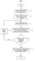
- Fig. 1 is an exemplary flowchart illustrating the method of applying assist features to a mask pattern in accordance with a first embodiment of the present invention.
- the first step (Step 10) in the process is to identify the target mask pattern and illumination system and settings to be utilized to image the pattern.
- An exemplary target pattern comprising contact holes 210 is shown in Fig. 2a.
- the next step (Step 12) in the process is to determine the optimal focus setting for imaging the target pattern utilizing the given imaging system. As is known, the optimum focus setting can be determined either by a calibration or simulation process.
- the next step in the process (Step 14) is to generate an interference map (IM) for the target pattern utilizing the optimum focus setting.
- the interference map can be generated in the manner disclosed in USP App. Ser.
- the interference map is utilized to determine the optimal seeding sites for the assist features relative to each of the features in the target pattern (Step 16) for the given focus setting.
- the optimal seed site for the assist feature at the optimal focus condition is indicated by location "1" (which as noted above is determined by analyzing the interference map). It is noted that while the example illustrated in Fig. 2b only depicts the foregoing process being applied to a single contact hole, in an actual implementation the assist features would be disposed adjacent to numerous contact holes.
- the next step in the process is to vary the defocus setting, recompute the interference map for new defocus setting and determine the optimal seeding sites for the assist features for the new defocus setting.
- the resulting interference map will change as the defocus setting changes, and therefore the optimal placement of the assist feature changes as the defocus setting changes.
- the number of defocus settings for which an interference map should be calculated is a minimum of two. However, if a greater the number of defocus settings are considered, a more optimal result may be obtained. Typically, three or four defocus settings would be considered adequate.
- the variation between the defocus setting is determined, for example, in accordance with the NA of the imaging system being utilized.
- Step 18 it is determined if an interference map needs to be generated for another defocus setting. If yes, the process proceeds to Step 20, where the defocus setting is adjusted, and then the process proceeds back to Step 14, where the interference map is recomputed utilizing the new defocus setting. The process then proceeds again to Step 16 where the optimal seeding sites for the assist features for the new defocus setting is determined. This loop is repeated until all of the defocus settings are processed.
- location “1" represents the seeding site for the assist feature for contact "X” at best focus (i.e., defocus equals 0 um).
- Location “2" represents the seeding site for the assist feature for contact "X” at a first defocus (i.e., defocus equals 0.075 um).
- Location “3" represents the seeding site for the assist feature for contact "X” at a second defocus (i.e., defocus equals 0.150 um).
- Location "4" represents the seeding site for the assist feature for contact "X” at a third defocus (i.e., defocus equals 0.225 um).
- the next step (Step 22) in the process is to formed an assist feature encompassing each of the seeding sites identified for each of the defocus conditions.
- This result assist feature represents the assist feature to be utilized in the actual mask design.
- the assist feature is created by forming small square assist features 220 around each seeding site identified in the foregoing process. The small squares 220 are then grouped together to form one assist feature 230 as shown in Fig. 2d. It is noted that the finer the increments when varying the defocus settings, the resulting assist feature will exhibit less of a stair-step shape.
- the given embodiment illustrates the assist feature being formed by a group of square features, it is possible to utilize any type of shape to form the final assist feature, with the restriction being that the all of the seeding sites should be encompassed by the assist feature and the assist feature must remain sub-resolution.
- Fig. 3 illustrates an actual example of the result of utilizing the foregoing process to place assist features within a mask pattern.
- elements 320 represent SBs (i.e., assist features) formed to encompass a group of seeding sites in the manner set forth above
- elements 340 represent the intended contact holes
- elements 360 represent the intended contact holes modified/treated with OPC.
- assist features in either one of or both constructive areas of interference or destructive areas of interference.
- assist feature would be formed so as to have the same phase relative to the contact hole to be imaged, whereas for placement of assist features in areas of destructive interference, the assist feature would be formed so as to have a ⁇ -phase shift relative to the contact hole to be imaged. Both types of assist features are shown in Fig. 3.
- a process for optimizing the size and shape of the assist features disposed in the target pattern.
- it is desirable to form the assist features as large as possible.
- larger assist feature dimensions result in an easier mask manufacturing process.
- the assist feature must not be printable under nominal printing conditions for the CD target features.
- Known prior art methods typically utilized a traditional rule-based approach to define the size of the assist feature, where X & Y size limits where predefined.
- a model-based method for maximizing the size and shape of the assist features within the target pattern. More specifically, utilizing an aerial image analysis each of the assist features is grown until the assist feature reaches a predefined threshold, which is some percentage less than the printing threshold for the given imaging system and process being utilized.
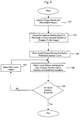
- Fig. 4 illustrates an exemplary flowchart illustrating the method of growing the assist features in accordance with the second embodiment of the present invention.
- the first step (Step 410) in the process is to define the target pattern and the illumination system to be utilized.
- the next step (Step 420) in the process is to determine the optimal seeding sites for the assist features relative to the features to be imaged.
- Step 420 can be performed utilizing the process disclosed in the first embodiment of the present invention discussed above. However, it is noted that Step 420 can also be performed utilizing the seeding site identification process disclosed in USP Application Ser. No. 10/756,830.
- the next step (Step 430) is to form an assist feature around the seeding sites so that the assist features have a size which is below the predefined threshold.
- the predefined threshold represents the maximum intensity that any assist feature may have so as to insure that the assist feature will not image on the wafer.
- the predefined threshold is set at some percentage below the printing threshold for the CD of the target feature. For example, if the nominal printing threshold for the CD target feature is 0.3 (with respect to open-frame exposure intensity), the maximum intensity for assist features (i.e., the predefined threshold) can be set at 0.15, which is well below the printing threshold.
- the predefined threshold utilized in this process is dependent on the imaging system being utilized and the dimensions of the features to be imaged.
- assist features are positioned about the seeding sites, and the assist features are sized so as to have an initial dimension that results in a corresponding image intensity that is less than the predefined threshold.
- image intensity of the assist features can be determined utilizing known OPC simulation systems such as MaskWeaver TM , offered for sale by ASML MaskTools, Inc.
- the next step in the process is to select a first assist feature and increase the size of the assist feature until the image intensity of the given assist feature reaches the predefined threshold.
- the size of the given assist feature corresponding to the image intensity equaling the predefined threshold defines the size of the given assist feature to be utilized in the mask.
- the process proceeds to the next assist feature, and increases the size of this assist feature until the image intensity associated with this assist feature equals the predefined threshold. This process is continued until all of the assist features placed in the mask pattern in Step 430 have been processed.
- This loop is represented by Steps 440, 450 and 460 as shown in Fig. 4. It is noted that the assist features that are more sensitive (i.e., likely to print) will reach the predefined intensity faster than those assist features that are less sensitive, and therefore will have a smaller size relative to the less sensitive assist features in the final mask pattern.
- the assist features are increased in size utilizing the following process.
- the size of the assist featured is increased in the X direction and the image intensity is monitored.
- the image intensity of the given assist feature can be monitored utilizing OPC simulation software.
- the size is increased in the X-direction until the X-limit is reached.
- the assist feature is then grown in the Y-direction.
- the size of the assist feature is increased in the Y-direction until the Y-limit is reached.
- the X-limit and Y-limit are also governed by the amount of space between the target pattern in the design and the minimum distance required between a target pattern and a sub-resolution assist feature.
- the objective is to maximize both the growth in X-direction and the Y-direction but never allow the overall assist feature size and shape to produce the intensity that is exceeding the predefined threshold limit.
- the foregoing example illustrates the assist feature being first grown in the X-direction and then grown in the Y-direction, the present invention is not limited to this process. In a variation of the foregoing, it would be possible to first grow the assist feature in the Y-direction, followed by growth in the X-direction, or alternatively, grow both the X and Y dimensions of the assist feature simultaneously.
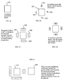
- Figs. 5a-5d illustrate the foregoing process of growing the assist features. More specifically, Fig. 5a illustrates an exemplary contact hole 510 for which assist features will be generated to improve imaging (corresponding to Step 410). Fig. 5b illustrates the seeding sites 520 for placement of assist features determined from the interference map in the manner set forth above (Step 420). Fig. 5c illustrates the initial assist features 540 placed around the seeding sites (Step 430). Fig. 5d illustrates the assist features grown to the maximum size allowable.
- Fig. 6 illustrates how an adjacent feature can effect (in this instance limit) the growth of a given assist feature.
- a second contact hole 610 is added to the pattern shown in Fig. 5a.
- the growth of the assist feature 620 disposed between the first contact hole 510 and the second contact hole 610 is limited.
- the interference map is utilized to determine whether the given features in the target pattern represent strong or weak features with respect to imaging performance. More specifically, the interference map is analyzed to determine the intensity of the interference at the locations of the features within the mask. Features located at positions having high levels of interference are considered strong features that will image easily. Alternatively, features located at positions exhibiting reduced levels of interference may exhibit unacceptable imaging results. Once defined, as explained in detail below, additional steps can be taken to ensure acceptable printing of the weak features.
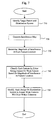
- Fig. 7 illustrates a flowchart describing the method of defining features to be imaged as either a weak feature or a string feature with respect to the imaging process.
- the first step (Step 710) is to define the target pattern and the illumination system to be utilized.
- the next step (Step 720) in the process is to generate an interference map for the target pattern based on the imaging system and process to be utilized. Thereafter, the interference map is utilized to determine the magnitude of interference at each feature location (Step 730).
- each feature to be imaged is defined as either a weak feature or a strong feature based on whether or not the magnitude of interference at the given feature location is above or below a predefined interference value.
- Those features having an interference magnitude which is greater than the predefined interference value are defined as strong features (and represent features that will print easily), while the features having an interference magnitude less than the predefined interference value are defined as weak features (are represent features that will have difficulty printing). It is noted that the predefined interference value, which is utilized to define whether or not a feature is a strong interference feature or a weak interference feature, can be determined utilizing a process window simulation.
- the interference map of the target pattern exhibits an interference magnitude ranging from 1.0 to 0.7 at the feature locations (where the magnitudes of interference have been normalized to 1.0)
- the simulation program such as LithoCruiserTM, sold by ASML MaskTools, Inc.
- features having an interference magnitude greater than 0.8 are defined as strong features
- features having an interference magnitude below 0.8 are defined as weak features.
- additional measures can be taken to ensure that the weak features will print within the process tolerance requirements (Step 750).
- additional measures include, but are not limited to, adjusting the illumination and NA setting; varying the location and/or shape of the weak features within the target pattern; or separating the weak features and the strong features into two separate exposure masks.
- Figs. 8a and 8b illustrate the use of the interference map for identifying weak and strong features.
- Fig. 8a illustrates a partial interference map for a given NA and illumination setting.
- the two outside features 810 and 820 are strong features that will image easily
- the middle feature 830 is a weak feature relative to the two outside features. As such, the middle feature may not image properly.
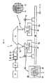
- Fig. 9 schematically depicts a lithographic projection apparatus suitable for use with a mask designed with the aid of the current invention.
- the apparatus comprises:
- the apparatus is of a transmissive type (i.e ., has a transmissive mask). However, in general, it may also be of a reflective type, for example (with a reflective mask). Alternatively, the apparatus may employ another kind of patterning means as an alternative to the use of a mask; examples include a programmable mirror array or LCD matrix.
- the source LA e.g ., a mercury lamp or excimer laser
- This beam is fed into an illumination system (illuminator) IL, either directly or after having traversed conditioning means, such as a beam expander Ex, for example.
- the illuminator IL may comprise adjusting means AM for setting the outer and/or inner radial extent (commonly referred to as ⁇ -outer and ⁇ -inner, respectively) of the intensity distribution in the beam.
- ⁇ -outer and ⁇ -inner commonly referred to as ⁇ -outer and ⁇ -inner, respectively
- it will generally comprise various other components, such as an integrator IN and a condenser CO.
- the beam PB impinging on the mask MA has a desired uniformity and intensity distribution in its cross-section.
- the source LA may be within the housing of the lithographic projection apparatus (as is often the case when the source LA is a mercury lamp, for example), but that it may also be remote from the lithographic projection apparatus, the radiation beam that it produces being led into the apparatus (e.g., with the aid of suitable directing mirrors); this latter scenario is often the case when the source LA is an excimer laser (e.g., based on KrF, ArF or F 2 lasing).
- the current invention encompasses both of these scenarios.
- the beam PB subsequently intercepts the mask MA, which is held on a mask table MT. Having traversed the mask MA, the beam PB passes through the lens PL, which focuses the beam PB onto a target portion C of the substrate W. With the aid of the second positioning means (and interferometric measuring means IF), the substrate table WT can be moved accurately, e.g ., so as to position different target portions C in the path of the beam PB. Similarly, the first positioning means can be used to accurately position the mask MA with respect to the path of the beam PB, e.g ., after mechanical retrieval of the mask MA from a mask library, or during a scan.
- the mask table MT may just be connected to a short-stroke actuator, or may be fixed.
- the depicted tool can be used in two different modes:
- software may implement or aid in performing the disclosed concepts.
- Software functionalities of a computer system involve programming, including executable code, may be used to implement the above described imaging model.
- the software code is executable by the general-purpose computer.
- the code, and possibly the associated data records are stored within a general-purpose computer platform.
- the software may be stored at other locations and/or transported for loading into the appropriate general-purpose computer systems.
- the embodiments discussed above involve one or more software products in the form of one or more modules of code carried by at least one machine-readable medium. Execution of such code by a processor of the computer system enables the platform to implement the catalog and/or software downloading functions in essentially the manner performed in the embodiments discussed and illustrated herein.
- Non-volatile media include, for example, optical or magnetic disks, such as any of the storage devices in any computer(s) operating as one of the server platforms discussed above.
- Volatile media include dynamic memory, such as main memory of such a computer platform.
- Physical transmission media include coaxial cables, copper wire and fiber optics, including the wires that comprise a bus within a computer system.
- Carrier-wave transmission media can take the form of electric or electromagnetic signals, or acoustic or light waves such as those generated during radio frequency (RF) and infrared (IR) data communications.
- Common forms of computer-readable media therefore include, for example: a floppy disk, a flexible disk, hard disk, magnetic tape, any other magnetic medium, a CD-ROM, DVD, any other optical medium, less commonly used media such as punch cards, paper tape, any other physical medium with patterns of holes, a RAM, a PROM, and EPROM, a FLASH-EPROM, any other memory chip or cartridge, a carrier wave transporting data or instructions, cables or links transporting such a carrier wave, or any other medium from which a computer can read programming code and/or data.
- Many of these forms of computer readable media may be involved in carrying one or more sequences of one or more instructions to a processor for execution.
Landscapes
- Physics & Mathematics (AREA)
- General Physics & Mathematics (AREA)
- Exposure And Positioning Against Photoresist Photosensitive Materials (AREA)
- Preparing Plates And Mask In Photomechanical Process (AREA)
- Exposure Of Semiconductors, Excluding Electron Or Ion Beam Exposure (AREA)
Applications Claiming Priority (1)
| Application Number | Priority Date | Filing Date | Title |
|---|---|---|---|
| US60356004P | 2004-08-24 | 2004-08-24 |
Publications (2)
| Publication Number | Publication Date |
|---|---|
| EP1630601A2 true EP1630601A2 (de) | 2006-03-01 |
| EP1630601A3 EP1630601A3 (de) | 2008-07-02 |
Family
ID=35431328
Family Applications (1)
| Application Number | Title | Priority Date | Filing Date |
|---|---|---|---|
| EP05255190A Withdrawn EP1630601A3 (de) | 2004-08-24 | 2005-08-24 | Maskenherstellungsverfahren, Verfahren zur optischen Naheffektkorrektur (OPC), Verfahren zur Herstellung einer Vorrichtung, Computerprogramm und computerlesbares Speichermedium |
Country Status (7)
| Country | Link |
|---|---|
| US (2) | US7620930B2 (de) |
| EP (1) | EP1630601A3 (de) |
| JP (1) | JP4383400B2 (de) |
| KR (1) | KR100860328B1 (de) |
| CN (1) | CN100543588C (de) |
| SG (1) | SG120284A1 (de) |
| TW (1) | TWI370955B (de) |
Cited By (2)
| Publication number | Priority date | Publication date | Assignee | Title |
|---|---|---|---|---|
| CN101359178B (zh) * | 2007-08-03 | 2011-06-01 | 中芯国际集成电路制造(上海)有限公司 | 光学邻近校正的方法 |
| CN104423172A (zh) * | 2013-08-27 | 2015-03-18 | 中芯国际集成电路制造(北京)有限公司 | 一种散射条模拟成像的检测方法 |
Families Citing this family (29)
| Publication number | Priority date | Publication date | Assignee | Title |
|---|---|---|---|---|
| US7620930B2 (en) * | 2004-08-24 | 2009-11-17 | Asml Masktools B.V. | Method, program product and apparatus for model based scattering bar placement for enhanced depth of focus in quarter-wavelength lithography |
| US7509621B2 (en) * | 2005-01-03 | 2009-03-24 | Synopsys, Inc. | Method and apparatus for placing assist features by identifying locations of constructive and destructive interference |
| US7424699B2 (en) * | 2005-06-10 | 2008-09-09 | Texas Instruments Incorporated | Modifying sub-resolution assist features according to rule-based and model-based techniques |
| US8132130B2 (en) * | 2005-06-22 | 2012-03-06 | Asml Masktools B.V. | Method, program product and apparatus for performing mask feature pitch decomposition for use in a multiple exposure process |
| EP1804119A1 (de) * | 2005-12-27 | 2007-07-04 | Interuniversitair Microelektronica Centrum | Verfahren zur Herstellung gedämpfter Phasenverschiebungsmasken und daraus erhaltene Vorrichtungen |
| US20070226674A1 (en) * | 2006-03-27 | 2007-09-27 | Henning Haffner | System and method for semiconductor device fabrication using modeling |
| US7548315B2 (en) * | 2006-07-27 | 2009-06-16 | Asml Netherlands B.V. | System and method to compensate for critical dimension non-uniformity in a lithography system |
| US8341561B2 (en) * | 2006-12-12 | 2012-12-25 | Samsung Electronics Co., Ltd. | Methods of arranging mask patterns and associated apparatus |
| KR100874913B1 (ko) * | 2006-12-12 | 2008-12-19 | 삼성전자주식회사 | 마스크 패턴을 배치하는 방법 및 이를 이용한 장치 |
| KR100881184B1 (ko) * | 2006-12-12 | 2009-02-05 | 삼성전자주식회사 | 마스크 패턴을 배치하는 방법 및 이를 이용한 장치 |
| US20080169510A1 (en) * | 2007-01-17 | 2008-07-17 | International Business Machines Corporation | Performance enhancement on both nmosfet and pmosfet using self-aligned dual stressed films |
| KR101096145B1 (ko) * | 2007-06-04 | 2011-12-19 | 에이에스엠엘 네델란즈 비.브이. | 모델-기반 리소그래피 안내 레이아웃 설계를 수행하는 방법들 |
| KR101317844B1 (ko) * | 2007-07-06 | 2013-10-11 | 삼성전자주식회사 | 마스크 패턴을 배치하는 방법 및 이를 이용한 장치 |
| US9779186B2 (en) | 2007-08-28 | 2017-10-03 | Asml Netherlands B.V. | Methods for performing model-based lithography guided layout design |
| US8028252B2 (en) * | 2007-09-14 | 2011-09-27 | Luminescent Technologies Inc. | Technique for determining mask patterns and write patterns |
| JP2009093138A (ja) * | 2007-09-19 | 2009-04-30 | Canon Inc | 原版データの生成方法、原版作成方法、露光方法、デバイス製造方法及び原版データを作成するためのプログラム |
| EP2040120B1 (de) * | 2007-09-19 | 2011-03-02 | Canon Kabushiki Kaisha | Maskendatenerzeugungsverfahren, Maskenherstellungsverfahren, Belichtungsverfahren, Vorrichtungsherstellungsverfahren und Programm |
| KR101113326B1 (ko) * | 2009-07-01 | 2012-03-13 | 주식회사 하이닉스반도체 | 포토마스크의 보조패턴 형성방법 |
| US8250498B2 (en) * | 2010-01-28 | 2012-08-21 | Synopsys, Inc. | Method and apparatus for calibrating a photolithography process model by using a process window parameter |
| JP5279745B2 (ja) | 2010-02-24 | 2013-09-04 | 株式会社東芝 | マスクレイアウト作成方法、マスクレイアウト作成装置、リソグラフィ用マスクの製造方法、半導体装置の製造方法、およびコンピュータが実行可能なプログラム |
| KR101991380B1 (ko) | 2012-07-26 | 2019-06-20 | 삼성전자주식회사 | 반도체 소자의 레이아웃 생성 방법 |
| US9310674B2 (en) | 2014-02-20 | 2016-04-12 | International Business Machines Corporation | Mask that provides improved focus control using orthogonal edges |
| US9805154B2 (en) * | 2015-05-15 | 2017-10-31 | Taiwan Semiconductor Manufacturing Company, Ltd. | Method of lithography process with inserting scattering bars |
| JP2017090817A (ja) * | 2015-11-16 | 2017-05-25 | キヤノン株式会社 | 露光装置、及び物品の製造方法 |
| US10176966B1 (en) | 2017-04-13 | 2019-01-08 | Fractilia, Llc | Edge detection system |
| US10522322B2 (en) | 2017-04-13 | 2019-12-31 | Fractilia, Llc | System and method for generating and analyzing roughness measurements |
| US10262100B2 (en) * | 2017-05-24 | 2019-04-16 | Synopsys, Inc. | Rule based assist feature placement using skeletons |
| KR20210133364A (ko) | 2020-04-28 | 2021-11-08 | 삼성전자주식회사 | 반도체 장치의 제조를 위한 방법 및 컴퓨팅 장치 |
| CN113589644A (zh) * | 2021-07-15 | 2021-11-02 | 中国科学院上海光学精密机械研究所 | 基于亚分辨率辅助图形种子插入的曲线型逆向光刻方法 |
Citations (2)
| Publication number | Priority date | Publication date | Assignee | Title |
|---|---|---|---|---|
| EP1439420A1 (de) * | 2003-01-14 | 2004-07-21 | ASML Masktools B.V. | Rechnergestütztes optisches Näherungskorrekturverfahren für Kontaktlochmasken |
| EP1439419A2 (de) * | 2003-01-14 | 2004-07-21 | ASML Masktools B.V. | Methode und Gerät zur Erstellung von optischen Näherungseffekt-Korrekturelementen für ein Maskenmuster in der Optischen Lithographie |
Family Cites Families (30)
| Publication number | Priority date | Publication date | Assignee | Title |
|---|---|---|---|---|
| JPH04216548A (ja) * | 1990-12-18 | 1992-08-06 | Mitsubishi Electric Corp | フォトマスク |
| US5242770A (en) * | 1992-01-16 | 1993-09-07 | Microunity Systems Engineering, Inc. | Mask for photolithography |
| US5447810A (en) * | 1994-02-09 | 1995-09-05 | Microunity Systems Engineering, Inc. | Masks for improved lithographic patterning for off-axis illumination lithography |
| KR960002536A (de) * | 1994-06-29 | 1996-01-26 | ||
| US5682323A (en) * | 1995-03-06 | 1997-10-28 | Lsi Logic Corporation | System and method for performing optical proximity correction on macrocell libraries |
| US5705301A (en) * | 1996-02-27 | 1998-01-06 | Lsi Logic Corporation | Performing optical proximity correction with the aid of design rule checkers |
| JP4075966B2 (ja) * | 1996-03-06 | 2008-04-16 | エーエスエムエル ネザーランズ ビー.ブイ. | 差分干渉計システム及びこのシステムを具えたリソグラフステップアンドスキャン装置 |
| EP0890136B9 (de) * | 1996-12-24 | 2003-12-10 | ASML Netherlands B.V. | In zwei richtungen ausgewogenes positioniergerät, sowie lithographisches gerät mit einem solchen positioniergerät |
| US6223139B1 (en) * | 1998-09-15 | 2001-04-24 | International Business Machines Corporation | Kernel-based fast aerial image computation for a large scale design of integrated circuit patterns |
| JP3275863B2 (ja) * | 1999-01-08 | 2002-04-22 | 日本電気株式会社 | フォトマスク |
| US6214497B1 (en) * | 1999-06-29 | 2001-04-10 | Micron Technology, Inc. | Method to eliminate side lobe printing of attenuated phase shift masks |
| US6303253B1 (en) * | 2000-03-16 | 2001-10-16 | International Business Machines Corporation | Hierarchy and domain-balancing method and algorithm for serif mask design in microlithography |
| US6503666B1 (en) | 2000-07-05 | 2003-01-07 | Numerical Technologies, Inc. | Phase shift masking for complex patterns |
| US6777141B2 (en) * | 2000-07-05 | 2004-08-17 | Numerical Technologies, Inc. | Phase shift mask including sub-resolution assist features for isolated spaces |
| US6787271B2 (en) * | 2000-07-05 | 2004-09-07 | Numerical Technologies, Inc. | Design and layout of phase shifting photolithographic masks |
| TW552561B (en) | 2000-09-12 | 2003-09-11 | Asml Masktools Bv | Method and apparatus for fast aerial image simulation |
| US6901575B2 (en) * | 2000-10-25 | 2005-05-31 | Numerical Technologies, Inc. | Resolving phase-shift conflicts in layouts using weighted links between phase shifters |
| TWI285295B (en) | 2001-02-23 | 2007-08-11 | Asml Netherlands Bv | Illumination optimization in lithography |
| US6519760B2 (en) | 2001-02-28 | 2003-02-11 | Asml Masktools, B.V. | Method and apparatus for minimizing optical proximity effects |
| US6792591B2 (en) * | 2001-02-28 | 2004-09-14 | Asml Masktools B.V. | Method of identifying an extreme interaction pitch region, methods of designing mask patterns and manufacturing masks, device manufacturing methods and computer programs |
| US6703167B2 (en) * | 2001-04-18 | 2004-03-09 | Lacour Patrick Joseph | Prioritizing the application of resolution enhancement techniques |
| US6749970B2 (en) | 2001-12-11 | 2004-06-15 | Advanced Micro Devices, Inc. | Method of enhancing clear field phase shift masks with border regions around phase 0 and phase 180 regions |
| US7023528B2 (en) * | 2002-06-10 | 2006-04-04 | International Business Machines Corporation | Hybrid electronic mask |
| US6807662B2 (en) * | 2002-07-09 | 2004-10-19 | Mentor Graphics Corporation | Performance of integrated circuit components via a multiple exposure technique |
| WO2004008244A2 (en) | 2002-07-15 | 2004-01-22 | Kla-Tencor Technologies Corp. | Defect inspection methods that include acquiring aerial images of a reticle for different lithographic process variables |
| US7266480B2 (en) * | 2002-10-01 | 2007-09-04 | The Regents Of The University Of California | Rapid scattering simulation of objects in imaging using edge domain decomposition |
| US7376930B2 (en) * | 2003-06-30 | 2008-05-20 | Asml Masktools B.V. | Method, program product and apparatus for generating assist features utilizing an image field map |
| EP1513012B1 (de) * | 2003-09-05 | 2008-02-20 | ASML MaskTools B.V. | Methode und Vorrichtung für modellgestützte Plazierung phasenbalancierter Hilfsstrukturen für optische Lithographie mit Auflösungsgrenzen unterhalb der Belichtungswellenlänge |
| US7232630B2 (en) * | 2003-12-11 | 2007-06-19 | Synopsys, Inc | Method for printability enhancement of complementary masks |
| US7620930B2 (en) * | 2004-08-24 | 2009-11-17 | Asml Masktools B.V. | Method, program product and apparatus for model based scattering bar placement for enhanced depth of focus in quarter-wavelength lithography |
-
2005
- 2005-08-22 US US11/208,015 patent/US7620930B2/en active Active
- 2005-08-23 SG SG200505331A patent/SG120284A1/en unknown
- 2005-08-23 JP JP2005272697A patent/JP4383400B2/ja not_active Expired - Fee Related
- 2005-08-24 CN CNB2005101165341A patent/CN100543588C/zh not_active Expired - Fee Related
- 2005-08-24 EP EP05255190A patent/EP1630601A3/de not_active Withdrawn
- 2005-08-24 KR KR1020050077709A patent/KR100860328B1/ko active IP Right Grant
- 2005-08-24 TW TW094128950A patent/TWI370955B/zh not_active IP Right Cessation
-
2009
- 2009-11-05 US US12/613,344 patent/US8495529B2/en active Active
Patent Citations (2)
| Publication number | Priority date | Publication date | Assignee | Title |
|---|---|---|---|---|
| EP1439420A1 (de) * | 2003-01-14 | 2004-07-21 | ASML Masktools B.V. | Rechnergestütztes optisches Näherungskorrekturverfahren für Kontaktlochmasken |
| EP1439419A2 (de) * | 2003-01-14 | 2004-07-21 | ASML Masktools B.V. | Methode und Gerät zur Erstellung von optischen Näherungseffekt-Korrekturelementen für ein Maskenmuster in der Optischen Lithographie |
Non-Patent Citations (3)
| Title |
|---|
| BROEKE VAN DEN D ET AL: "APPLICATION OF CPL WITH INTERFERENCE MAPPING LITHOGRAPHY TO GENERATE RANDOM CONTACT RETICLE DESIGNS FOR THE 65NM NODE" PROCEEDINGS OF THE SPIE, SPIE, BELLINGHAM, VA, US, vol. 5446, no. 1, 14 April 2004 (2004-04-14), pages 550-559, XP002352892 ISSN: 0277-786X * |
| BROEKE VAN DEN D ET AL: "Near 0.3 k1 full pitch range contact hole patterning using Chromeless Phase Lithography (CPL)" PROCEEDINGS OF THE SPIE, SPIE, BELLINGHAM, VA, US, vol. 5256, 9 September 2003 (2003-09-09), pages 297-308, XP002353565 ISSN: 0277-786X * |
| TOUBLAN O ET AL: "Fully automatic side lobe detection and correction technique for attenuated phase shift masks" PROCEEDINGS OF THE SPIE, SPIE, BELLINGHAM, VA, US, vol. 4346, no. PART 1-2, 2001, pages 1541-1547, XP002276634 ISSN: 0277-786X * |
Cited By (2)
| Publication number | Priority date | Publication date | Assignee | Title |
|---|---|---|---|---|
| CN101359178B (zh) * | 2007-08-03 | 2011-06-01 | 中芯国际集成电路制造(上海)有限公司 | 光学邻近校正的方法 |
| CN104423172A (zh) * | 2013-08-27 | 2015-03-18 | 中芯国际集成电路制造(北京)有限公司 | 一种散射条模拟成像的检测方法 |
Also Published As
| Publication number | Publication date |
|---|---|
| CN100543588C (zh) | 2009-09-23 |
| US7620930B2 (en) | 2009-11-17 |
| US20060075377A1 (en) | 2006-04-06 |
| US20100047699A1 (en) | 2010-02-25 |
| US8495529B2 (en) | 2013-07-23 |
| KR100860328B1 (ko) | 2008-09-25 |
| KR20060050603A (ko) | 2006-05-19 |
| TW200619863A (en) | 2006-06-16 |
| CN1800987A (zh) | 2006-07-12 |
| JP2006065338A (ja) | 2006-03-09 |
| TWI370955B (en) | 2012-08-21 |
| SG120284A1 (en) | 2006-03-28 |
| JP4383400B2 (ja) | 2009-12-16 |
| EP1630601A3 (de) | 2008-07-02 |
Similar Documents
| Publication | Publication Date | Title |
|---|---|---|
| US7620930B2 (en) | Method, program product and apparatus for model based scattering bar placement for enhanced depth of focus in quarter-wavelength lithography | |
| US7594199B2 (en) | Method of optical proximity correction design for contact hole mask | |
| US7681171B2 (en) | Method, program product and apparatus for performing double exposure lithography | |
| US7349066B2 (en) | Apparatus, method and computer program product for performing a model based optical proximity correction factoring neighbor influence | |
| US7138212B2 (en) | Method and apparatus for performing model-based layout conversion for use with dipole illumination | |
| US7493589B2 (en) | Method, program product and apparatus for model based geometry decomposition for use in a multiple exposure process | |
| US7550235B2 (en) | Method and apparatus for performing model based placement of phase-balanced scattering bars for sub-wavelength optical lithography | |
| US7376930B2 (en) | Method, program product and apparatus for generating assist features utilizing an image field map | |
| EP1528429A2 (de) | Optimierung von Strukturen auf Photomasken mittels Simulation des projezierten Musters | |
| JP2003162042A (ja) | ダイポール式照明技術に関連して使用されるマスクの生成方法と生成装置 | |
| JP2004133426A (ja) | 自動光近接補正(opc)ルール作成 | |
| US7514183B2 (en) | Method for performing transmission tuning of a mask pattern to improve process latitude | |
| US7804646B2 (en) | Method for decomposition of a customized DOE for use with a single exposure into a set of multiple exposures using standard DOEs with optimized exposure settings | |
| US7614034B2 (en) | Method and apparatus for generating OPC rules for placement of scattering bar features utilizing interface mapping technology |
Legal Events
| Date | Code | Title | Description |
|---|---|---|---|
| PUAI | Public reference made under article 153(3) epc to a published international application that has entered the european phase |
Free format text: ORIGINAL CODE: 0009012 |
|
| AK | Designated contracting states |
Kind code of ref document: A2 Designated state(s): AT BE BG CH CY CZ DE DK EE ES FI FR GB GR HU IE IS IT LI LT LU LV MC NL PL PT RO SE SI SK TR |
|
| AX | Request for extension of the european patent |
Extension state: AL BA HR MK YU |
|
| RIC1 | Information provided on ipc code assigned before grant |
Ipc: G03F 7/20 20060101ALI20080310BHEP Ipc: G03F 1/14 20060101AFI20051209BHEP |
|
| PUAL | Search report despatched |
Free format text: ORIGINAL CODE: 0009013 |
|
| AK | Designated contracting states |
Kind code of ref document: A3 Designated state(s): AT BE BG CH CY CZ DE DK EE ES FI FR GB GR HU IE IS IT LI LT LU LV MC NL PL PT RO SE SI SK TR |
|
| AX | Request for extension of the european patent |
Extension state: AL BA HR MK YU |
|
| 17P | Request for examination filed |
Effective date: 20080922 |
|
| 17Q | First examination report despatched |
Effective date: 20081107 |
|
| AKX | Designation fees paid |
Designated state(s): DE FR GB IT NL |
|
| STAA | Information on the status of an ep patent application or granted ep patent |
Free format text: STATUS: THE APPLICATION IS DEEMED TO BE WITHDRAWN |
|
| 18D | Application deemed to be withdrawn |
Effective date: 20090519 |