EP1623431B1 - A non-volatile memory having a bias on the source electrode for hci programming - Google Patents
A non-volatile memory having a bias on the source electrode for hci programming Download PDFInfo
- Publication number
- EP1623431B1 EP1623431B1 EP04760554A EP04760554A EP1623431B1 EP 1623431 B1 EP1623431 B1 EP 1623431B1 EP 04760554 A EP04760554 A EP 04760554A EP 04760554 A EP04760554 A EP 04760554A EP 1623431 B1 EP1623431 B1 EP 1623431B1
- Authority
- EP
- European Patent Office
- Prior art keywords
- source
- circuit
- memory
- programming
- memory cell
- Prior art date
- Legal status (The legal status is an assumption and is not a legal conclusion. Google has not performed a legal analysis and makes no representation as to the accuracy of the status listed.)
- Expired - Lifetime
Links
- 230000015654 memory Effects 0.000 title claims abstract description 73
- 238000000034 method Methods 0.000 claims description 20
- 230000008878 coupling Effects 0.000 claims description 3
- 238000010168 coupling process Methods 0.000 claims description 3
- 238000005859 coupling reaction Methods 0.000 claims description 3
- 238000013459 approach Methods 0.000 abstract description 5
- 239000000872 buffer Substances 0.000 description 10
- 230000008901 benefit Effects 0.000 description 8
- 230000000694 effects Effects 0.000 description 6
- 230000008569 process Effects 0.000 description 5
- 238000012360 testing method Methods 0.000 description 4
- 238000010586 diagram Methods 0.000 description 3
- 238000007667 floating Methods 0.000 description 3
- 238000002347 injection Methods 0.000 description 3
- 239000007924 injection Substances 0.000 description 3
- 239000004065 semiconductor Substances 0.000 description 3
- 239000000243 solution Substances 0.000 description 3
- 238000012986 modification Methods 0.000 description 2
- 230000004048 modification Effects 0.000 description 2
- 230000003071 parasitic effect Effects 0.000 description 2
- 230000004044 response Effects 0.000 description 2
- 230000002411 adverse Effects 0.000 description 1
- 230000002950 deficient Effects 0.000 description 1
- 239000003989 dielectric material Substances 0.000 description 1
- 230000003028 elevating effect Effects 0.000 description 1
- 238000005516 engineering process Methods 0.000 description 1
- 239000002784 hot electron Substances 0.000 description 1
- 239000011159 matrix material Substances 0.000 description 1
- 239000002159 nanocrystal Substances 0.000 description 1
- 150000004767 nitrides Chemical class 0.000 description 1
- 238000012545 processing Methods 0.000 description 1
- 239000011232 storage material Substances 0.000 description 1
- 239000000758 substrate Substances 0.000 description 1
Images
Classifications
-
- G—PHYSICS
- G11—INFORMATION STORAGE
- G11C—STATIC STORES
- G11C16/00—Erasable programmable read-only memories
- G11C16/02—Erasable programmable read-only memories electrically programmable
- G11C16/06—Auxiliary circuits, e.g. for writing into memory
- G11C16/10—Programming or data input circuits
- G11C16/12—Programming voltage switching circuits
-
- G—PHYSICS
- G11—INFORMATION STORAGE
- G11C—STATIC STORES
- G11C16/00—Erasable programmable read-only memories
- G11C16/02—Erasable programmable read-only memories electrically programmable
- G11C16/06—Auxiliary circuits, e.g. for writing into memory
- G11C16/10—Programming or data input circuits
-
- G—PHYSICS
- G11—INFORMATION STORAGE
- G11C—STATIC STORES
- G11C11/00—Digital stores characterised by the use of particular electric or magnetic storage elements; Storage elements therefor
- G11C11/21—Digital stores characterised by the use of particular electric or magnetic storage elements; Storage elements therefor using electric elements
- G11C11/34—Digital stores characterised by the use of particular electric or magnetic storage elements; Storage elements therefor using electric elements using semiconductor devices
-
- G—PHYSICS
- G11—INFORMATION STORAGE
- G11C—STATIC STORES
- G11C16/00—Erasable programmable read-only memories
- G11C16/02—Erasable programmable read-only memories electrically programmable
- G11C16/06—Auxiliary circuits, e.g. for writing into memory
- G11C16/30—Power supply circuits
Definitions
- This invention relates to non-volatile semiconductor memories, and more particularly, to non-volatile semiconductor memories that have a bias applied to the source electrodes of the memory array cells of the memory.
- Non-volatile memories are typically programmed using hot carrier injection (HCI) because it is significantly faster than the alternatives.
- HCI hot carrier injection
- An important aspect of HCI is that electrons are energized by current flow and that some of these electrons are sufficiently energized to jump to the storage layer that is above the channel where the current is flowing.
- programming is faster if there is more current (for a given field) and faster if a higher percentage of the electrons (for a given current) are sufficiently energized to reach the storage layer.
- a lower drain to source voltage has the doubly bad effect of both reducing current and reducing the percentage of electrons that have this sufficient energy. This can come about by deselected memory transistors that have too low of a threshold voltage and are conductive during programming of other cells in the same column.
- the programming voltage is generally provided by a power supply with limited capability, that is, one that has a fairly high output impedance. Thus, drawing relatively large currents can have the effect of loading down the supply to the point where the supply voltage is significantly reduced.
- US5218571 describes an electrically programmable read only memory (EPROM) source bias circuit provides a bias voltage at the source of an EPROM transistor which may vary with EPROM processing characteristics. During a programming operation the source bias circuit applies a first and a second, following, programming pulse to a drain of a memory cell with a source of the memory cell at a first, respectively a second voltage level.
- EPROM electrically programmable read only memory
- US579 8966 discloses an apparatus and method for programming a non-volatile memory cell as respectively defined in the preamble of independent claim 5 and claim 1: The present invention is defined in the independent claims.
- a memory is programmed by first programming all of the cells with a source bias that is typically effective for programming the memory cells. If a cell was not successfully programmed in the first attempt, a different source bias is applied during subsequent programming attempts. This is better understood with respect to drawings and the following description.
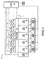
- FIG. 1 Shown in FIG. 1 is a memory 10 having an array 11 of memory cells divided into I/O blocks 14, 16, 18, 20, and 22, a control circuit 12, a row decoder 24, a column decoder 26, a plurality of sense amplifiers (SAs in FIG. 1 ) 28, 32, 36, 40, and 44, a plurality of data buffers (DBs in FIG. 1 ) 30, 34, 38, 42, and 46, and a plurality of source control circuits 48, 50, 52, 54, and 56.
- Each memory cell is a non-volatile memory having a source, a control gate, a drain, and a floating gate.
- a different storage material may be used than a floating gate such as nitride or nanocrystals.
- Row decoder 24 enables a selected word line in I/O blocks 14-22 in response to a row address (not shown).
- Column decoder 26 couples, in response to a column address (not shown), selected bit lines present in I/O blocks 14-22 to respective sense amplifiers and data buffers, 28-46.
- These I/O blocks 14-22 are also coupled to source control circuits 48-56. Only five I/O blocks are shown for convenience, but in an actual memory many more such blocks, e.g., 64, would likely be present. In FIG.
- source control 48, sense amplifier 28, and data buffer 30 correspond to I/O block 14; source control 50, sense amplifier 32, and data buffer 34 correspond to I/O block 16; source control 52, sense amplifier 36, and data buffer 38 correspond to I/O block 18; source control 54, sense amplifier 40, and data buffer 42 correspond to I/O block 20; and source control 56, sense amplifier 44, and data buffer 46 correspond to I/O block 22.
- Control circuit 12 is coupled to source control circuits 48-56, column decoder 26, row decoder 24, and sense amplifiers and data buffers 28-46.
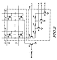
- FIG. 2 Shown in FIG. 2 is a portion of memory 10 of FIG. 1 .
- the portion of I/O block shown in FIG. 1 comprises memory cells 60, 62, 64, and 66; bit lines 74 and 78; and source lines 72 and 76.
- Source control circuit 48 comprises transistors 80, 82, 84, and 86 and resistors 88, 90, and 92.
- the drains of memory cells 60 and 64 are connected to bit line 74.
- the drains of memory cells 62 and 66 are connected to bit line 78.
- the sources of memory cells 60 and 64 are connected to source line 72.
- the sources of memory cells 62 and 66 are connected to source line 76.
- the control gates of memory cells 60 and 62 are connected to word line 68.
- the control gates of memory cells 64 and 66 are connected word line 70.
- source lines 72 and 76 are connected together. All of the sources of the memory cells of memory array 11 are connected together.
- transistor 80 has a drain connected to source lines 72 and 76, a gate connected to a program signal P, and a source.
- Resistor 88 has a first terminal connected to the source of transistor 80 and a second terminal.
- Transistor 82 has drain connected to the second terminal of resistor 88, a source connected to ground, and a gate for receiving a program signal P1.
- Resistor 90 has a first terminal connected the second terminal of resistor 88 and a second terminal.
- Transistor 84 has a drain connected to the second terminal of resistor 90, a source connected to ground, and a gate for receiving a program signal P2.
- Resistor 92 has a first terminal connected to the second terminal of resistor 90 and a second terminal.
- Transistor 86 has a drain connected to the second terminal of resistor 92, a source connected to ground, and a gate for receiving a program signal P3.
- Transistor 58 has a drain connected to source lines 72 and 76, a source connected to ground, and a gate for receiving a READ ENABLE signal.
- Transistor 58 is a representative one of many transistors that are part of array 11 connected to source lines at other locations in memory array 11 for coupling the source lines to ground during a read operation of memory 10.
- the READ ENABLE signal and signals P, P1, P2, and P3 are generated by control circuit 12.
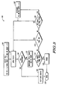
- FIG. 3 Shown in FIG. 3 is a flow chart of a method 100 for operating the memory of FIGs. 1 and 2 to achieve effective programming comprising steps 102, 104, 106, 108, 110, 112, 114, 116, 118, 120, 122.
- the process begins by selecting a cell to be programmed and initializing certain settings.
- One of the settings is initial setting for the total number of programming cycles that have been performed. At the beginning no cycles have been performed so Total Count is set to 0 (zero).
- Total Count is set to 0 (zero).
- the actually programming can be anywhere from no memory cells to 64 memory cells.
- the case of none being programmed occurs when all of the cells were already in the condition that was to be written.
- the condition of all 64 cells being programmed occurs when all of the memory cells were in the erased (one) state and an all zeros condition is to be written.
- a pulse is applied to the drain, via bit line 74, of that cell while its gate, via word line 68, is also at an elevated voltage.
- Typical voltages for the word line and drain in floating gate memories is about 9 volts and 5 volts, respectively. These voltages are likely to decrease as semiconductor technology improvements continue to result in smaller and smaller dimensions for channel lengths and gate dielectrics.
- transistors 84 and 86 are non-conductive.
- Control logic 12 supplies signals P and P1 at a logic high and signals P2 and P3 at a logic low under these initial conditions.
- the READ ENABLE signal 58 is held at a logic low for programming so that transistor 58 is non-conductive during programming. This has the effect of the resistor 88 being in series with the sources of entire array. This resistor is a relatively low resistance, e.g., 250, ohms so that relatively little voltage is dropped across this resistor and thereby not greatly elevating the source voltage. This is effective for fully programming memory cell if the other memory cells connected to bit line 74 do not have too much leakage. If the other cells, such as memory cell 64, do have significant leakage, that will have the effect of reducing the voltage applied to bit line 74 because of the loading of the power supply and of the parasitic resistance that is associated with I/O block 14.
- step 106 is to determine if cell 60 has been in fact programmed.
- Sense amplifier 28 under the control of control circuit 12, detects the state of cell 60 so that control circuit 12 can determine if the programming of cell 60 was sufficient. If it was, then data is flipped in data buffer 30 as shown in step 108, and the programming is done as shown in step 110. If, on the other hand, cell 60 is not considered to be programmed, the total count is incremented and the RS count is incremented as shown in step 112. Then the total count of program cycles, step 114, is compared to the maximum allowed number of program cycles.
- step 114 the first time the criterion of this step 114 is addressed it will not be met, so the answer is no, and the next step would be step 118. If, after additional programming cycles, this criterion of step 114 is met, then that is considered an error and programming cycle is done. If this were to be done at the test level before the product was actually sold, this would be considered a failure and the device would be rejected. Control logic 12 has all the information necessary for making this decision.
- the next step then is increment RS and move to the next RS.
- the source resistance (in this context source resistance is the resistance that is coupled to the commonly-connected sources of the transistors in the memory array) is thus made to be that of resistor 90 plus that of resistor 88.
- Resistor 90 is preferably significantly more resistive than resistor 88, e.g., 2000 ohms. This resistance is designed to provide sufficient resistance to raise the source voltage so that the typical low threshold voltage devices on bit line 74 are made non-conductive during programming.
- the next step is to determine if it was successfully programmed. If so, the data is flipped in data buffer 30 and the programming of this cell 60 is completed.
- the technique utilized resistors which do offer some benefits, to obtain the desired bias on the sources of the array transistors.
- This desired bias could be achieved by another means such as an active biasing circuit.
- the active bias circuit would provide the source bias at a relatively lower voltage for the first programming attempt then a subsequently higher bias to provide needed programming for those that have the excessive leakage on the bit line.
- the technique for altering the source resistance could be altered by having a single resistor matrix for all of array 11 rather than having a separate source control circuit for each I/O block.
- this programming method was discussed in the context of hot carrier injection but could also be used other programming contexts such as in substrate enhanced secondary hot electron injection type programming.
- resistors 88-92 are shown as single resistors but they could, for example, be formed from a plurality of resistors in series.
- the lowest source resistance described was for 250 ohms but this could be different. It could even be essentially zero by simply being the resistance of a switching device and there be no added resistor. Accordingly, the specification and figures are to be regarded in an illustrative rather than a restrictive sense, and all such modifications are intended to be included within the scope of present invention.
Landscapes
- Engineering & Computer Science (AREA)
- Computer Hardware Design (AREA)
- Read Only Memory (AREA)
Applications Claiming Priority (2)
| Application Number | Priority Date | Filing Date | Title |
|---|---|---|---|
| US10/426,282 US6909638B2 (en) | 2003-04-30 | 2003-04-30 | Non-volatile memory having a bias on the source electrode for HCI programming |
| PCT/US2004/011870 WO2004100216A2 (en) | 2003-04-30 | 2004-04-16 | A non-volatile memory having a bias on the source electrode for hci programming |
Publications (3)
| Publication Number | Publication Date |
|---|---|
| EP1623431A2 EP1623431A2 (en) | 2006-02-08 |
| EP1623431A4 EP1623431A4 (en) | 2007-10-17 |
| EP1623431B1 true EP1623431B1 (en) | 2009-10-21 |
Family
ID=33309831
Family Applications (1)
| Application Number | Title | Priority Date | Filing Date |
|---|---|---|---|
| EP04760554A Expired - Lifetime EP1623431B1 (en) | 2003-04-30 | 2004-04-16 | A non-volatile memory having a bias on the source electrode for hci programming |
Country Status (9)
| Country | Link |
|---|---|
| US (1) | US6909638B2 (zh) |
| EP (1) | EP1623431B1 (zh) |
| JP (1) | JP4658039B2 (zh) |
| KR (1) | KR101060034B1 (zh) |
| CN (1) | CN1781157B (zh) |
| AT (1) | ATE446577T1 (zh) |
| DE (1) | DE602004023714D1 (zh) |
| TW (1) | TW200506939A (zh) |
| WO (1) | WO2004100216A2 (zh) |
Families Citing this family (8)
| Publication number | Priority date | Publication date | Assignee | Title |
|---|---|---|---|---|
| US7695843B2 (en) * | 2004-02-13 | 2010-04-13 | Microcell Corporation | Microfibrous fuel cell assemblies comprising fiber-supported electrocatalyst layers, and methods of making same |
| US7227783B2 (en) * | 2005-04-28 | 2007-06-05 | Freescale Semiconductor, Inc. | Memory structure and method of programming |
| US7428172B2 (en) * | 2006-07-17 | 2008-09-23 | Freescale Semiconductor, Inc. | Concurrent programming and program verification of floating gate transistor |
| US7583554B2 (en) | 2007-03-02 | 2009-09-01 | Freescale Semiconductor, Inc. | Integrated circuit fuse array |
| US7787323B2 (en) * | 2007-04-27 | 2010-08-31 | Freescale Semiconductor, Inc. | Level detect circuit |
| KR100965076B1 (ko) * | 2008-11-14 | 2010-06-21 | 주식회사 하이닉스반도체 | 불휘발성 메모리 장치의 프로그램 방법 |
| US7764550B2 (en) * | 2008-11-25 | 2010-07-27 | Freescale Semiconductor, Inc. | Method of programming a non-volatile memory |
| US9312002B2 (en) | 2014-04-04 | 2016-04-12 | Sandisk Technologies Inc. | Methods for programming ReRAM devices |
Family Cites Families (13)
| Publication number | Priority date | Publication date | Assignee | Title |
|---|---|---|---|---|
| JPS57150193A (en) * | 1981-03-13 | 1982-09-16 | Toshiba Corp | Non-volatile semiconductor memory device |
| US4888735A (en) * | 1987-12-30 | 1989-12-19 | Elite Semiconductor & Systems Int'l., Inc. | ROM cell and array configuration |
| US5218571A (en) * | 1990-05-07 | 1993-06-08 | Cypress Semiconductor Corporation | EPROM source bias circuit with compensation for processing characteristics |
| US5923585A (en) * | 1997-01-10 | 1999-07-13 | Invox Technology | Source biasing in non-volatile memory having row-based sectors |
| US5798966A (en) * | 1997-03-31 | 1998-08-25 | Intel Corporation | Flash memory VDS compensation techiques to reduce programming variability |
| JP3920415B2 (ja) * | 1997-03-31 | 2007-05-30 | 三洋電機株式会社 | 不揮発性半導体メモリ装置 |
| US6046932A (en) * | 1999-08-13 | 2000-04-04 | Advanced Micro Devices, Inc. | Circuit implementation to quench bit line leakage current in programming and over-erase correction modes in flash EEPROM |
| US6275415B1 (en) * | 1999-10-12 | 2001-08-14 | Advanced Micro Devices, Inc. | Multiple byte channel hot electron programming using ramped gate and source bias voltage |
| IT1308855B1 (it) * | 1999-10-29 | 2002-01-11 | St Microelectronics Srl | Metodo di riprogrammazione controllata per celle di memoria nonvolatile,in particolare di tipo flash eeprom ed eprom. |
| JP2001195890A (ja) * | 2000-01-12 | 2001-07-19 | Sharp Corp | 不揮発性半導体メモリ装置の書込み方式および書込み回路 |
| JP4559606B2 (ja) * | 2000-09-28 | 2010-10-13 | ルネサスエレクトロニクス株式会社 | 不揮発性半導体記憶装置 |
| JP2003123493A (ja) * | 2001-10-12 | 2003-04-25 | Fujitsu Ltd | ソース電位を制御してプログラム動作を最適化した不揮発性メモリ |
| JP3908957B2 (ja) * | 2002-01-24 | 2007-04-25 | シャープ株式会社 | 不揮発性半導体メモリ装置 |
-
2003
- 2003-04-30 US US10/426,282 patent/US6909638B2/en not_active Expired - Lifetime
-
2004
- 2004-04-16 JP JP2006513084A patent/JP4658039B2/ja not_active Expired - Fee Related
- 2004-04-16 AT AT04760554T patent/ATE446577T1/de not_active IP Right Cessation
- 2004-04-16 DE DE602004023714T patent/DE602004023714D1/de not_active Expired - Lifetime
- 2004-04-16 CN CN2004800111282A patent/CN1781157B/zh not_active Expired - Lifetime
- 2004-04-16 WO PCT/US2004/011870 patent/WO2004100216A2/en active Application Filing
- 2004-04-16 KR KR1020057020573A patent/KR101060034B1/ko active IP Right Grant
- 2004-04-16 EP EP04760554A patent/EP1623431B1/en not_active Expired - Lifetime
- 2004-04-30 TW TW093112134A patent/TW200506939A/zh unknown
Also Published As
| Publication number | Publication date |
|---|---|
| CN1781157A (zh) | 2006-05-31 |
| WO2004100216A3 (en) | 2005-01-06 |
| EP1623431A2 (en) | 2006-02-08 |
| KR101060034B1 (ko) | 2011-08-29 |
| EP1623431A4 (en) | 2007-10-17 |
| DE602004023714D1 (de) | 2009-12-03 |
| CN1781157B (zh) | 2012-02-29 |
| JP2006525622A (ja) | 2006-11-09 |
| WO2004100216B1 (en) | 2005-03-10 |
| WO2004100216A2 (en) | 2004-11-18 |
| US6909638B2 (en) | 2005-06-21 |
| US20040218421A1 (en) | 2004-11-04 |
| JP4658039B2 (ja) | 2011-03-23 |
| TW200506939A (en) | 2005-02-16 |
| KR20060008942A (ko) | 2006-01-27 |
| ATE446577T1 (de) | 2009-11-15 |
Similar Documents
| Publication | Publication Date | Title |
|---|---|---|
| US6888773B2 (en) | Semiconductor memory device and erase method for memory array | |
| US7227783B2 (en) | Memory structure and method of programming | |
| US7952937B2 (en) | Wordline driver for a non-volatile memory device, a non-volatile memory device and method | |
| US7800953B2 (en) | Method and system for selectively limiting peak power consumption during programming or erase of non-volatile memory devices | |
| US6496417B1 (en) | Method and integrated circuit for bit line soft programming (BLISP) | |
| US5583812A (en) | Flash EEPROM system cell array with more than two storage states per memory cell | |
| US7778080B2 (en) | Flash memory array system including a top gate memory cell | |
| EP1203378B1 (en) | Circuit implementation to quench bit line leakage current in programming and over-erase correction modes in flash eeprom | |
| US5357476A (en) | Apparatus and method for erasing a flash EEPROM | |
| US6055184A (en) | Semiconductor memory device having programmable parallel erase operation | |
| US6909639B2 (en) | Nonvolatile memory having bit line discharge, and method of operation thereof | |
| US20030133329A1 (en) | Nonvolatile semiconductor storage device and method for operating the device | |
| KR20030009280A (ko) | Vt 분포를 축소하는 소프트 프로그래밍을 위한 램프된게이트 기법 | |
| JPH03155667A (ja) | フラッシュ消去epromメモリ用の新規なアーキテクチャー | |
| US6172915B1 (en) | Unified erase method in flash EEPROM | |
| EP0108681A2 (en) | Bit erasable electrically erasable programmable read only memory | |
| EP1623431B1 (en) | A non-volatile memory having a bias on the source electrode for hci programming | |
| KR20030011671A (ko) | 메모리 셀 기록 방법 및 회로 | |
| US5995423A (en) | Method and apparatus for limiting bitline current | |
| US7599228B1 (en) | Flash memory device having increased over-erase correction efficiency and robustness against device variations | |
| EP1185985B1 (en) | Method and integrated circuit for bit line soft programming (blisp) | |
| US6349061B1 (en) | Non-volatile semiconductor memory | |
| US5182726A (en) | Circuit and method for discharging a memory array | |
| JPH05182483A (ja) | 不揮発性半導体記憶装置 | |
| KR100378324B1 (ko) | 전기적 프로그램가능 메모리를 구비하는 집적 회로 및고전압 메모리 동작 수행 방법 |
Legal Events
| Date | Code | Title | Description |
|---|---|---|---|
| PUAI | Public reference made under article 153(3) epc to a published international application that has entered the european phase |
Free format text: ORIGINAL CODE: 0009012 |
|
| 17P | Request for examination filed |
Effective date: 20051130 |
|
| AK | Designated contracting states |
Kind code of ref document: A2 Designated state(s): AT BE BG CH CY CZ DE DK EE ES FI FR GB GR HU IE IT LI LU MC NL PL PT RO SE SI SK TR |
|
| R17P | Request for examination filed (corrected) |
Effective date: 20051130 |
|
| RBV | Designated contracting states (corrected) |
Designated state(s): AT BE BG CH CY CZ DE DK EE ES FI FR GB GR HU IE IT LI LU MC NL PL PT RO SE SI SK TR |
|
| DAX | Request for extension of the european patent (deleted) | ||
| A4 | Supplementary search report drawn up and despatched |
Effective date: 20070914 |
|
| RIC1 | Information provided on ipc code assigned before grant |
Ipc: G11C 16/10 20060101AFI20070910BHEP Ipc: G11C 16/34 20060101ALI20070910BHEP Ipc: G11C 16/12 20060101ALI20070910BHEP |
|
| 17Q | First examination report despatched |
Effective date: 20071121 |
|
| GRAP | Despatch of communication of intention to grant a patent |
Free format text: ORIGINAL CODE: EPIDOSNIGR1 |
|
| GRAS | Grant fee paid |
Free format text: ORIGINAL CODE: EPIDOSNIGR3 |
|
| GRAA | (expected) grant |
Free format text: ORIGINAL CODE: 0009210 |
|
| AK | Designated contracting states |
Kind code of ref document: B1 Designated state(s): AT BE BG CH CY CZ DE DK EE ES FI FR GB GR HU IE IT LI LU MC NL PL PT RO SE SI SK TR |
|
| REG | Reference to a national code |
Ref country code: GB Ref legal event code: FG4D |
|
| REG | Reference to a national code |
Ref country code: CH Ref legal event code: EP |
|
| REG | Reference to a national code |
Ref country code: IE Ref legal event code: FG4D |
|
| REF | Corresponds to: |
Ref document number: 602004023714 Country of ref document: DE Date of ref document: 20091203 Kind code of ref document: P |
|
| NLV1 | Nl: lapsed or annulled due to failure to fulfill the requirements of art. 29p and 29m of the patents act | ||
| PG25 | Lapsed in a contracting state [announced via postgrant information from national office to epo] |
Ref country code: ES Free format text: LAPSE BECAUSE OF FAILURE TO SUBMIT A TRANSLATION OF THE DESCRIPTION OR TO PAY THE FEE WITHIN THE PRESCRIBED TIME-LIMIT Effective date: 20100201 Ref country code: SE Free format text: LAPSE BECAUSE OF FAILURE TO SUBMIT A TRANSLATION OF THE DESCRIPTION OR TO PAY THE FEE WITHIN THE PRESCRIBED TIME-LIMIT Effective date: 20091021 Ref country code: PT Free format text: LAPSE BECAUSE OF FAILURE TO SUBMIT A TRANSLATION OF THE DESCRIPTION OR TO PAY THE FEE WITHIN THE PRESCRIBED TIME-LIMIT Effective date: 20100222 Ref country code: FI Free format text: LAPSE BECAUSE OF FAILURE TO SUBMIT A TRANSLATION OF THE DESCRIPTION OR TO PAY THE FEE WITHIN THE PRESCRIBED TIME-LIMIT Effective date: 20091021 |
|
| PG25 | Lapsed in a contracting state [announced via postgrant information from national office to epo] |
Ref country code: SI Free format text: LAPSE BECAUSE OF FAILURE TO SUBMIT A TRANSLATION OF THE DESCRIPTION OR TO PAY THE FEE WITHIN THE PRESCRIBED TIME-LIMIT Effective date: 20091021 Ref country code: PL Free format text: LAPSE BECAUSE OF FAILURE TO SUBMIT A TRANSLATION OF THE DESCRIPTION OR TO PAY THE FEE WITHIN THE PRESCRIBED TIME-LIMIT Effective date: 20091021 |
|
| PG25 | Lapsed in a contracting state [announced via postgrant information from national office to epo] |
Ref country code: BE Free format text: LAPSE BECAUSE OF FAILURE TO SUBMIT A TRANSLATION OF THE DESCRIPTION OR TO PAY THE FEE WITHIN THE PRESCRIBED TIME-LIMIT Effective date: 20091021 Ref country code: AT Free format text: LAPSE BECAUSE OF FAILURE TO SUBMIT A TRANSLATION OF THE DESCRIPTION OR TO PAY THE FEE WITHIN THE PRESCRIBED TIME-LIMIT Effective date: 20091021 |
|
| PG25 | Lapsed in a contracting state [announced via postgrant information from national office to epo] |
Ref country code: BG Free format text: LAPSE BECAUSE OF FAILURE TO SUBMIT A TRANSLATION OF THE DESCRIPTION OR TO PAY THE FEE WITHIN THE PRESCRIBED TIME-LIMIT Effective date: 20100121 Ref country code: EE Free format text: LAPSE BECAUSE OF FAILURE TO SUBMIT A TRANSLATION OF THE DESCRIPTION OR TO PAY THE FEE WITHIN THE PRESCRIBED TIME-LIMIT Effective date: 20091021 Ref country code: DK Free format text: LAPSE BECAUSE OF FAILURE TO SUBMIT A TRANSLATION OF THE DESCRIPTION OR TO PAY THE FEE WITHIN THE PRESCRIBED TIME-LIMIT Effective date: 20091021 Ref country code: RO Free format text: LAPSE BECAUSE OF FAILURE TO SUBMIT A TRANSLATION OF THE DESCRIPTION OR TO PAY THE FEE WITHIN THE PRESCRIBED TIME-LIMIT Effective date: 20091021 |
|
| PLBE | No opposition filed within time limit |
Free format text: ORIGINAL CODE: 0009261 |
|
| STAA | Information on the status of an ep patent application or granted ep patent |
Free format text: STATUS: NO OPPOSITION FILED WITHIN TIME LIMIT |
|
| PG25 | Lapsed in a contracting state [announced via postgrant information from national office to epo] |
Ref country code: CZ Free format text: LAPSE BECAUSE OF FAILURE TO SUBMIT A TRANSLATION OF THE DESCRIPTION OR TO PAY THE FEE WITHIN THE PRESCRIBED TIME-LIMIT Effective date: 20091021 Ref country code: SK Free format text: LAPSE BECAUSE OF FAILURE TO SUBMIT A TRANSLATION OF THE DESCRIPTION OR TO PAY THE FEE WITHIN THE PRESCRIBED TIME-LIMIT Effective date: 20091021 |
|
| 26N | No opposition filed |
Effective date: 20100722 |
|
| PG25 | Lapsed in a contracting state [announced via postgrant information from national office to epo] |
Ref country code: GR Free format text: LAPSE BECAUSE OF FAILURE TO SUBMIT A TRANSLATION OF THE DESCRIPTION OR TO PAY THE FEE WITHIN THE PRESCRIBED TIME-LIMIT Effective date: 20100122 |
|
| PG25 | Lapsed in a contracting state [announced via postgrant information from national office to epo] |
Ref country code: MC Free format text: LAPSE BECAUSE OF NON-PAYMENT OF DUE FEES Effective date: 20100430 |
|
| REG | Reference to a national code |
Ref country code: CH Ref legal event code: PL |
|
| PG25 | Lapsed in a contracting state [announced via postgrant information from national office to epo] |
Ref country code: IE Free format text: LAPSE BECAUSE OF NON-PAYMENT OF DUE FEES Effective date: 20100416 |
|
| PG25 | Lapsed in a contracting state [announced via postgrant information from national office to epo] |
Ref country code: CH Free format text: LAPSE BECAUSE OF NON-PAYMENT OF DUE FEES Effective date: 20100430 Ref country code: LI Free format text: LAPSE BECAUSE OF NON-PAYMENT OF DUE FEES Effective date: 20100430 |
|
| PG25 | Lapsed in a contracting state [announced via postgrant information from national office to epo] |
Ref country code: CY Free format text: LAPSE BECAUSE OF FAILURE TO SUBMIT A TRANSLATION OF THE DESCRIPTION OR TO PAY THE FEE WITHIN THE PRESCRIBED TIME-LIMIT Effective date: 20091021 |
|
| PG25 | Lapsed in a contracting state [announced via postgrant information from national office to epo] |
Ref country code: NL Free format text: LAPSE BECAUSE OF FAILURE TO SUBMIT A TRANSLATION OF THE DESCRIPTION OR TO PAY THE FEE WITHIN THE PRESCRIBED TIME-LIMIT Effective date: 20091021 Ref country code: LU Free format text: LAPSE BECAUSE OF NON-PAYMENT OF DUE FEES Effective date: 20100416 Ref country code: HU Free format text: LAPSE BECAUSE OF FAILURE TO SUBMIT A TRANSLATION OF THE DESCRIPTION OR TO PAY THE FEE WITHIN THE PRESCRIBED TIME-LIMIT Effective date: 20100422 |
|
| PG25 | Lapsed in a contracting state [announced via postgrant information from national office to epo] |
Ref country code: TR Free format text: LAPSE BECAUSE OF FAILURE TO SUBMIT A TRANSLATION OF THE DESCRIPTION OR TO PAY THE FEE WITHIN THE PRESCRIBED TIME-LIMIT Effective date: 20091021 |
|
| PGFP | Annual fee paid to national office [announced via postgrant information from national office to epo] |
Ref country code: GB Payment date: 20140428 Year of fee payment: 11 |
|
| PGFP | Annual fee paid to national office [announced via postgrant information from national office to epo] |
Ref country code: IT Payment date: 20140424 Year of fee payment: 11 Ref country code: FR Payment date: 20140417 Year of fee payment: 11 |
|
| GBPC | Gb: european patent ceased through non-payment of renewal fee |
Effective date: 20150416 |
|
| PG25 | Lapsed in a contracting state [announced via postgrant information from national office to epo] |
Ref country code: GB Free format text: LAPSE BECAUSE OF NON-PAYMENT OF DUE FEES Effective date: 20150416 Ref country code: IT Free format text: LAPSE BECAUSE OF NON-PAYMENT OF DUE FEES Effective date: 20150416 |
|
| REG | Reference to a national code |
Ref country code: FR Ref legal event code: ST Effective date: 20151231 |
|
| PG25 | Lapsed in a contracting state [announced via postgrant information from national office to epo] |
Ref country code: FR Free format text: LAPSE BECAUSE OF NON-PAYMENT OF DUE FEES Effective date: 20150430 |
|
| REG | Reference to a national code |
Ref country code: DE Ref legal event code: R081 Ref document number: 602004023714 Country of ref document: DE Owner name: NXP USA, INC. (N.D.GES.D.STAATES DELAWARE), AU, US Free format text: FORMER OWNER: FREESCALE SEMICONDUCTORS, INC., AUSTIN, TEX., US |
|
| PGFP | Annual fee paid to national office [announced via postgrant information from national office to epo] |
Ref country code: DE Payment date: 20230321 Year of fee payment: 20 |
|
| P01 | Opt-out of the competence of the unified patent court (upc) registered |
Effective date: 20230725 |
|
| REG | Reference to a national code |
Ref country code: DE Ref legal event code: R071 Ref document number: 602004023714 Country of ref document: DE |