EP1619871A2 - Videotakterzeugungsgerät und -Verfahren - Google Patents
Videotakterzeugungsgerät und -Verfahren Download PDFInfo
- Publication number
- EP1619871A2 EP1619871A2 EP05254478A EP05254478A EP1619871A2 EP 1619871 A2 EP1619871 A2 EP 1619871A2 EP 05254478 A EP05254478 A EP 05254478A EP 05254478 A EP05254478 A EP 05254478A EP 1619871 A2 EP1619871 A2 EP 1619871A2
- Authority
- EP
- European Patent Office
- Prior art keywords
- video clock
- clock signals
- predetermined time
- generation
- end video
- Prior art date
- Legal status (The legal status is an assumption and is not a legal conclusion. Google has not performed a legal analysis and makes no representation as to the accuracy of the status listed.)
- Granted
Links
Images


Classifications
-
- H—ELECTRICITY
- H04—ELECTRIC COMMUNICATION TECHNIQUE
- H04N—PICTORIAL COMMUNICATION, e.g. TELEVISION
- H04N1/00—Scanning, transmission or reproduction of documents or the like, e.g. facsimile transmission; Details thereof
- H04N1/04—Scanning arrangements, i.e. arrangements for the displacement of active reading or reproducing elements relative to the original or reproducing medium, or vice versa
- H04N1/047—Detection, control or error compensation of scanning velocity or position
- H04N1/053—Detection, control or error compensation of scanning velocity or position in main scanning direction, e.g. synchronisation of line start or picture elements in a line
-
- G—PHYSICS
- G03—PHOTOGRAPHY; CINEMATOGRAPHY; ANALOGOUS TECHNIQUES USING WAVES OTHER THAN OPTICAL WAVES; ELECTROGRAPHY; HOLOGRAPHY
- G03G—ELECTROGRAPHY; ELECTROPHOTOGRAPHY; MAGNETOGRAPHY
- G03G15/00—Apparatus for electrographic processes using a charge pattern
- G03G15/06—Apparatus for electrographic processes using a charge pattern for developing
- G03G15/08—Apparatus for electrographic processes using a charge pattern for developing using a solid developer, e.g. powder developer
- G03G15/0822—Arrangements for preparing, mixing, supplying or dispensing developer
- G03G15/0848—Arrangements for testing or measuring developer properties or quality, e.g. charge, size, flowability
- G03G15/0856—Detection or control means for the developer level
-
- G—PHYSICS
- G06—COMPUTING OR CALCULATING; COUNTING
- G06F—ELECTRIC DIGITAL DATA PROCESSING
- G06F1/00—Details not covered by groups G06F3/00 - G06F13/00 and G06F21/00
- G06F1/04—Generating or distributing clock signals or signals derived directly therefrom
- G06F1/06—Clock generators producing several clock signals
-
- H—ELECTRICITY
- H04—ELECTRIC COMMUNICATION TECHNIQUE
- H04N—PICTORIAL COMMUNICATION, e.g. TELEVISION
- H04N2201/00—Indexing scheme relating to scanning, transmission or reproduction of documents or the like, and to details thereof
- H04N2201/04—Scanning arrangements
- H04N2201/047—Detection, control or error compensation of scanning velocity or position
- H04N2201/04701—Detection of scanning velocity or position
- H04N2201/04748—Detection of scanning velocity or position by detecting synchronisation signals or driving signals, e.g. page sync
-
- H—ELECTRICITY
- H04—ELECTRIC COMMUNICATION TECHNIQUE
- H04N—PICTORIAL COMMUNICATION, e.g. TELEVISION
- H04N2201/00—Indexing scheme relating to scanning, transmission or reproduction of documents or the like, and to details thereof
- H04N2201/04—Scanning arrangements
- H04N2201/047—Detection, control or error compensation of scanning velocity or position
- H04N2201/04753—Control or error compensation of scanning position or velocity
- H04N2201/04758—Control or error compensation of scanning position or velocity by controlling the position of the scanned image area
- H04N2201/04767—Control or error compensation of scanning position or velocity by controlling the position of the scanned image area by controlling the timing of the signals, e.g. by controlling the frequency o phase of the pixel clock
Definitions
- the present invention relates to an image formation apparatus such as a color laser beam printer using a plurality of laser scanning units (LSU). More particularly, but not exclusively, the present invention relates to a video clock generation apparatus and a method of removing or minimising distortions, such as, errors in video clock signals, produced at the time of generating the video clock signals to compensate for color registration and an offset in laser scanning units of an image formation apparatus.
- LSU laser scanning units
- a conventional image formation apparatus such as a color laser beam printer, includes a ring oscillator, a video clock generation apparatus, a control logic unit, and a multiplexer.
- the ring oscillator generates a predetermined oscillation frequency.
- the video clock generation apparatus uses the oscillation frequency generated by the ring oscillator to generate a video clock signal.
- the control logic and the multiplexer are responsible for preventing errors, such as clock errors preceding and following an effective video clock period required to form images during the appropriate video clock signals.
- the video clock generation apparatus may generate an abnormal video clock signal when attempting to stabilize the loopspeed signal to generate video clock signals.
- an abnormal video clock signal is also generated due to the initialization of the video clock signals for rearranging the main scanning direction of the image formation after the effective video clock period.
- control logic and the multiplexer have been used to convert front-end and back-end video clock signals into system clock signals to remove errors produced during a front-end video clock period preceding the effective video clock period and a back-end video clock period following the effective video clock period, so that the video clock signals can be generated without errors.
- FIG. 1 is a timing diagram showing an example of a conventional system clock (SysClk) and video clock signals (VClk1 and VClk2).
- the system clock SysClk is periodically generated, and the first video clock signal VC1k1 is generated by the video clock generation apparatus.
- Clock errors corresponding to an abnormal video clock are produced in the front-end and back-end video clock periods of the first video clock signal VC1k1.
- the control logic generates the second video clock signal VClk2 by converting the first video clock signal VC1k1 during the front-end and back-end video clock periods to match the system clock SysClk.
- the conversion of the front-end and back-end video clock signals into the system clock signals may produce errors. Therefore, there is a problem in that the errors produced by the clock conversion may cause a malfunction in the resolution enhancement technology (RET) for processing images.
- RET resolution enhancement technology
- Embodiments of the present invention aim to provide a video clock signal generation apparatus for preventing or at least minimising clock errors produced by video clock signal generation for image formation in an image formation apparatus.
- Embodiments of the present invention also aim to provide a video clock generation method for preventing or at least minimising clock errors produced by video clock signal generation for image formation in an image formation apparatus.
- a video clock generation apparatus comprising: a ring oscillator for generating an oscillation frequency; a loopspeed detection unit for detecting a loopspeed representing the number of pulses generated at the oscillation frequency when the ring oscillator oscillates for a predetermined unit time; and a video clock generation unit for suppressing generation of front-end video clock signals for a predetermined initial time, and after a first predetermined time following initialization of effective video clock signals, maintaining the clock state of back-end video clock signals for a second predetermined time, wherein the front-end video clock signals precede the effective video clock signals for image formation and the back-end video clock signals follow the effective video clock signals, and wherein the maintained clock state is the clock state prior to the second predetermined time.
- a video clock generation method comprising the steps of: (a) suppressing a clock generation of a front-end video clock signal preceding an effective video clock signal for image formation for a predetermined initial time; (b) after the predetermined initial time, generating the front-end video clock signal and generating the effective video clock signal after the generation of the front-end video clock signal; (c) after a first predetermined time after initializing the effective video clock signal, maintaining a clock state of back-end video clock signal following the effective video clock signal for a second predetermined time, wherein the clock state is the clock state prior to the second predetermined time; and (d) after the second predetermined time, generating the back-end video clock signal.
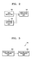
- FIG. 2 is a block diagram of a video clock generation apparatus according to an embodiment of the present invention.
- the video clock generation apparatus comprises a ring oscillator 100, a loopspeed detection unit 120, and a video clock generation unit 140.
- the ring oscillator 100 generates an oscillation frequency. To modulate video clock signals having more than tens of MHz, a frequency higher than that of the video clock signals is required. For this reason, the ring oscillator 100 is used.
- the ring oscillator 100 comprises an odd number of inverter chains. Ideally, one inverter can operate as one tap. In this case, an exact signal between taps cannot be obtained due to a difference between transition times depending on the logic states. In particular, when other devices in the modulator are driven by using tap signals, there occurs a violation of setup/hold time conditions of the memory cells, such as flip-flops. To meet the above conditions, three or five inverters are connected in series to form one converter block that in turn forms one tap.
- the ring oscillator 100 is sensitive to noise so that its oscillation frequency may vary according to a certain operation, temperature, and/or voltage.
- the oscillation frequency generated by the ring oscillator is output to the loopspeed detection unit 120 and the video clock generation unit 140.
- the loopspeed detection unit 120 detects a loopspeed representing the number of pulses oscillated at the oscillation frequency generated by the ring oscillator for a predetermined unit time.
- the predetermined unit time refers to a time period of a system clock generated by the image formation apparatus.
- the loopspeed detection unit 120 detects the loopspeed, that is, the number of pulses oscillated at the oscillation frequency for one period of the system clock, and outputs the detected loopspeed to the video clock generation unit 140.
- the frequency of the video clocks may or may not be about the same frequency as the system clock.
- the effective video clock period corresponds to one horizontal scan line of a laser printer.
- the loopspeed detection unit 120 generates a control signal for suppressing the generation of the front-end video clock signals for a predetermined initial time and outputs the generated control signal to the video clock generation unit 140.
- the front-end video clock signals refer to video clock signals preceding the effective video clock signals for image formation.
- the control signal is a signal for suppressing the generation of the video clock signals until the loopspeed is stabilized.
- the predetermined initial time refers to a time when the ring oscillator 100 and the loopspeed are stabilized.
- the predetermined initial time is approximately set to “8” clock signal cycles, and more preferably, to "16" clock signal cycles after the generation of the oscillation frequency by the ring oscillator 100. Therefore, the control signal can preferably be used to suppress generation of the front-end video clock signals during the "8" or "16" clock signal cycles corresponding to the front-end predetermined initial time.
- the video clock generation unit 140 suppresses the generation of the front-end video clock signals preceding the effective video clock signals for image formation for a predetermined initial time. After a first predetermined time after initializing the clock states of the effective video clock signals, the video clock generation unit 140 maintains the clock state of the back-end video clock signals for a second predetermined time.
- the clock state refers to the clock state prior to the second predetermined time.
- FIG. 3 is a block diagram of a video clock generation unit 140 according to an embodiment of the present invention, which comprises a front-end clock processing unit 200 and a back-end clock processing unit 220.
- the front-end clock processing unit 200 suppresses generation of the front-end video clock signals for the predetermined initial time, depending on the control signal received from the loopspeed detection unit 120, and generates the front-end video clock signals after the predetermined initial time.
- the front-end video clock processing unit 200 suppresses the generation of the front-end video clock signals for the predetermined initial time after frequency oscillation of the ring oscillator 100.
- the clock generation is suppressed for the predetermined initial time is to remove clock errors possibly produced from the front-end video clock signals. Therefore, the clock errors potentially produced from the front-end video clock signals are prevented in advance, so that the quality of image formation can be maintained.
- the front-end video clock processing unit 200 After the predetermined initial time, the front-end video clock processing unit 200 generates the front-end video clock signals depending on the oscillation frequency received from the ring oscillator 100 and the loopspeed detected by the loopspeed detection unit 120. The front-end video clock processing unit 200 outputs the front-end video clock signals generated to the back-end video clock processing unit 220.
- FIG. 4 is a timing diagram showing an example of video clock signals generated according to an embodiment of the present invention. It can be understood that the generation of the front-end video clock signals is suppressed for the predetermined initial time during the front-end video clock period, and the front-end video clock signals are generated, after the predetermined initial time.
- the back-end clock processing unit 220 generates the back-end video clock signals for the first predetermined time after initialization of the effective video clock signals, and maintains the clock state of the back-end video clock for the second predetermined time where the clock state is one prior to the second predetermined time, and generates the back-end video clock signals again after the second predetermined time.
- the back-end video clock processing unit 220 After the initialization of the effective video clock signals for rearranging a main scanning direction of the image formation, the back-end video clock processing unit 220 generates the back-end video clock signals for the first predetermined time depending on the oscillation frequency received from the ring oscillator 100 and the loopspeed detected by the loopspeed detection unit 120. Next, the back-end video clock processing unit 220 maintains the clock state of the back-end video clock for the second predetermined time where the clock state is one prior to the second predetermined time.
- embodiments of the present invention block the errors in advance by maintaining the former video clock state for the video clock signals when the errors are produced. Accordingly, in order to maintain the clock state at the end of first predetermined time, the back-end video clock processing unit 220 processes the back-end video clock signals for the second predetermined time. For example, the clock state maintains low levels at the end of the first predetermined time and the beginning of the second predetermined time, so that the clock signals of the back-end video clock maintain a low level for the second predetermined time, as shown in FIG. 4.
- the back-end video clock processing unit 220 After the second predetermined time, the back-end video clock processing unit 220 generates the back-end video clock signals again, depending on the oscillation frequency received from the ring oscillator 100 and the loopspeed detected by the loopspeed detection unit 120.
- FIG. 5 is a flowchart of a video clock generation method according to an embodiment of the present invention.
- the method comprises the steps of suppressing generation of the front-end video clock signals for a predetermined initial time; and maintaining the clock states of the back-end video clock signals for a second predetermined time where the clock states are the clock states prior to the second predetermined time (operations S300 to S306).
- the predetermined initial time refers to a time to which the ring oscillator 100 and the loopspeed are stabilized.
- the front-end video clock signals are generated after the predetermined initial time, and after the generation of the front-end video clock signals, the effective video clock signals are generated (operation S302).
- the front-end video clock signals are generated, depending on the oscillation frequency received from the ring oscillator 100 and the loopspeed detected by the loopspeed detection unit 120, and after the generation of the front-end video clock signals, the effective video clock signals for image formation are generated.
- the back-end video clock signals following the effective video clock signals maintain the former clock states of the back-end video clock signals for the second predetermined time next to the first predetermined time (operation S304).
- clock errors may be produced after a certain time. Typically, errors are produced after the certain time following the initialization of the effective video clock signals. Therefore, when the effective video clock signals are initialized to rearrange the main scanning direction of the image formation, the back-end video clock signals are generated for the first predetermined time, and then, the back-end video clock signals maintain the former clock state of the back-end video clock signals for the second predetermined time. In other words, the clock errors are prevented by having the clock state of the back-end video clock maintain the video clock state at the end of the first predetermined time, for the second predetermined time corresponding to the moment the glitches are produced.
- the back-end video clock signals are generated after the second predetermined time (operation S306). After the second predetermined time, the back-end video clock signals are generated again, depending on the oscillation frequency received from the ring oscillator 100 and the loopspeed detected by the loopspeed detection unit 120.
- a video clock generation apparatus and method for preventing clock errors, such as errors of the video clock signals, produced by generating video clock signals for image formation in image formation apparatuses, such as laser beam printers, are disclosed. Therefore, it is possible to provide images with good quality.
Landscapes
- Engineering & Computer Science (AREA)
- Multimedia (AREA)
- Signal Processing (AREA)
- Physics & Mathematics (AREA)
- General Physics & Mathematics (AREA)
- Theoretical Computer Science (AREA)
- General Engineering & Computer Science (AREA)
- Synchronizing For Television (AREA)
- Facsimile Scanning Arrangements (AREA)
- Facsimiles In General (AREA)
- Laser Beam Printer (AREA)
- Manipulation Of Pulses (AREA)
Applications Claiming Priority (1)
| Application Number | Priority Date | Filing Date | Title |
|---|---|---|---|
| KR1020040056419A KR100561439B1 (ko) | 2004-07-20 | 2004-07-20 | 비디오 클럭 생성장치 및 방법 |
Publications (3)
| Publication Number | Publication Date |
|---|---|
| EP1619871A2 true EP1619871A2 (de) | 2006-01-25 |
| EP1619871A3 EP1619871A3 (de) | 2007-05-02 |
| EP1619871B1 EP1619871B1 (de) | 2010-09-22 |
Family
ID=35134472
Family Applications (1)
| Application Number | Title | Priority Date | Filing Date |
|---|---|---|---|
| EP05254478A Expired - Lifetime EP1619871B1 (de) | 2004-07-20 | 2005-07-19 | Videotakterzeugungsgerät und -Verfahren |
Country Status (5)
| Country | Link |
|---|---|
| US (1) | US7443534B2 (de) |
| EP (1) | EP1619871B1 (de) |
| KR (1) | KR100561439B1 (de) |
| CN (1) | CN100476573C (de) |
| DE (1) | DE602005023692D1 (de) |
Families Citing this family (2)
| Publication number | Priority date | Publication date | Assignee | Title |
|---|---|---|---|---|
| KR101324186B1 (ko) * | 2007-01-23 | 2013-11-06 | 삼성전자주식회사 | 화상형성장치 및 그 신호 동기화방법 |
| US8115871B2 (en) * | 2008-04-14 | 2012-02-14 | National Semiconductor Corporation | Video top-of-frame signal generator for multiple video formats |
Citations (1)
| Publication number | Priority date | Publication date | Assignee | Title |
|---|---|---|---|---|
| US20030218511A1 (en) | 2002-02-25 | 2003-11-27 | Sony Corporation, A Japanese Corporation | Oscillator and PLL circuit using the same |
Family Cites Families (13)
| Publication number | Priority date | Publication date | Assignee | Title |
|---|---|---|---|---|
| JPS62177569A (ja) * | 1986-01-31 | 1987-08-04 | Toshiba Corp | 記録装置 |
| JP2731151B2 (ja) | 1987-09-18 | 1998-03-25 | 株式会社東芝 | 位相情報検出回路 |
| JP2765582B2 (ja) * | 1988-10-05 | 1998-06-18 | 株式会社リコー | 画像形成装置 |
| US5045811A (en) | 1990-02-02 | 1991-09-03 | Seagate Technology, Inc. | Tuned ring oscillator |
| KR930011511B1 (ko) | 1991-01-28 | 1993-12-08 | 삼성전자 주식회사 | 비디오카메라용 원격제어기 |
| US5471176A (en) | 1994-06-07 | 1995-11-28 | Quantum Corporation | Glitchless frequency-adjustable ring oscillator |
| JP3516154B2 (ja) * | 1995-11-29 | 2004-04-05 | 京セラ株式会社 | レーザビーム走査光学系の走査速度補正方法 |
| JPH1155477A (ja) | 1997-07-31 | 1999-02-26 | Canon Inc | 画像形成装置およびその方法 |
| JP2000043320A (ja) | 1998-07-30 | 2000-02-15 | Mita Ind Co Ltd | 画像形成装置 |
| US6204694B1 (en) | 1999-05-21 | 2001-03-20 | Logicvision, Inc. | Programmable clock signal generation circuits and methods for generating accurate, high frequency, clock signals |
| JP3935308B2 (ja) | 2000-05-17 | 2007-06-20 | 株式会社リコー | 画像処理装置 |
| JP2002100980A (ja) | 2000-09-21 | 2002-04-05 | Ricoh Co Ltd | Dll回路 |
| JP2002331725A (ja) * | 2001-05-08 | 2002-11-19 | Canon Inc | 画像形成装置 |
-
2004
- 2004-07-20 KR KR1020040056419A patent/KR100561439B1/ko not_active Expired - Fee Related
-
2005
- 2005-07-13 US US11/179,465 patent/US7443534B2/en active Active
- 2005-07-19 EP EP05254478A patent/EP1619871B1/de not_active Expired - Lifetime
- 2005-07-19 CN CNB2005100848577A patent/CN100476573C/zh not_active Expired - Fee Related
- 2005-07-19 DE DE602005023692T patent/DE602005023692D1/de not_active Expired - Lifetime
Patent Citations (1)
| Publication number | Priority date | Publication date | Assignee | Title |
|---|---|---|---|---|
| US20030218511A1 (en) | 2002-02-25 | 2003-11-27 | Sony Corporation, A Japanese Corporation | Oscillator and PLL circuit using the same |
Also Published As
| Publication number | Publication date |
|---|---|
| KR100561439B1 (ko) | 2006-03-17 |
| DE602005023692D1 (de) | 2010-11-04 |
| EP1619871B1 (de) | 2010-09-22 |
| EP1619871A3 (de) | 2007-05-02 |
| US20060017984A1 (en) | 2006-01-26 |
| US7443534B2 (en) | 2008-10-28 |
| CN100476573C (zh) | 2009-04-08 |
| CN1725101A (zh) | 2006-01-25 |
| KR20060007584A (ko) | 2006-01-26 |
Similar Documents
| Publication | Publication Date | Title |
|---|---|---|
| JPH11317871A (ja) | パルス幅変調回路 | |
| EP1619871A2 (de) | Videotakterzeugungsgerät und -Verfahren | |
| US6362898B1 (en) | Pulse width position modulator and clock skew synchronizer | |
| US8144350B2 (en) | Image forming apparatus and method of controlling the same | |
| KR100234305B1 (ko) | 화상 형성 장치의 스캐너 비선형성 보정 장치 | |
| JP4361476B2 (ja) | 画像読取装置および画像形成装置 | |
| JP2003039733A (ja) | 光走査装置及び画像形成装置 | |
| JP7508843B2 (ja) | 画像処理装置、画像処理方法、及びプログラム | |
| EP1100258A1 (de) | Vorrichtung zur Periodemessung von Synchronisierungssignal und Anzeigevorrichtung | |
| US20090021545A1 (en) | Image forming apparatus and method of generating output signal thereof | |
| US7369151B2 (en) | Laser control circuit and image forming apparatus | |
| US12567389B2 (en) | Data communication system, and display device | |
| EP1619796A2 (de) | Gerät zur Steuerung eines Ringoszillators und Verfahren welches von Umgebungsänderungen eines Bilderzeugungsgerätes abhängt | |
| US20060103712A1 (en) | Multi-beam image output apparatus and method | |
| JPH1155477A (ja) | 画像形成装置およびその方法 | |
| JP3456425B2 (ja) | 画像形成回路及び画像形成方法 | |
| JP2001326761A (ja) | 画像処理装置 | |
| JP4199025B2 (ja) | 画像形成装置 | |
| JP2009253908A (ja) | 信号処理装置、画像処理装置及び画像形成装置 | |
| JP4391074B2 (ja) | 同期化装置 | |
| JP2000033728A (ja) | デジタルデ―タ同期化方法及び装置 | |
| JP2000043320A (ja) | 画像形成装置 | |
| US20060209339A1 (en) | Apparatus and method for fine tuning a print engine on a line start pixel | |
| JPH04316268A (ja) | 走査ビーム同期制御装置 | |
| JP2006197437A (ja) | 情報処理装置及び画像読取装置 |
Legal Events
| Date | Code | Title | Description |
|---|---|---|---|
| PUAI | Public reference made under article 153(3) epc to a published international application that has entered the european phase |
Free format text: ORIGINAL CODE: 0009012 |
|
| 17P | Request for examination filed |
Effective date: 20050816 |
|
| AK | Designated contracting states |
Kind code of ref document: A2 Designated state(s): AT BE BG CH CY CZ DE DK EE ES FI FR GB GR HU IE IS IT LI LT LU LV MC NL PL PT RO SE SI SK TR |
|
| AX | Request for extension of the european patent |
Extension state: AL BA HR MK YU |
|
| PUAL | Search report despatched |
Free format text: ORIGINAL CODE: 0009013 |
|
| AK | Designated contracting states |
Kind code of ref document: A3 Designated state(s): AT BE BG CH CY CZ DE DK EE ES FI FR GB GR HU IE IS IT LI LT LU LV MC NL PL PT RO SE SI SK TR |
|
| AX | Request for extension of the european patent |
Extension state: AL BA HR MK YU |
|
| 17Q | First examination report despatched |
Effective date: 20070704 |
|
| R17C | First examination report despatched (corrected) |
Effective date: 20070904 |
|
| AKX | Designation fees paid |
Designated state(s): DE FR GB NL |
|
| GRAP | Despatch of communication of intention to grant a patent |
Free format text: ORIGINAL CODE: EPIDOSNIGR1 |
|
| GRAS | Grant fee paid |
Free format text: ORIGINAL CODE: EPIDOSNIGR3 |
|
| GRAA | (expected) grant |
Free format text: ORIGINAL CODE: 0009210 |
|
| AK | Designated contracting states |
Kind code of ref document: B1 Designated state(s): DE FR GB NL |
|
| REG | Reference to a national code |
Ref country code: GB Ref legal event code: FG4D |
|
| REF | Corresponds to: |
Ref document number: 602005023692 Country of ref document: DE Date of ref document: 20101104 Kind code of ref document: P |
|
| REG | Reference to a national code |
Ref country code: NL Ref legal event code: T3 |
|
| PLBE | No opposition filed within time limit |
Free format text: ORIGINAL CODE: 0009261 |
|
| STAA | Information on the status of an ep patent application or granted ep patent |
Free format text: STATUS: NO OPPOSITION FILED WITHIN TIME LIMIT |
|
| 26N | No opposition filed |
Effective date: 20110623 |
|
| REG | Reference to a national code |
Ref country code: DE Ref legal event code: R097 Ref document number: 602005023692 Country of ref document: DE Effective date: 20110623 |
|
| REG | Reference to a national code |
Ref country code: FR Ref legal event code: PLFP Year of fee payment: 12 |
|
| REG | Reference to a national code |
Ref country code: NL Ref legal event code: PD Owner name: S-PRINTING SOLUTION CO., LTD.; KO Free format text: DETAILS ASSIGNMENT: CHANGE OF OWNER(S), ASSIGNMENT; FORMER OWNER NAME: SAMSUNG ELECTRONICS CO., LTD. Effective date: 20170221 |
|
| REG | Reference to a national code |
Ref country code: GB Ref legal event code: 732E Free format text: REGISTERED BETWEEN 20170406 AND 20170412 |
|
| REG | Reference to a national code |
Ref country code: FR Ref legal event code: PLFP Year of fee payment: 13 |
|
| REG | Reference to a national code |
Ref country code: DE Ref legal event code: R081 Ref document number: 602005023692 Country of ref document: DE Owner name: HP PRINTING KOREA CO., LTD., SUWON-SI, KR Free format text: FORMER OWNER: SAMSUNG ELECTRONICS CO., LTD., SUWON-SI, GYEONGGI-DO, KR Ref country code: DE Ref legal event code: R081 Ref document number: 602005023692 Country of ref document: DE Owner name: HEWLETT-PACKARD DEVELOPMENT COMPANY, L.P., SPR, US Free format text: FORMER OWNER: SAMSUNG ELECTRONICS CO., LTD., SUWON-SI, GYEONGGI-DO, KR Ref country code: DE Ref legal event code: R081 Ref document number: 602005023692 Country of ref document: DE Owner name: S-PRINTING SOLUTION CO., LTD., SUWON-SI, KR Free format text: FORMER OWNER: SAMSUNG ELECTRONICS CO., LTD., SUWON-SI, GYEONGGI-DO, KR |
|
| REG | Reference to a national code |
Ref country code: FR Ref legal event code: TP Owner name: S-PRINTING SOLUTION CO., LTD., KR Effective date: 20170912 |
|
| REG | Reference to a national code |
Ref country code: FR Ref legal event code: PLFP Year of fee payment: 14 |
|
| REG | Reference to a national code |
Ref country code: NL Ref legal event code: HC Owner name: HP PRINTING KOREA CO., LTD.; KR Free format text: DETAILS ASSIGNMENT: CHANGE OF OWNER(S), CHANGE OF OWNER(S) NAME; FORMER OWNER NAME: S-PRINTING SOLUTION CO., LTD. Effective date: 20180816 |
|
| REG | Reference to a national code |
Ref country code: DE Ref legal event code: R081 Ref document number: 602005023692 Country of ref document: DE Owner name: HP PRINTING KOREA CO., LTD., SUWON-SI, KR Free format text: FORMER OWNER: S-PRINTING SOLUTION CO., LTD., SUWON-SI, GYEONGGI-DO, KR Ref country code: DE Ref legal event code: R081 Ref document number: 602005023692 Country of ref document: DE Owner name: HEWLETT-PACKARD DEVELOPMENT COMPANY, L.P., SPR, US Free format text: FORMER OWNER: S-PRINTING SOLUTION CO., LTD., SUWON-SI, GYEONGGI-DO, KR |
|
| REG | Reference to a national code |
Ref country code: NL Ref legal event code: PD Owner name: HEWLETT-PACKARD DEVELOPMENT COMPANY, L.P.; US Free format text: DETAILS ASSIGNMENT: CHANGE OF OWNER(S), CHANGE OF LEGAL ENTITY; FORMER OWNER NAME: SAMSUNG ELECTRONICS CO., LTD. Effective date: 20191030 |
|
| REG | Reference to a national code |
Ref country code: DE Ref legal event code: R081 Ref document number: 602005023692 Country of ref document: DE Owner name: HEWLETT-PACKARD DEVELOPMENT COMPANY, L.P., SPR, US Free format text: FORMER OWNER: HP PRINTING KOREA CO., LTD., SUWON-SI, GYEONGGI-DO, KR |
|
| REG | Reference to a national code |
Ref country code: GB Ref legal event code: 732E Free format text: REGISTERED BETWEEN 20191212 AND 20191218 |
|
| PGFP | Annual fee paid to national office [announced via postgrant information from national office to epo] |
Ref country code: FR Payment date: 20200623 Year of fee payment: 16 |
|
| PGFP | Annual fee paid to national office [announced via postgrant information from national office to epo] |
Ref country code: NL Payment date: 20200625 Year of fee payment: 16 Ref country code: GB Payment date: 20200624 Year of fee payment: 16 |
|
| PGFP | Annual fee paid to national office [announced via postgrant information from national office to epo] |
Ref country code: DE Payment date: 20200622 Year of fee payment: 16 |
|
| REG | Reference to a national code |
Ref country code: DE Ref legal event code: R119 Ref document number: 602005023692 Country of ref document: DE |
|
| REG | Reference to a national code |
Ref country code: NL Ref legal event code: MM Effective date: 20210801 |
|
| GBPC | Gb: european patent ceased through non-payment of renewal fee |
Effective date: 20210719 |
|
| PG25 | Lapsed in a contracting state [announced via postgrant information from national office to epo] |
Ref country code: GB Free format text: LAPSE BECAUSE OF NON-PAYMENT OF DUE FEES Effective date: 20210719 Ref country code: DE Free format text: LAPSE BECAUSE OF NON-PAYMENT OF DUE FEES Effective date: 20220201 |
|
| PG25 | Lapsed in a contracting state [announced via postgrant information from national office to epo] |
Ref country code: NL Free format text: LAPSE BECAUSE OF NON-PAYMENT OF DUE FEES Effective date: 20210801 Ref country code: FR Free format text: LAPSE BECAUSE OF NON-PAYMENT OF DUE FEES Effective date: 20210731 |