EP1618397B1 - Messschaltungsanordnung mit erhöhter genauigkeit - Google Patents
Messschaltungsanordnung mit erhöhter genauigkeit Download PDFInfo
- Publication number
- EP1618397B1 EP1618397B1 EP04750816A EP04750816A EP1618397B1 EP 1618397 B1 EP1618397 B1 EP 1618397B1 EP 04750816 A EP04750816 A EP 04750816A EP 04750816 A EP04750816 A EP 04750816A EP 1618397 B1 EP1618397 B1 EP 1618397B1
- Authority
- EP
- European Patent Office
- Prior art keywords
- input
- amplifier
- recited
- differential
- coupled
- Prior art date
- Legal status (The legal status is an assumption and is not a legal conclusion. Google has not performed a legal analysis and makes no representation as to the accuracy of the status listed.)
- Expired - Lifetime
Links
- 238000005259 measurement Methods 0.000 title claims description 57
- NJPPVKZQTLUDBO-UHFFFAOYSA-N novaluron Chemical compound C1=C(Cl)C(OC(F)(F)C(OC(F)(F)F)F)=CC=C1NC(=O)NC(=O)C1=C(F)C=CC=C1F NJPPVKZQTLUDBO-UHFFFAOYSA-N 0.000 claims description 25
- 238000012360 testing method Methods 0.000 claims description 22
- 238000004519 manufacturing process Methods 0.000 claims description 9
- 230000004044 response Effects 0.000 claims description 5
- 238000000034 method Methods 0.000 claims 6
- 238000010586 diagram Methods 0.000 description 3
- 230000002411 adverse Effects 0.000 description 2
- 239000003990 capacitor Substances 0.000 description 2
- 230000008859 change Effects 0.000 description 2
- 230000002950 deficient Effects 0.000 description 1
- 230000001419 dependent effect Effects 0.000 description 1
- 238000013461 design Methods 0.000 description 1
- 230000000694 effects Effects 0.000 description 1
- 230000006872 improvement Effects 0.000 description 1
- 238000009966 trimming Methods 0.000 description 1
Images
Classifications
-
- G—PHYSICS
- G01—MEASURING; TESTING
- G01R—MEASURING ELECTRIC VARIABLES; MEASURING MAGNETIC VARIABLES
- G01R19/00—Arrangements for measuring currents or voltages or for indicating presence or sign thereof
- G01R19/10—Measuring sum, difference or ratio
-
- G—PHYSICS
- G01—MEASURING; TESTING
- G01R—MEASURING ELECTRIC VARIABLES; MEASURING MAGNETIC VARIABLES
- G01R19/00—Arrangements for measuring currents or voltages or for indicating presence or sign thereof
- G01R19/165—Indicating that current or voltage is either above or below a predetermined value or within or outside a predetermined range of values
- G01R19/16566—Circuits and arrangements for comparing voltage or current with one or several thresholds and for indicating the result not covered by subgroups G01R19/16504, G01R19/16528, G01R19/16533
- G01R19/16576—Circuits and arrangements for comparing voltage or current with one or several thresholds and for indicating the result not covered by subgroups G01R19/16504, G01R19/16528, G01R19/16533 comparing DC or AC voltage with one threshold
-
- G—PHYSICS
- G01—MEASURING; TESTING
- G01R—MEASURING ELECTRIC VARIABLES; MEASURING MAGNETIC VARIABLES
- G01R31/00—Arrangements for testing electric properties; Arrangements for locating electric faults; Arrangements for electrical testing characterised by what is being tested not provided for elsewhere
- G01R31/28—Testing of electronic circuits, e.g. by signal tracer
- G01R31/317—Testing of digital circuits
- G01R31/3181—Functional testing
- G01R31/319—Tester hardware, i.e. output processing circuits
- G01R31/31917—Stimuli generation or application of test patterns to the device under test [DUT]
- G01R31/31924—Voltage or current aspects, e.g. driver, receiver
-
- G—PHYSICS
- G01—MEASURING; TESTING
- G01R—MEASURING ELECTRIC VARIABLES; MEASURING MAGNETIC VARIABLES
- G01R31/00—Arrangements for testing electric properties; Arrangements for locating electric faults; Arrangements for electrical testing characterised by what is being tested not provided for elsewhere
- G01R31/28—Testing of electronic circuits, e.g. by signal tracer
- G01R31/317—Testing of digital circuits
- G01R31/3181—Functional testing
- G01R31/319—Tester hardware, i.e. output processing circuits
- G01R31/3193—Tester hardware, i.e. output processing circuits with comparison between actual response and known fault free response
Definitions
- This invention relates generally to measurement circuits used in automatic test equipment, and, more particularly, to measurement circuits employing accurate pedestal sources.
- a fundamental requirement of automatic test systems is the ability to measure accurately electronic signals from devices under test.
- a variety of circuit topologies have been devised for this purpose.
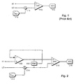
- Fig. 1 shows a high-level example of a measurement circuit that employs an accurate pedestal source 112.
- the pedestal source is generally programmable and is adjusted to produce an accurate voltage V PED approximately equal to an expected differential input voltage HI - LO of the measurement circuit.
- a summing circuit 114 adds a low side (LO) of the measurement circuit to V PED , and a differential amplifier 110 measures the difference between a high side of the measurement circuit (HI) and the output of the summer 114 (LO + V PED ). The output of the differential amplifier is then customarily converted to a digital signal by an analog-to-digital converter 116.
- LO low side
- the measurement circuit can be made to be very precise because V PED can be precisely characterized and can be very stable. We have recognized, however, that the measurement circuit has errors that may adversely affect its performance. For example, offset voltage errors in the differential amplifier 110 induces errors in the measurement circuit. Because the residue is generally a small voltage, it is desirable to operate the differential amplifier 110 at high gain, to assure that the residue is large enough to be readily measured. As is known, however, offset errors of differential amplifiers grow proportionally larger as gain is increased.
- a measurement circuit includes a feedback amplifier and a differential amplifier, each having a first input, a second input, and an output.
- the first input of the feedback amplifier receives an input signal.
- the first input of the differential amplifier is coupled to a pedestal source, and the second input of the differential amplifier is coupled to the output of the feedback amplifier.
- An attenuator is coupled between the first and second inputs of the differential amplifier and provides a feedback signal, which is conveyed to the second input of the feedback circuit.
- the operation of the feedback amplifier effectively boosts the residue signal and therefore allows the differential amplifier to be operated at substantially reduced gain, reducing overall circuit errors.
- Fig. 2 shows an illustrative embodiment of a measurement circuit according to the invention. Certain portions of the measurement circuit of Fig. 2 are similar to those of Fig. 1. For instance, pedestal source 212 is similar to pedestal source 112, summer 214 is similar to summer 114, and ADC 216 is similar to ADC 116. In addition, differential amplifier 210 of Fig. 2 is similar to differential amplifier 110 of Fig. 1, except that it is preferably operated at substantially lower gain.
- the measurement circuit of Fig. 2 also produces a "residue," i.e., a signal indicative of the difference between the input voltage, here HI - LO, and the pedestal voltage, V PED .
- the residue produced in Fig. 2 is substantially larger than the residue produced in Fig. 1.
- the differential amplifier 110 handles the entire task of amplifying the residue to provide a large enough signal that can readily be measured by the ADC 116.
- the differential amplifier 110 and a feedback circuit share this task.
- the feedback circuit provides most or all of the gain for amplifying the residue, and the differential amplifier provides relatively little gain.
- the feedback circuit includes a feedback amplifier 220 and an attenuator 222.
- the attenuator 222 provides a feedback signal to the feedback amplifier 220.
- the attenuator 222 has a nominal attenuation of 1/G, which means that the voltage fed back to the feedback amplifier 220 is V ⁇ + ( V + ⁇ V ⁇ ) / G , where V + and V_ are the non-inverting and inverting inputs of the differential amplifier 210, respectively.
- the HI side of the input voltage is applied to an input of the feedback amplifier 220.
- the LO side of the input voltage is added to the pedestal voltage and applied to the inverting input of the differential amplifier 210.
- the non-inverting (+) input of the differential amplifier 210 is forced to a level that equals HI + ( HI ⁇ ( LO + V PED ) ) ⁇ ( G ⁇ 1 ) .
- This value is exactly the desired quantity, and it is accomplished with the differential amplifier 210 having a gain of only one. After measuring this value, one can compute the actual input voltage, HI - LO, as V PED + V DIFF /G.
- the errors in the circuit of Fig. 2 are much lower than those in the circuit of Fig. 1. Because the output of the differential amplifier V DIFF is divided by G to compute the input voltage, the effect of the differential amplifier's offset voltage on overall circuit performance is negligible.
- the feedback amplifier 220 adds some offset error, but it can be made negligible by selecting a low offset operational amplifier for the feedback amplifier or by trimming the offset of the feedback amplifier to near zero.
- the measurement circuit of Fig. 2 thus effectively transfers the source of offset error from the differential amplifier 210 to the feedback amplifier 220. This may not appear at first to be a substantial improvement. However, many low offset op amps are commercially available, whereas most differential amplifiers have relatively large offset error. Thus, the measurement circuit of Fig. 2 allows better accuracy to be achieved with readily available, commercial components.
- CMRR common mode rejection ratio
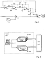
- Fig. 3 shows a more detailed embodiment of the measurement circuit of Fig. 2.
- the feedback amplifier is seen to include three different stages: an input stage 322, and inverter stage 324, and an integrator stage 326.
- Each of these three stages is preferably implemented with a separate operational amplifier (op amp).
- the op amp used for the input stage 322 preferably has a low offset voltage and a high inherent common mode rejection ratio.
- the op amp used for the integrator stage 326 has an input resistor 344, an input capacitor 346, and a feedback capacitor 348, which together dominantly contribute to the open loop gain and frequency response of the feedback amplifier.
- the inverter stage 324 has input and feedback resistors 340 and 342 for achieving the desired inversion for establishing the proper feedback polarity and providing additional open loop gain.
- the inverter stage can be omitted, provided that the inputs to the input stage 322 are reversed to maintain the proper sense of the feedback.
- the attenuator of Fig. 3 is preferably implemented with a pair of resistors 328 and 330.
- the ratio of these resistors sets the gain of the feedback amplifier ("G" from the above equations), where the ratio of resistor 328 to resistor 330 equals G - 1.
- the integrator stage 326 improves the accuracy of the measurement circuit. As is known, integrators have extremely high gain at DC. Therefore, the output of the input stage 322 need only move by minute amounts to establish any desired output voltage of the feedback amplifier as a whole. This is important because the input stage 322 has finite open loop gain, i.e., it can only change its output voltage by experiencing a change in voltage between its non-inverting and inverting inputs. During closed loop operation, changes in output voltage thus effectively cause the circuit to suffer from an output-dependent offset error, which is reflected in the measurement result. The integrator stage 326 virtually eliminates this error by ensuring that the output of the input stage 322 never move by more than minute amounts.
- Fig. 4 shows a typical test environment in which the measurement circuit of Figs. 2 and 3 may be used.
- This test environment includes an automatic test system 400 having a test computer 410 for running a test program (not shown).
- the test computer controls instrumentation, such as stimulus circuits 414 and measurement circuits 416, for exercising a device under test, or "DUT" 412.
- the measurement circuits include the measurement circuit disclosed herein and shown in Figs. 2 and 3.
- the stimulus circuits 414 apply predetermined stimuli to the DUT 412
- the measurement circuits 416 measure voltages and/or currents as responses from the DUT 412.
- the test program compares the measured voltages and/or currents to expected values. If the readings are within allowable tolerances of the expected values, the test program passes. Otherwise, the test program fails.
- the test environment of Fig. 4 is useful in a manufacturing environment, where electronic circuits such as integrated circuits are fabricated. To save manufacturing costs, devices are tested early in the manufacturing process, such as before they are packaged. Devices that pass the test program move on to subsequent manufacturing steps, whereas devices that fail may be discarded. Testing at this level prevents manufacturers from performing expensive fabrication steps on defective devices that are destined to be thrown away, and thus lowers overall manufacturing costs. In addition, the test program may be used to grade devices according to their performance. Devices meeting higher standards may be set aside and sold at higher prices than those performing to lower standards.
- the measurement circuit shown in Figs. 2 and 3 are configured to receive a differential input voltage having both a HI input and a LO input.
- the LO input can be grounded, malcing the input signal effectively single-ended.
- the adder 214/314 can be omitted, and the pedestal source can be coupled directly to the differential amplifier 210/310.
- the HI side of the input signal is more positive than the LO side, but nothing in the design of the measuring circuit requires this.
- the LO side can convey more positive voltages than the HI side, or vice-versa.
- the measurement circuit shown in Figs. 2 and 3 receives an input signal as a voltage (either differential or single-ended), nothing requires that the circuit be used for measuring only voltages from a device under test.
- the measurement circuit can also be used for measuring current, for example, by connecting a shunt resistor between HI and LO and measuring the voltage induced by current flowing across the shunt.
Landscapes
- Physics & Mathematics (AREA)
- General Physics & Mathematics (AREA)
- Engineering & Computer Science (AREA)
- General Engineering & Computer Science (AREA)
- Power Engineering (AREA)
- Amplifiers (AREA)
- Measurement Of Current Or Voltage (AREA)
- Tests Of Electronic Circuits (AREA)
- Testing Electric Properties And Detecting Electric Faults (AREA)
Claims (24)
- Eine Messschaltung, die Folgendes aufweist:einen Differenz- bzw. Differentialverstärker (210) mit einem ersten Eingang und einem zweiten Eingang;eine Basis- bzw. Pedestalspannungsquelle (212), gekoppelt mit dem ersten Eingang des Differenzverstärkers zur Erzeugung eines Basis- bzw. Pedestalsignals, annähernd gleich einer erwarteten Differenzeingangsspannung, gekennzeichnet durcheinen Rückkopplungsverstärker (220) mit einem ersten Eingang zum Empfang eines Eingangssignals (HI), welches gemessen werden soll, einen zweiten Eingang zum Empfang eines Rückkopplungssignals undeinen Ausgang, gekoppelt mit dem zweiten Eingang des Differenzverstärkers (210); undeinen Dämpfer (222), gekoppelt zwischen den ersten und zweiten Eingängen des Differenzverstärkers (210) und zum Liefern des Rückkopplungssignals für den Rückkopplungsverstärker (220).
- Messschaltung nach Anspruch 1, wobei das Eingangssignal am ersten Eingang des Rückkopplungsverstärkers (220) eine HI-Seite eines Differenzeingangssignals ist, wobei die Messschaltung ferner Folgendes aufweist:eine Addierschaltung (214), gekoppelt in Serie mit der Pedestalquelle zum Addieren einer LO-Seite des Differenzeingangssignals zu dem Pedestalsignal.
- Messschaltung nach Anspruch 1, wobei die Dämpfungsvorrichtung bzw. der Dämpfer Folgendes aufweist:eine erste Impedanz (328) mit einem ersten Knoten, gekoppelt mit dem Ausgang des Rückkopplungsverstärkers (220) und mit einem zweiten Knoten, gekoppelt mit dem zweiten Eingang des Rückkopplungsverstärkers (220); undeine zweite Impedanz (330) mit einem ersten Knoten, gekoppelt mit dem zweiten Eingang des Rückkopplungsverstärkers und einem zweiten Eingang, gekoppelt mit dem ersten Eingang des Differenzverstärkers (210).
- Messschaltung nach Anspruch 3, wobei die ersten (328) und die zweiten (330) Impedanzen Widerstände sind, jeweils mit einem Widerstandswert, wobei der Widerstandswert der ersten Impedanz mindestens 100 mal größer ist als der Widerstandswert der zweiten Impedanz.
- Messschaltung nach Anspruch 4, wobei der Differenzverstärker (210) eine Differenzverstärkung von weniger als 100 besitzt.
- Messschaltung nach Anspruch 1, wobei die Pedestalspannungsquelle (212) einen Digital-zu-Analog-Umwandler aufweist.
- Messschaltung nach Anspruch 6, wobei die Pedestalspannungsquelle (212) auf einen Wert programmierbar ist, der gleich einer erwarteten Eingangsspannung der Messschaltung ist.
- Messschaltung nach Anspruch 1, wobei der Rückkopplungsverstärker (220) einen Kompensationsverstärker aufweist zum Vorsehen der gewünschten dynamischen Charakteristika der Rückkopplungsschaltung.
- Messschaltung nach Anspruch 8, wobei der Kompensationsverstärker einen Integrator (326) aufweist.
- Messschaltung nach Anspruch 1, wobei der Rückkopplungsverstärker (220) Folgendes aufweist:eine Eingangsstufe (322) zum Empfang des zu messenden Eingangssignals und des Rückkopplungssignals; undeine Integratorstufe (326) mit einem Eingang, gekoppelt mit dem Ausgang der Eingangsstufe und einem Ausgang, gekoppelt mit dem zweiten Eingang des Differenzverstärkers (310) zum Vorsehen einer hohen Verstärkung bei Gleichspannung.
- Messschaltung nach Anspruch 10, wobei der Rückkopplungsverstärker (220) ferner eine Invertierstufe (324) aufweist, und zwar gekoppelt in Serie zwischen dem Ausgang der Eingangsstufe (322) und dem Eingang der Integratorstufe (326).
- Messschaltung nach Anspruch 11, wobei jede der folgenden Komponenten mindestens einen Operationsverstärker aufweist: die Eingangsstufe (322), die Inverterstufe (324) und die Integratorstufe (326).
- Automatisches Testsystem (400) zum Testen von elektronischen Vorrichtungen, wobei Folgendes vorgesehen ist:ein Computer (410) zum Ausführen eines Testprogramms,eine Vielzahl von Stimulierschaltungen (414) betreibbar unter der Steuerung des Computers; undeine Vielzahl von Messschaltungen (416) nach Anspruch 1 und betreibbar unter der Steuerung des Computers (410).
- Automatisches Testsystem (400) nach Anspruch 13, wobei das Eingangssignal an dem ersten Eingang des Rückkopplungsverstärkers (220) eine HI-Seite eines Differenzeingangssignals ist, und wobei die Messschaltung ferner Folgendes aufweist:eine Addierschaltung (214), gekoppelt in Serie mit der Basis- bzw. Pedestalquelle zum Addieren einer LO-Seite des Differenzeingangssignals zu dem Pedestalsignal.
- Automatisches Testsystem nach Anspruch 13, wobei der Dämpfer Folgendes aufweist:eine erste Impedanz (328) mit einem ersten Knoten, gekoppelt mit dem Ausgang des Rückkopplungsverstärkers (220) und einen zweiten Knoten, gekoppelt mit dem zweiten Eingang des Rückkopplungsverstärkers (220); undeine zweite Impedanz (330) mit einem ersten Knoten, gekoppelt mit dem zweiten Eingang des Rückkopplungsverstärkers und einem zweiten Eingang, gekoppelt mit dem ersten Eingang des Differenzverstärkers.
- Automatisches Testsystem nach Anspruch 15, wobei die ersten (328) und die zweiten (330) Impedanzen Widerstände sind, und zwar jeder mit einem Widerstandswert, wobei der Widerstandswert der ersten Impedanz mindestens 100 mal größer ist als der Widerstandswert der zweiten Impedanz.
- Automatisches Testsystem nach Anspruch 16, wobei der Differenzverstärker (210) eine Differenzverstärkung von weniger als 100 besitzt.
- Verfahren zur Herstellung einer elektronischen Schaltung, wobei Folgendes vorgesehen ist:Ausführen einer Vielzahl von Herstellungsschritten auf der elektronischen Schaltung; undTesten der elektronischen Schaltung zum Überprüfen der Vielzahl von Herstellungsschritten,wobei der Schritt des Testens das Anlegen von Stimuli an die elektronische Schaltung (412) umfasst und das Messen der Ansprechgrößen von der elektronischen Schaltung, und
wobei der Schritt des Messens der Ansprechgrößen eine Messschaltung (416) verwendet, die Folgendes aufweist:einen Differenzverstärker (210) mit einem ersten Eingang und einem zweiten Eingang;eine Pedestalspannungsquelle (212), gekoppelt mit dem ersten Eingang des Differenzverstärkers zur Erzeugung eines Pedestalsignals, annähernd gleich einer erwarteten Differenzeingangsspannung, gekennzeichnet durcheinen Rückkopplungsverstärker (220) mit einem ersten Eingang zum Empfang eines Eingangssignals, einem zweiten Eingang zum Empfang eines Rückkopplungssignals und einem Ausgang, gekoppelt mit dem zweiten Eingang des Differenzverstärkers (210); undeinen Dämpfer (222), gekoppelt zwischen den ersten und zweiten Eingängen des Differenzverstärkers und zum Vorsehen des Rückkopplungssignals für den Rückkopplungsverstärker (220). - Verfahren nach Anspruch 18, wobei der Schritt des Messens von Ansprechgrößen das Lesen von Werten aus der Messschaltung (416) umfasst.
- Verfahren nach Anspruch 19, wobei Folgendes vorgesehen ist:Vergleichen der gelesenen Werte mit Testgrenzen (Testlimits) zur Bestimmung, ob die elektronische Schaltung (412) ihre Tests besteht oder nicht besteht.
- Verfahren nach Anspruch 18, wobei das Eingangssignal am ersten Eingang des Rückkopplungsverstärkers eine HI-Seite eines Differenzeingangssignals ist und wobei die Messschaltung ferner Folgendes aufweist:eine Addierschaltung (214), gekoppelt in Serie mit der Pedestalquelle zum Hinzuaddieren einer LO-Seite des Differenzeingangssignals zu dem Pedestalsignal.
- Verfahren nach Anspruch 18, wobei der Dämpfer Folgendes aufweist:eine erste Impedanz (328) mit einem ersten Knoten, gekoppelt mit dem Ausgang des Rückkopplungsverstärkers und mit einem zweiten Knoten, gekoppelt mit dem zweiten Eingang des Rückkopplungsverstärkers; undeine zweite Impedanz (330) mit einem ersten Knoten, gekoppelt mit dem zweiten Eingang des Rückkopplungsverstärkers und einem zweiten Eingang, gekoppelt mit dem ersten Eingang des Differenzverstärkers.
- Verfahren nach Anspruch 22, wobei die ersten (328) und die zweiten (330) Impedanzen Widerstände sind, jeder mit einem Widerstandswert, wobei der Widerstandswert der ersten Impedanz mindestens 100 mal größer ist als der Widerstandswert der zweiten Impedanz.
- Verfahren nach Anspruch 23, wobei der Differenzverstärker (210) eine Differenzverstärkung von weniger als 100 besitzt.
Applications Claiming Priority (2)
| Application Number | Priority Date | Filing Date | Title |
|---|---|---|---|
| US10/425,329 US6914425B2 (en) | 2003-04-29 | 2003-04-29 | Measurement circuit with improved accuracy |
| PCT/US2004/013109 WO2004097436A2 (en) | 2003-04-29 | 2004-04-27 | Measurement circuit with improved accuracy |
Publications (2)
| Publication Number | Publication Date |
|---|---|
| EP1618397A2 EP1618397A2 (de) | 2006-01-25 |
| EP1618397B1 true EP1618397B1 (de) | 2006-08-30 |
Family
ID=33309676
Family Applications (1)
| Application Number | Title | Priority Date | Filing Date |
|---|---|---|---|
| EP04750816A Expired - Lifetime EP1618397B1 (de) | 2003-04-29 | 2004-04-27 | Messschaltungsanordnung mit erhöhter genauigkeit |
Country Status (9)
| Country | Link |
|---|---|
| US (2) | US6914425B2 (de) |
| EP (1) | EP1618397B1 (de) |
| JP (1) | JP4625453B2 (de) |
| CN (1) | CN100449322C (de) |
| DE (1) | DE602004002209T2 (de) |
| MY (1) | MY136596A (de) |
| SG (1) | SG146469A1 (de) |
| TW (1) | TWI333552B (de) |
| WO (1) | WO2004097436A2 (de) |
Families Citing this family (10)
| Publication number | Priority date | Publication date | Assignee | Title |
|---|---|---|---|---|
| US6914425B2 (en) * | 2003-04-29 | 2005-07-05 | Teradyne, Inc. | Measurement circuit with improved accuracy |
| CN101567729B (zh) * | 2008-04-21 | 2013-07-17 | 北京六合万通微电子技术股份有限公司 | 差分信号强度检测装置 |
| FR2982674B1 (fr) * | 2011-11-10 | 2015-01-16 | Renault Sas | Procede et systeme de mesure de courant electrique |
| US9217780B2 (en) * | 2014-01-07 | 2015-12-22 | Qualcomm Incorporated | Compensation technique for amplifiers in a current sensing circuit for a battery |
| RU2646377C1 (ru) * | 2017-04-11 | 2018-03-02 | Федеральное государственное бюджетное образовательное учреждение высшего образования "Юго-Западный государственный университет "(ЮЗГУ) | Аналоговый интегратор |
| CN110677133B (zh) * | 2019-09-11 | 2023-03-28 | 北京爱尔微科技有限公司 | 一种积分型自适应基线恢复电路 |
| US11156692B2 (en) * | 2020-02-19 | 2021-10-26 | Teradyne, Inc. | Calibrating differential measurement circuitry |
| KR102338892B1 (ko) * | 2020-03-02 | 2021-12-13 | 울산과학기술원 | 생체 신호 처리 장치 |
| KR102424344B1 (ko) * | 2020-09-04 | 2022-07-22 | 울산과학기술원 | 임피던스 부스팅하는 뇌전도 신호 증폭 장치 |
| CN114487615B (zh) * | 2022-04-06 | 2022-08-30 | 基合半导体(宁波)有限公司 | 电容测量电路及电容测量方法 |
Family Cites Families (15)
| Publication number | Priority date | Publication date | Assignee | Title |
|---|---|---|---|---|
| JPS60127572U (ja) * | 1984-02-06 | 1985-08-27 | 株式会社アドバンテスト | 電圧印加電流測定装置 |
| JPS61170137A (ja) * | 1985-01-23 | 1986-07-31 | Nippon Atom Ind Group Co Ltd | アナログ・デイジタル変換装置 |
| GB2263784B (en) * | 1990-01-09 | 1994-02-16 | Richard George Vivian Doble | High frequency measuring circuit |
| JP2542311Y2 (ja) * | 1990-07-13 | 1997-07-23 | 日置電機株式会社 | 電圧検出器 |
| JPH04144423A (ja) * | 1990-10-05 | 1992-05-18 | Jeol Ltd | Adコンバータ |
| NL9200974A (nl) * | 1992-06-03 | 1994-01-03 | Stichting Tech Wetenschapp | Instrumentatieversterker. |
| US5424663A (en) * | 1993-04-22 | 1995-06-13 | North American Philips Corporation | Integrated high voltage differential sensor using the inverse gain of high voltage transistors |
| EP0631144A1 (de) * | 1993-06-24 | 1994-12-28 | Koninklijke Philips Electronics N.V. | Hochspannungdifferentialsensor mit kapazitiver Abschwächung |
| US5514972A (en) * | 1994-10-20 | 1996-05-07 | International Business Machines Corporation | Voltage comparison circuit |
| EP0797794B1 (de) * | 1995-07-21 | 2002-04-03 | Koninklijke Philips Electronics N.V. | Spannungsreferenzanordnung, voltameter, batteriespannung detektionanordnung und ein drahtloses telekommunikationsgerät |
| JP3888592B2 (ja) * | 1996-04-22 | 2007-03-07 | ビービーイー サウンド インク. | 状態変数前置増幅器を有する低入力信号帯域幅圧縮器・増幅器制御回路 |
| US5977824A (en) * | 1996-06-28 | 1999-11-02 | U.S. Philips Corporation | Circuit feedback loop with monitored loop gain |
| JP3186665B2 (ja) * | 1997-09-19 | 2001-07-11 | 三菱電機株式会社 | 位相推定回路および復調回路 |
| JP3863262B2 (ja) * | 1997-09-30 | 2006-12-27 | 松下電器産業株式会社 | 電池電圧測定装置 |
| US6914425B2 (en) * | 2003-04-29 | 2005-07-05 | Teradyne, Inc. | Measurement circuit with improved accuracy |
-
2003
- 2003-04-29 US US10/425,329 patent/US6914425B2/en not_active Expired - Lifetime
-
2004
- 2004-04-26 TW TW093111576A patent/TWI333552B/zh not_active IP Right Cessation
- 2004-04-27 WO PCT/US2004/013109 patent/WO2004097436A2/en not_active Ceased
- 2004-04-27 MY MYPI20041546A patent/MY136596A/en unknown
- 2004-04-27 EP EP04750816A patent/EP1618397B1/de not_active Expired - Lifetime
- 2004-04-27 SG SG200701979-7A patent/SG146469A1/en unknown
- 2004-04-27 DE DE602004002209T patent/DE602004002209T2/de not_active Expired - Fee Related
- 2004-04-27 CN CNB2004800006089A patent/CN100449322C/zh not_active Expired - Lifetime
- 2004-04-27 JP JP2006513400A patent/JP4625453B2/ja not_active Expired - Lifetime
-
2005
- 2005-06-15 US US11/153,104 patent/US7064535B2/en not_active Expired - Lifetime
Also Published As
| Publication number | Publication date |
|---|---|
| MY136596A (en) | 2008-10-31 |
| JP4625453B2 (ja) | 2011-02-02 |
| DE602004002209T2 (de) | 2007-07-26 |
| US20050231189A1 (en) | 2005-10-20 |
| WO2004097436A3 (en) | 2004-12-29 |
| EP1618397A2 (de) | 2006-01-25 |
| TWI333552B (en) | 2010-11-21 |
| US6914425B2 (en) | 2005-07-05 |
| WO2004097436A2 (en) | 2004-11-11 |
| CN100449322C (zh) | 2009-01-07 |
| TW200506400A (en) | 2005-02-16 |
| US20040217809A1 (en) | 2004-11-04 |
| SG146469A1 (en) | 2008-10-30 |
| CN1697979A (zh) | 2005-11-16 |
| JP2006525513A (ja) | 2006-11-09 |
| US7064535B2 (en) | 2006-06-20 |
| DE602004002209D1 (de) | 2006-10-12 |
Similar Documents
| Publication | Publication Date | Title |
|---|---|---|
| JP4255284B2 (ja) | 差動動作のためのシングル・エンド・チャネルの較正 | |
| EP1618397B1 (de) | Messschaltungsanordnung mit erhöhter genauigkeit | |
| US7570114B2 (en) | Common mode rejection calibration method for difference amplifiers | |
| US4841229A (en) | Method of and circuit for ohmmeter calibration | |
| US5424677A (en) | Common mode error correction for differential amplifiers | |
| US6483318B1 (en) | Electric circuit providing selectable short circuit for instrumentation applications | |
| CN113702710B (zh) | 电阻测试电路及电阻测试方法 | |
| US6803776B2 (en) | Current-comparator-based four-terminal resistance bridge for power frequencies | |
| JPH07221613A (ja) | トリガ回路 | |
| US6414496B1 (en) | Comparator structures and methods for automatic test equipment | |
| CN113702711B (zh) | 电阻测试电路及电阻测试方法 | |
| US6825653B2 (en) | Load compensating power supply having minimally invasive device current analyzer | |
| CN117544121A (zh) | 差分放大器和仪表放大器的修调校准方法 | |
| US5020010A (en) | Method for preparing and evaluating measurement specificatons for an electronic circuit | |
| US4733173A (en) | Electronic component measurement apparatus | |
| US4495462A (en) | Current source test circuitry | |
| US6232816B1 (en) | Signal level monitoring circuit | |
| Hess et al. | Evaluation of 100 A, 100 kHz transconductance amplifiers | |
| EP0486114A2 (de) | Elektrischer Testapparat | |
| JPH06100667B2 (ja) | 時間間隔測定装置の校正方法 | |
| Schmitz et al. | On the validity of single-ended mixed-mode s-parameter measurements for differential active devices | |
| Faulkner | HOW THE LOADING OF AN AC/DC TRANSFER STANDARD CAN EFFECT YOUR MEASUREMENTS OF AC VOLTAGE AND CURRENT. | |
| SU784010A1 (ru) | Программируемый формирователь | |
| JP3669516B2 (ja) | 電源供給装置及び電源供給方法 | |
| Gans | Linear Integrated Circuits; Testing and Application |
Legal Events
| Date | Code | Title | Description |
|---|---|---|---|
| PUAI | Public reference made under article 153(3) epc to a published international application that has entered the european phase |
Free format text: ORIGINAL CODE: 0009012 |
|
| 17P | Request for examination filed |
Effective date: 20050105 |
|
| AK | Designated contracting states |
Kind code of ref document: A2 Designated state(s): AT BE BG CH CY CZ DE DK EE ES FI FR GB GR HU IE IT LI LU MC NL PL PT RO SE SI SK TR |
|
| AX | Request for extension of the european patent |
Extension state: AL HR LT LV MK |
|
| GRAP | Despatch of communication of intention to grant a patent |
Free format text: ORIGINAL CODE: EPIDOSNIGR1 |
|
| DAX | Request for extension of the european patent (deleted) | ||
| RBV | Designated contracting states (corrected) |
Designated state(s): DE FR GB IE IT |
|
| GRAS | Grant fee paid |
Free format text: ORIGINAL CODE: EPIDOSNIGR3 |
|
| GRAA | (expected) grant |
Free format text: ORIGINAL CODE: 0009210 |
|
| AK | Designated contracting states |
Kind code of ref document: B1 Designated state(s): DE FR GB IE IT |
|
| PG25 | Lapsed in a contracting state [announced via postgrant information from national office to epo] |
Ref country code: IT Free format text: LAPSE BECAUSE OF FAILURE TO SUBMIT A TRANSLATION OF THE DESCRIPTION OR TO PAY THE FEE WITHIN THE PRESCRIBED TIME-LIMIT;WARNING: LAPSES OF ITALIAN PATENTS WITH EFFECTIVE DATE BEFORE 2007 MAY HAVE OCCURRED AT ANY TIME BEFORE 2007. THE CORRECT EFFECTIVE DATE MAY BE DIFFERENT FROM THE ONE RECORDED. Effective date: 20060830 |
|
| REG | Reference to a national code |
Ref country code: GB Ref legal event code: FG4D |
|
| REG | Reference to a national code |
Ref country code: IE Ref legal event code: FG4D |
|
| REF | Corresponds to: |
Ref document number: 602004002209 Country of ref document: DE Date of ref document: 20061012 Kind code of ref document: P |
|
| ET | Fr: translation filed | ||
| PGFP | Annual fee paid to national office [announced via postgrant information from national office to epo] |
Ref country code: DE Payment date: 20070531 Year of fee payment: 4 |
|
| PLBE | No opposition filed within time limit |
Free format text: ORIGINAL CODE: 0009261 |
|
| STAA | Information on the status of an ep patent application or granted ep patent |
Free format text: STATUS: NO OPPOSITION FILED WITHIN TIME LIMIT |
|
| 26N | No opposition filed |
Effective date: 20070531 |
|
| PGFP | Annual fee paid to national office [announced via postgrant information from national office to epo] |
Ref country code: IE Payment date: 20070924 Year of fee payment: 4 |
|
| PGFP | Annual fee paid to national office [announced via postgrant information from national office to epo] |
Ref country code: FR Payment date: 20070417 Year of fee payment: 4 |
|
| GBPC | Gb: european patent ceased through non-payment of renewal fee |
Effective date: 20080427 |
|
| PG25 | Lapsed in a contracting state [announced via postgrant information from national office to epo] |
Ref country code: DE Free format text: LAPSE BECAUSE OF NON-PAYMENT OF DUE FEES Effective date: 20081101 |
|
| REG | Reference to a national code |
Ref country code: FR Ref legal event code: ST Effective date: 20081231 |
|
| PG25 | Lapsed in a contracting state [announced via postgrant information from national office to epo] |
Ref country code: IE Free format text: LAPSE BECAUSE OF NON-PAYMENT OF DUE FEES Effective date: 20080428 Ref country code: FR Free format text: LAPSE BECAUSE OF NON-PAYMENT OF DUE FEES Effective date: 20080430 |
|
| PG25 | Lapsed in a contracting state [announced via postgrant information from national office to epo] |
Ref country code: GB Free format text: LAPSE BECAUSE OF NON-PAYMENT OF DUE FEES Effective date: 20080427 |