EP1608206B1 - Dispositif d'alimentation de diodes é électroluminescentes avec intensité variable de la lumière - Google Patents
Dispositif d'alimentation de diodes é électroluminescentes avec intensité variable de la lumière Download PDFInfo
- Publication number
- EP1608206B1 EP1608206B1 EP04425437A EP04425437A EP1608206B1 EP 1608206 B1 EP1608206 B1 EP 1608206B1 EP 04425437 A EP04425437 A EP 04425437A EP 04425437 A EP04425437 A EP 04425437A EP 1608206 B1 EP1608206 B1 EP 1608206B1
- Authority
- EP
- European Patent Office
- Prior art keywords
- mode
- control signal
- stage
- light
- driving device
- Prior art date
- Legal status (The legal status is an assumption and is not a legal conclusion. Google has not performed a legal analysis and makes no representation as to the accuracy of the status listed.)
- Expired - Fee Related
Links
Images

Classifications
-
- H—ELECTRICITY
- H05—ELECTRIC TECHNIQUES NOT OTHERWISE PROVIDED FOR
- H05B—ELECTRIC HEATING; ELECTRIC LIGHT SOURCES NOT OTHERWISE PROVIDED FOR; CIRCUIT ARRANGEMENTS FOR ELECTRIC LIGHT SOURCES, IN GENERAL
- H05B45/00—Circuit arrangements for operating light-emitting diodes [LED]
- H05B45/30—Driver circuits
- H05B45/32—Pulse-control circuits
- H05B45/325—Pulse-width modulation [PWM]
-
- H—ELECTRICITY
- H05—ELECTRIC TECHNIQUES NOT OTHERWISE PROVIDED FOR
- H05B—ELECTRIC HEATING; ELECTRIC LIGHT SOURCES NOT OTHERWISE PROVIDED FOR; CIRCUIT ARRANGEMENTS FOR ELECTRIC LIGHT SOURCES, IN GENERAL
- H05B45/00—Circuit arrangements for operating light-emitting diodes [LED]
- H05B45/10—Controlling the intensity of the light
-
- H—ELECTRICITY
- H05—ELECTRIC TECHNIQUES NOT OTHERWISE PROVIDED FOR
- H05B—ELECTRIC HEATING; ELECTRIC LIGHT SOURCES NOT OTHERWISE PROVIDED FOR; CIRCUIT ARRANGEMENTS FOR ELECTRIC LIGHT SOURCES, IN GENERAL
- H05B45/00—Circuit arrangements for operating light-emitting diodes [LED]
- H05B45/30—Driver circuits
- H05B45/37—Converter circuits
- H05B45/3725—Switched mode power supply [SMPS]
- H05B45/385—Switched mode power supply [SMPS] using flyback topology
Definitions
- the present invention relates to a LED driving device with variable light intensity.
- LEDs are increasingly used in the field of lighting, whether industrial or domestic lighting.
- high-efficiency LEDs are commonly used in automotive applications (in particular for the manufacturing the rear lights of motor vehicles), in road signs, or in traffic lights.
- the number of LEDs and the criterion of connection adopted determine the characteristics of the driving device (hereinafter “driver") that must be used for driving the LEDs.
- the value of the output voltage of the driver must increase, while, with the increase in the number of arrays in parallel, the value of the current that the driver must be able to furnish for supplying the LEDs must increase.
- the intensity of current supplied to a LED determines its spectrum of emission and hence the colour of the light emitted. It follows that, to prevent the spectrum of emission of a LED from varying, it is of fundamental importance that the supply current should be kept constant, and hence generally the driver used for driving the LEDs is constituted by a current-controlled DC/DC converter.
- the topology of the DC/DC converter differs according to the type of application envisaged. Normally, the configurations “flyback” or “buck” are used, respectively, if an electrical insulation is required or if the driver is supplied directly by the electric power-supply mains (and hence there is no need to step up the input voltage), whereas the “boost” configuration is used when the driver is battery-supplied and it is hence necessary to step up the input voltage.
- drivers for LEDs comprise a pulse-width-modulation (PWM) control for turning on and turning off LEDs at low-frequency (100-200 Hz), with a ratio between turning-on time and turning-off time (duty cycle) that is a function of the level of light intensity required.
- PWM pulse-width-modulation
- a switch is set in series between the output of the DC/DC converter and the LEDs themselves. Said switch, controlled in PWM, enables or disables the supply of the LEDs. In particular, during the ON phase of the PWM control signal, the switch closes, enabling passage of the supply current to the LEDs and hence their turning-on, while during the OFF phase of the PWM control signal the switch is open, interrupting passage of the supply current and hence causing turning-off of the LEDs.
- the frequency of the PWM control signal is such that the human eye, given the stay time of the image on the retina, does not perceive turning-on and turning-off of the LEDs, since it perceives a light emitted in a constant way.
- US 2003/0085749 A1 discloses a supply assembly for a LED lighting module, comprising a control switch series connected to the LED lighting module; the control switch can be controlled to supply a controlled current to the LED lighting module.
- a dual switching signal composed of low frequency bursts of high frequency pulses is applied to the controlled switch, and by varying the low frequency components of the dual switching signal, the intensity of the light outputted by the LED lighting module can be varied.
- opening of the control switch causes turn-off of the LED module.
- the aim of the present invention is to provide a LED-driving device that is be free from the drawbacks described above, and in particular that enables adjustment of the light intensity of the LEDs in a more economical and efficient way.
- the idea underlying the present invention draws its origin from the consideration that a LED can be considered as a normal diode, with the sole difference that it has a higher threshold voltage V f (normally around 3 V as against the 0.7 V of a normal diode). It follows that a LED automatically turns off when it is biased with a voltage lower than the threshold voltage V f .
- the driving circuit passes from a current control mode to a voltage control mode, which limits the output voltage to a value lower than the threshold voltage of the LEDs.
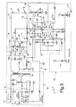
- Figure 1 illustrates a LED-driving device 1.
- the driving device 1 comprises a pair of input terminals 2, 3, receiving a supply voltage V in (in this case, coming from the electric power-supply mains) and a first and a second output terminals 4, 5, connected to the load that must be driven.
- the load is formed by 1 to N arrays 6 of LEDs 7 arranged in parallel, and each array 6 can contain a variable number of LEDs 7 connected in series to each other.
- the driving device 1 moreover comprises an AC/DC converter 8 connected to the input terminals 2, 3 and operating as a rectifier of the mains voltage, and a supply stage 9, cascade-connected to the AC/DC converter 8 and supplying an output voltage V out and an output current I out .
- the supply stage 9 is basically formed by a DC/DC converter and has a first and a second outputs 10a, 10b, connected to the first and the second output terminals 4, 5, respectively.
- a current sensor 11 is connected between the second output terminal 5 of the driving device 1 and the second output 10b of the supply stage 9, and outputs a current-feedback signal V1 fb proportional to the current flowing in the load and co-operating with the supply stage 9 for controlling of the current I out .
- the current sensor 11 comprises a sensing resistor (as described in detail in Figure 3 ).
- the driving device 1 moreover comprises a PWM control circuit 13, of a known type, and an enabling stage 14.
- the PWM control circuit 13 receives an external command, indicated schematically by the arrow 17, and generates a PWM control signal, the pulse width whereof is modifiable via the external control circuit 13, in a known way.
- the enabling stage 14, controlled by the PWM control signal, is connected between the first and second outputs 10a, 10b of the supply stage 9 and outputs a voltage-feedback signal V2 fb having two functions: on the one hand, it enables/disables the voltage control of the supply stage 9; on the other, it supplies an information correlated to the voltage V out .
- the enabling stage 14 comprises a voltage sensor formed by a resistive divider (as illustrated in detail in Figure 3 ), the output signal whereof formes the voltage-feedback signal V2 fb .
- the supply stage 9 can limit the output voltage V out to a value smaller than the threshold voltage of the arrays 6, equal to the sum of the threshold voltages of the LEDs 7 in each array 6. If the arrays 6 contain a different number of LEDs 7, the output voltage V out is limited to a value smaller than the minimum threshold value of the arrays 6. For example, if even just one array 6 is made up of a single LED 7, the output voltage V out is limited to a value smaller than the threshold voltage V f of a LED; for example it can be set at 2 V.
- Operation of the driving device 1 is the following.
- the supply stage 9 works in a current control mode and uses the current-feedback signal V1 fb so that the output current I out has a preset value, such as to forward bias the LEDs 7, which thus conduct and emit light.
- the output current I out has a value equal to the sum of the currents I 1 , ... I N that are to be supplied to the various arrays 6 for forward biasing the LEDs 7.
- the output voltage V out has, instead, a value fixed automatically by the number of driven LEDs 7 (for example, a value of 35 V, when an array 6 is made up of ten LEDs and each LED has an on-voltage drop of 3.5 V).
- the current control enables precise control of the value of the supply current of the LEDs 7 according to the desired spectrum of emission.
- the value of the voltage V out is limited to a value smaller than the minimum threshold voltage of the arrays 6, so causing turning-off of the LEDs 7, as explained in greater detail with reference to Figure 3 .
- the PWM control circuit 13, by varying appropriately the duty cycle of the PWM control signal that controls the enabling stage 14, enables regulation of the intensity of the light emitted by the LEDs 7.
- a duty cycle equal to zero corresponds to a zero light intensity
- a duty cycle equal to one corresponds to a maximum intensity of the light emitted by the LEDs 7.
- Figure 2 shows the time plots of the PWM control signal generated by the PWM control circuit 13, of the output current I out , and of the output voltage V out during normal operation of the driving device 1.
- the supply stage 9 works in a current control mode, outputting the current I out for supply of the LEDs 7; the voltage V out assumes a value, for example 35 V.
- the supply stage 9 works in a voltage control mode, limiting the output voltage V out to a value, for example 2 V, while the current I out goes to zero.
- Figure 3 shows a possible circuit embodiment of the driving device 1, when the driving device 1 is supplied by the electrical power mains and a galvanic insulation is moreover required.
- the current sensor 11 comprises a sensing resistor 20 connected between the second output 10b, which is grounded, of the supply stage 9 and the second output terminal 5.
- the enabling stage 14 comprises a first resistor 27 and a second resistor 28, connected in series.
- the first resistor 27 is connected between the first output terminal 4 and a first intermediate node 31, while the second resistor 28 is connected between the first intermediate node 31 and a second intermediate node 32.
- the voltage-feedback signal V2 fb is present on the first intermediate node 31.
- the enabling stage 14 further comprises a third resistor 37 connected between the second intermediate node 32 and the second output 10b of the supply stage 9, and a bipolar transistor 40 of an NPN type, having its collector terminal connected to the second intermediate node 32, its emitter terminal connected to the second output 10b, and its base terminal receiving the PWM control signal generated in a known way by the PWM control circuit 13.
- the third resistor 37 forms, together with the first resistor 27 and the second resistor 28, a resistive divider 12, controllable via the PWM control signal.
- the supply stage 9 comprises a DC/DC converter 15, of a "flyback" type, cascaded to the AC/DC converter 8 and having the first output 10a and the second output 10b.
- the supply stage 9 moreover comprises a selection stage 16 receiving the current-feedback signal V1 fb and the voltage-feedback signal V2 fb , and having an output connected to a feedback input 26 of the DC/DC converter 15.
- the selection stage 16 alternately feeds the feedback input 26 with the voltage-feedback signal V2 fb and the current-feedback signal V1 fb so as to enable, respectively, voltage control and current control.
- the selection stage 16 comprises a first and a second operational amplifiers 21, 30.
- the first operational amplifier 21 has its inverting terminal connected to the second output terminal 5 and receiving the current-feedback signal V1 fb , its non-inverting terminal receiving a first reference voltage V ref1 , of preset value, and an output connected, via the interposition of a first diode 24, to a feedback node 23, which is in turn connected to the feedback input 26 of the DC/DC converter 15.
- the first diode 24 has its anode connected to the output of the first operational amplifier 21 and its cathode connected to the feedback node 23.
- a first capacitor 25 is connected between the inverting terminal of the first operational amplifier 21 and the cathode of the first diode 24.
- the second operational amplifier 30 has its inverting terminal connected to the first intermediate node 31 and receiving the voltage-feedback signal V2 fb , its non-inverting terminal receiving a second reference voltage V ref2 , of preset value, and an output connected to the feedback node 23 via a second diode 34.
- the second diode 34 has its anode connected to the output of the second operational amplifier 30 and its cathode connected to the feedback node 23.
- a second capacitor 35 is connected between the inverting terminal of the second operational amplifier 30 and the cathode of the second diode 34.
- a first path which comprises the current sensor 11
- a second path which comprises the enabling stage 14, enables, instead, voltage control through the voltage-feedback signal V2 fb , in so far as it detects the value of the output voltage V out via the resistive divider 12.
- the two feedback paths are enabled alternately by the enabling stage 14.
- the transistor 40 acts as a switch controlled by the PWM control signal generated by the PWM control circuit 13, determining, with its opening and its closing, two different division ratios of the resistive divider 12 and hence different values of the voltage-feedback signal V2 fb .
- the third resistor 37 is shortcircuited and the resistive divider 12 is formed only by the first resistor 27 and second resistor 28 having resistances R 1 and R 2 , respectively.
- the inverting terminal of the second operational amplifier 30 is at a potential V2 fb1 smaller than that of the non-inverting terminal receiving the second reference voltage V ref2 , so that the output of the second operational amplifier 30 becomes positive, causing an off-state of the second diode 34.
- the first operational amplifier 21 receives, on its inverting terminal, a voltage V1 fb proportional to the current flowing in the sensing resistor 20, greater than the first reference voltage V ref1 , and hence the first diode 24 is on.
- the first reference voltage V ref1 has a low value (for example, 100 mV) so as to limit the power dissipation on the sensing resistor 20.
- the inverting terminal of the second operational amplifier 30 is at a potential V2 fb2 higher than that of the non-inverting terminal, receiving the second reference voltage V ref2 , so that the output of the second operational amplifier 30 becomes negative, causing turning-on of the second diode 34. Instead, in this situation, the first diode 24 is turned off. In this way, the feedback node 23 is connected to the second feedback path, and consequently the voltage control is enabled, which limits the output voltage V out to a value lower than the threshold voltage of the array 6, as described above.
- the value of the second reference voltage V ref2 supplied to the non-inverting terminal of the second operational amplifier 30, and the values of the resistances are chosen so that the output voltage V out assumes the desired value.
- the driving device described herein presents the following advantages.
Claims (18)
- Dispositif (1) pour commander un élément à diodes électroluminescentes (6), avec une intensité lumineuse variable, ayant une tension de seuil d'activation, comprenant :- un étage d'alimentation (9) comportant une sortie (10a, 10b) destinée à être connectée audit élément à diodes électroluminescentes (6), ledit étage d'alimentation (9) étant configuré de manière à avoir un premier mode de fonctionnement, dans lequel ledit étage d'alimentation (9) génère un courant d'alimentation contrôlé (Iout)- un capteur de courant (11), pouvant être connecté à ladite sortie (10a, 10b) pour générer, en utilisation, un signal de rétroaction de courant (V1fb) corrélé avec le courant circulant dans ledit élément à diodes électroluminescentes (6) et envoyé audit étage d'alimentation (9) dans ledit premier mode de fonctionnement,caractérisé en ce que ledit étage d'alimentation (9) est en outre configuré de manière à avoir un deuxième mode de fonctionnement, dans lequel ledit étage d'alimentation (9) génère une tension d' alimentation contrôlée (Vout) ayant une valeur positive non nulle inférieure à ladite tension de seuil d'activation, de manière à polariser ledit élément à diodes électroluminescentes (6) au-dessous du seuil, provoquant de ce fait sa désactivation ; et en ce qu'il comprend en outre :- un étage de commande d'intensité (13, 14) générant un signal de commande de mode (V2fb) envoyé audit étage d'alimentation (9) et commandant la commutation séquentielle entre lesdits premier et deuxième modes de fonctionnement dudit étage d'alimentation (9) en fonction d'une intensité lumineuse souhaitée.
- Dispositif de commande selon la revendication 1, dans lequel ledit étage de commande d'intensité (13, 14) est configuré pour générer ledit signal de commande de mode (V2fb) envoyé audit étage d'alimentation sur la base d'une tension aux bornes dudit élément à diodes électroluminescentes (6).
- Dispositif de commande selon la revendication 1 ou 2 pour un élément à diodes électroluminescentes (6) comprenant une pluralité de DEL (7) connectées en série et ayant une tension de seuil propre ; dans lequel ladite tension de seuil d'activation est égale à la somme desdites tensions de seuil propres desdites DEL (7).
- Dispositif de commande selon l'une quelconque des revendications précédentes, dans lequel ledit signal de commande de mode (V2fb) est un signal périodique définissant un premier intervalle de temps et un deuxième intervalle de temps correspondant auxdits premier et deuxième modes de fonctionnement, ledit étage de commande d'intensité (13, 14) comprenant des moyens de régulation (13) pour réguler lesdits premier et deuxième intervalles de temps.
- Dispositif de commande selon la revendication 4, dans lequel lesdits moyens de régulation comprennent un modulateur de durée d'impulsion - PWM (13).
- Dispositif de commande selon la revendication 4 ou 5, dans lequel ledit étage de commande d'intensité (13, 14) comprend en outre un étage de validation (14) connecté entre lesdits moyens de régulation (13) et ledit étage d'alimentation (9) et générant ledit signal de commande de mode (V2fb).
- Dispositif de commande selon la revendication 6, dans lequel ledit étage de validation (14) comprend un diviseur résistif (12) couplé à ladite sortie (10a, 10b) dudit étage d'alimentation (9), et comportant un premier noeud intermédiaire (31) délivrant ledit signal de commande de mode (V2fb) et des moyens (40) pour modifier le rapport de division, commandés par lesdits moyens de régulation (13).
- Dispositif de commande selon la revendication 7, dans lequel ledit étage d'alimentation (9) comprend un régulateur (15) et un étage de sélection (16), ledit régulateur (15) comportant une entrée de rétroaction (26) et ledit étage de sélection (16) recevant ledit signal de commande de mode (V2fb) et ledit signal de rétroaction de courant (V1fb) et délivrant à ladite entrée de rétroaction (26) alternativement ledit signal de rétroaction de courant (V1fb) dans ledit premier mode de fonctionnement et ledit signal de commande de mode (V2fb) dans ledit deuxième mode de fonctionnement.
- Dispositif de commande selon la revendication 8, dans lequel ledit étage de sélection (16) comprend un circuit de comparaison (21, 30) recevant ledit signal de rétroaction de courant (V1fb), ledit signal de commande de mode (V2fb) et un signal de référence (Vref2) et appliquant à ladite entrée de rétroaction (26) ledit signal de rétroaction de courant (V1fb) en présence d'une première relation entre ledit signal de commande de mode (V2fb) et ledit signal de référence (Vref2), et ledit signal de commande de mode (V2fb) en présence d'une deuxième relation entre ledit signal de commande de mode (V2fb) et ledit signal de référence (Vref2) .
- Dispositif de commande selon la revendication 9, dans lequel ledit circuit de comparaison (21, 30) comprend des moyens formant amplificateur opérationnel (30) comportant une première borne recevant ledit signal de commande de mode (V2fb), une deuxième borne recevant ladite tension de référence (Vref2), et une sortie connectée à ladite entrée de rétroaction (26) par l'intermédiaire de moyens unidirectionnels (34).
- Dispositif de commande selon la revendication 10, dans lequel lesdits moyens unidirectionnels comprennent une diode (34) dont la cathode est connectée à ladite entrée de rétroaction (26) et dont l'anode est connectée à la sortie desdits moyens formant amplificateur opérationnel (30).
- Dispositif de commande selon l'une quelconque des revendications 7 à 11, dans lequel ledit étage d'alimentation (9) a des première et deuxième sorties (10a, 10b), et ledit diviseur résistif (12) comprend des premiers moyens résistifs (27) connectés entre ladite première sortie (10a) et ledit premier noeud intermédiaire (31), des deuxièmes moyens résistifs (28) connectés entre ledit premier noeud intermédiaire (31) et un deuxième noeud intermédiaire (32), et des troisièmes moyens résistifs (37) connectés entre ledit deuxième noeud intermédiaire (32) et ladite deuxième sortie (10b) ; lesdits moyens de modification de rapport de division comprenant des moyens de commutation (40) connectés en parallèle avec lesdits troisièmes moyens résistifs (37) et commandés par lesdits moyens de régulation (13).
- Dispositif de commande selon la revendication 12, dans lequel lesdits moyens de commutation comprennent des moyens formant transistor (40) dont une première borne de conduction est connectée audit deuxième noeud intermédiaire (32), une deuxième borne de conduction est connectée à ladite deuxième sortie (10b), et une borne de commande est connectée auxdits moyens de régulation (13).
- Procédé pour commander un élément à diodes électroluminescentes (6), ayant une tension de seuil d'activation, avec une intensité lumineuse variable, comprenant l'étape consistant à :- alimenter ledit élément à diodes électroluminescentes (6) avec un courant d'alimentation contrôlé (Iout) dans un premier mode de fonctionnement, ladite étape d'alimentation comprenant la commande dudit courant d'alimentation (Iout) au moyen d'un signal de rétroaction de courant (V1fb) corrélé avec le courant circulant dans ledit élément à diodes électroluminescentes (6) ;caractérisé en ce qu'il comprend en outre les étapes consistant à :- alimenter ledit élément à diodes électroluminescentes (6) avec une tension d' alimentation contrôlée (Vout) dans un deuxième mode de fonctionnement, ladite tension d'alimentation contrôlée (Vout) ayant une valeur non nulle inférieure à ladite tension de seuil d'activation dudit élément à diodes électroluminescentes (6), de manière à polariser ledit élément à diodes électroluminescentes (6) au-dessous du seuil, provoquant de ce fait sa désactivation ; et- commander alternativement une commutation séquentielle entre lesdits premier et deuxième modes de fonctionnement, en fonction d'une intensité lumineuse souhaitée.
- Procédé selon la revendication 14, dans lequel ladite étape consistant à commander alternativement comprend la génération d'un signal de commande de mode (V2fb) sur la base d'une tension aux bornes dudit élément à diodes électroluminescentes (6).
- Procédé selon la revendication 14 ou 15, dans lequel ladite étape consistant à commander alternativement comprend l'étape de génération d'un signal de commande de mode périodique (V2fb), définissant un premier intervalle de temps et un deuxième intervalle de temps correspondant audit premier mode de fonctionnement et audit deuxième mode de fonctionnement, respectivement, le procédé comprenant en outre l'étape consistant à réguler la durée dudit premier intervalle de temps et dudit deuxième intervalle de temps.
- Procédé selon la revendication 16, dans lequel ladite étape consistant à réguler comprend la génération d'un signal de commande modulé par durée d'impulsion (PWM).
- Procédé selon la revendication 16, dans lequel ledit signal de commande de mode (V2fb) est proportionnel à une tension de sortie aux bornes dudit élément à diodes électroluminescentes (6) ; et ladite étape consistant à commander alternativement comprend la modification du rapport de proportionnalité entre ledit signal de commande de mode (V2fb) et ladite tension de sortie, la comparaison dudit signal de commande de mode (V2fb) avec un signal de référence (Vref2), et la validation alternativement desdits premier et deuxième modes de fonctionnement en fonction du résultat de ladite comparaison.
Priority Applications (4)
| Application Number | Priority Date | Filing Date | Title |
|---|---|---|---|
| EP04425437A EP1608206B1 (fr) | 2004-06-14 | 2004-06-14 | Dispositif d'alimentation de diodes é électroluminescentes avec intensité variable de la lumière |
| DE602004022518T DE602004022518D1 (de) | 2004-06-14 | 2004-06-14 | LED-Ssteuergeräte mit Lichtintensitätsänderung |
| US11/153,848 US7750579B2 (en) | 2004-06-14 | 2005-06-14 | LED driving device with variable light intensity |
| US12/773,724 US8125159B2 (en) | 2004-06-14 | 2010-05-04 | LED driving device with variable light intensity |
Applications Claiming Priority (1)
| Application Number | Priority Date | Filing Date | Title |
|---|---|---|---|
| EP04425437A EP1608206B1 (fr) | 2004-06-14 | 2004-06-14 | Dispositif d'alimentation de diodes é électroluminescentes avec intensité variable de la lumière |
Publications (2)
| Publication Number | Publication Date |
|---|---|
| EP1608206A1 EP1608206A1 (fr) | 2005-12-21 |
| EP1608206B1 true EP1608206B1 (fr) | 2009-08-12 |
Family
ID=34932561
Family Applications (1)
| Application Number | Title | Priority Date | Filing Date |
|---|---|---|---|
| EP04425437A Expired - Fee Related EP1608206B1 (fr) | 2004-06-14 | 2004-06-14 | Dispositif d'alimentation de diodes é électroluminescentes avec intensité variable de la lumière |
Country Status (3)
| Country | Link |
|---|---|
| US (2) | US7750579B2 (fr) |
| EP (1) | EP1608206B1 (fr) |
| DE (1) | DE602004022518D1 (fr) |
Cited By (1)
| Publication number | Priority date | Publication date | Assignee | Title |
|---|---|---|---|---|
| CN109498999A (zh) * | 2018-12-07 | 2019-03-22 | 中国电子科技集团公司第四十研究所 | 一种红外偏振光治疗仪光强调节电路 |
Families Citing this family (93)
| Publication number | Priority date | Publication date | Assignee | Title |
|---|---|---|---|---|
| KR100674873B1 (ko) * | 2005-06-15 | 2007-01-30 | 삼성전기주식회사 | 백라이트 인버터의 시간 제어회로 |
| US7286123B2 (en) * | 2005-12-13 | 2007-10-23 | System General Corp. | LED driver circuit having temperature compensation |
| WO2007125466A1 (fr) * | 2006-05-02 | 2007-11-08 | Philips Intellectual Property & Standards Gmbh | Circuit a diodes lumineuses, et montage et dispositif associes |
| CN101480105B (zh) * | 2006-06-26 | 2011-07-20 | 皇家飞利浦电子股份有限公司 | 利用恒定电流来驱动负载的驱动电路 |
| US8035313B2 (en) * | 2006-10-06 | 2011-10-11 | Koninklijke Philips Electronics N.V. | Light element array with controllable current sources and method of operation |
| EP2078446B1 (fr) * | 2006-10-06 | 2013-04-10 | Philips Intellectual Property & Standards GmbH | Matrice d'éléments lumineux commutables et procédé de fonctionnement |
| TWI326563B (en) * | 2006-10-18 | 2010-06-21 | Chunghwa Picture Tubes Ltd | Light source driving circuit |
| US8362838B2 (en) * | 2007-01-19 | 2013-01-29 | Cirrus Logic, Inc. | Multi-stage amplifier with multiple sets of fixed and variable voltage rails |
| US8076920B1 (en) | 2007-03-12 | 2011-12-13 | Cirrus Logic, Inc. | Switching power converter and control system |
| US8018171B1 (en) | 2007-03-12 | 2011-09-13 | Cirrus Logic, Inc. | Multi-function duty cycle modifier |
| US7667408B2 (en) | 2007-03-12 | 2010-02-23 | Cirrus Logic, Inc. | Lighting system with lighting dimmer output mapping |
| US20080224631A1 (en) * | 2007-03-12 | 2008-09-18 | Melanson John L | Color variations in a dimmable lighting device with stable color temperature light sources |
| US7288902B1 (en) * | 2007-03-12 | 2007-10-30 | Cirrus Logic, Inc. | Color variations in a dimmable lighting device with stable color temperature light sources |
| US7852017B1 (en) | 2007-03-12 | 2010-12-14 | Cirrus Logic, Inc. | Ballast for light emitting diode light sources |
| JP2008235199A (ja) * | 2007-03-23 | 2008-10-02 | Harison Toshiba Lighting Corp | 放電灯点灯装置、画像投影装置 |
| GB0706719D0 (en) * | 2007-04-06 | 2007-05-16 | H W D Ltd | Lens selection system |
| US7554473B2 (en) | 2007-05-02 | 2009-06-30 | Cirrus Logic, Inc. | Control system using a nonlinear delta-sigma modulator with nonlinear process modeling |
| US7696913B2 (en) | 2007-05-02 | 2010-04-13 | Cirrus Logic, Inc. | Signal processing system using delta-sigma modulation having an internal stabilizer path with direct output-to-integrator connection |
| EP2158794B1 (fr) * | 2007-06-15 | 2011-12-28 | Tridonic GmbH & Co KG | Appareil permettant de faire fonctionner une source de lumière, notamment une del |
| US8102127B2 (en) * | 2007-06-24 | 2012-01-24 | Cirrus Logic, Inc. | Hybrid gas discharge lamp-LED lighting system |
| US7800315B2 (en) * | 2007-09-21 | 2010-09-21 | Exclara, Inc. | System and method for regulation of solid state lighting |
| KR101614304B1 (ko) | 2007-11-16 | 2016-04-21 | 알레그로 마이크로시스템스, 엘엘씨 | 직렬 연결된 발광 다이오드 열들을 구동하는 전자 회로들 |
| US7804697B2 (en) * | 2007-12-11 | 2010-09-28 | Cirrus Logic, Inc. | History-independent noise-immune modulated transformer-coupled gate control signaling method and apparatus |
| JP5042798B2 (ja) * | 2007-12-17 | 2012-10-03 | 株式会社小糸製作所 | 車両用灯具の点灯制御装置 |
| IL188348A0 (en) | 2007-12-24 | 2008-11-03 | Lightech Electronics Ind Ltd | Controller and method for controlling an intensity of a light emitting diode (led) using a conventional ac dimmer |
| US8576589B2 (en) | 2008-01-30 | 2013-11-05 | Cirrus Logic, Inc. | Switch state controller with a sense current generated operating voltage |
| US8022683B2 (en) | 2008-01-30 | 2011-09-20 | Cirrus Logic, Inc. | Powering a power supply integrated circuit with sense current |
| US7755525B2 (en) * | 2008-01-30 | 2010-07-13 | Cirrus Logic, Inc. | Delta sigma modulator with unavailable output values |
| US8008898B2 (en) * | 2008-01-30 | 2011-08-30 | Cirrus Logic, Inc. | Switching regulator with boosted auxiliary winding supply |
| JP2009184592A (ja) * | 2008-02-08 | 2009-08-20 | Koito Mfg Co Ltd | 車両用灯具の点灯制御装置 |
| JP4687735B2 (ja) * | 2008-03-24 | 2011-05-25 | 東芝ライテック株式会社 | 電源装置及び照明器具 |
| US7759881B1 (en) | 2008-03-31 | 2010-07-20 | Cirrus Logic, Inc. | LED lighting system with a multiple mode current control dimming strategy |
| US8008902B2 (en) * | 2008-06-25 | 2011-08-30 | Cirrus Logic, Inc. | Hysteretic buck converter having dynamic thresholds |
| US8344707B2 (en) | 2008-07-25 | 2013-01-01 | Cirrus Logic, Inc. | Current sensing in a switching power converter |
| US8279628B2 (en) * | 2008-07-25 | 2012-10-02 | Cirrus Logic, Inc. | Audible noise suppression in a resonant switching power converter |
| US8212491B2 (en) | 2008-07-25 | 2012-07-03 | Cirrus Logic, Inc. | Switching power converter control with triac-based leading edge dimmer compatibility |
| US8487546B2 (en) | 2008-08-29 | 2013-07-16 | Cirrus Logic, Inc. | LED lighting system with accurate current control |
| JP4600583B2 (ja) | 2008-09-10 | 2010-12-15 | 東芝ライテック株式会社 | 調光機能を有する電源装置及び照明器具 |
| US8222872B1 (en) | 2008-09-30 | 2012-07-17 | Cirrus Logic, Inc. | Switching power converter with selectable mode auxiliary power supply |
| US8179110B2 (en) * | 2008-09-30 | 2012-05-15 | Cirrus Logic Inc. | Adjustable constant current source with continuous conduction mode (“CCM”) and discontinuous conduction mode (“DCM”) operation |
| DE102008055862A1 (de) * | 2008-11-05 | 2010-05-06 | Tridonicatco Gmbh & Co. Kg | Leuchtmittel-Betriebsgerät mit Potentialtrennung |
| US8288954B2 (en) | 2008-12-07 | 2012-10-16 | Cirrus Logic, Inc. | Primary-side based control of secondary-side current for a transformer |
| US8299722B2 (en) | 2008-12-12 | 2012-10-30 | Cirrus Logic, Inc. | Time division light output sensing and brightness adjustment for different spectra of light emitting diodes |
| US8362707B2 (en) | 2008-12-12 | 2013-01-29 | Cirrus Logic, Inc. | Light emitting diode based lighting system with time division ambient light feedback response |
| US7994863B2 (en) * | 2008-12-31 | 2011-08-09 | Cirrus Logic, Inc. | Electronic system having common mode voltage range enhancement |
| JP4998808B2 (ja) * | 2009-03-02 | 2012-08-15 | ブラザー工業株式会社 | 光出力装置および当該光出力装置を備えた画像形成装置 |
| JP5515931B2 (ja) | 2009-04-24 | 2014-06-11 | 東芝ライテック株式会社 | 発光装置及び照明装置 |
| US8482223B2 (en) | 2009-04-30 | 2013-07-09 | Cirrus Logic, Inc. | Calibration of lamps |
| JP2010267415A (ja) * | 2009-05-12 | 2010-11-25 | Toshiba Lighting & Technology Corp | 照明装置 |
| US8198874B2 (en) * | 2009-06-30 | 2012-06-12 | Cirrus Logic, Inc. | Switching power converter with current sensing transformer auxiliary power supply |
| US8963535B1 (en) | 2009-06-30 | 2015-02-24 | Cirrus Logic, Inc. | Switch controlled current sensing using a hall effect sensor |
| US8248145B2 (en) | 2009-06-30 | 2012-08-21 | Cirrus Logic, Inc. | Cascode configured switching using at least one low breakdown voltage internal, integrated circuit switch to control at least one high breakdown voltage external switch |
| US8212493B2 (en) | 2009-06-30 | 2012-07-03 | Cirrus Logic, Inc. | Low energy transfer mode for auxiliary power supply operation in a cascaded switching power converter |
| US7862173B1 (en) | 2009-07-29 | 2011-01-04 | VistaMed, LLC | Digital imaging ophthalmoscope |
| JP2012023001A (ja) | 2009-08-21 | 2012-02-02 | Toshiba Lighting & Technology Corp | 点灯回路及び照明装置 |
| JP5333768B2 (ja) | 2009-09-04 | 2013-11-06 | 東芝ライテック株式会社 | Led点灯装置および照明装置 |
| JP5333769B2 (ja) * | 2009-09-04 | 2013-11-06 | 東芝ライテック株式会社 | Led点灯装置および照明装置 |
| US8395329B2 (en) * | 2009-09-09 | 2013-03-12 | Bel Fuse (Macao Commercial Offshore) | LED ballast power supply having digital controller |
| US9155174B2 (en) | 2009-09-30 | 2015-10-06 | Cirrus Logic, Inc. | Phase control dimming compatible lighting systems |
| US8654483B2 (en) | 2009-11-09 | 2014-02-18 | Cirrus Logic, Inc. | Power system having voltage-based monitoring for over current protection |
| DE102009054172A1 (de) * | 2009-11-23 | 2011-05-26 | Xtronic Gmbh | Schaltung zum Betreiben von Leuchtdioden, Schweinwerfer und Kraftfahrzeug |
| US8941312B2 (en) * | 2010-01-19 | 2015-01-27 | Ncp Corporation | Apparatus and method for controlling LED light strings |
| US8912781B2 (en) | 2010-07-30 | 2014-12-16 | Cirrus Logic, Inc. | Integrated circuit switching power supply controller with selectable buck mode operation |
| US8258710B2 (en) * | 2010-09-02 | 2012-09-04 | Osram Sylvania Inc. | Solid state light source driving and dimming using an AC voltage source |
| JP5636241B2 (ja) | 2010-09-29 | 2014-12-03 | ローム株式会社 | Led駆動装置 |
| US8692482B2 (en) | 2010-12-13 | 2014-04-08 | Allegro Microsystems, Llc | Circuitry to control a switching regulator |
| US9025347B2 (en) | 2010-12-16 | 2015-05-05 | Cirrus Logic, Inc. | Switching parameter based discontinuous mode-critical conduction mode transition |
| US8471501B2 (en) | 2011-02-22 | 2013-06-25 | Solomon Systech Limited | Illumination brightness control apparatus and method |
| US20120243213A1 (en) * | 2011-03-25 | 2012-09-27 | Chi Gon Chen | Outdoor led light fixture with dimmer switch |
| US8963444B2 (en) | 2011-05-26 | 2015-02-24 | Cci Power Supplies Llc | Controlling the light output of one or more LEDs in response to the output of a dimmer |
| CN103583082B (zh) | 2011-06-03 | 2016-11-02 | 皇家飞利浦有限公司 | 用于控制开关功率变换器的方法和设备以及功率变换设备 |
| US9313840B2 (en) | 2011-06-03 | 2016-04-12 | Cirrus Logic, Inc. | Control data determination from primary-side sensing of a secondary-side voltage in a switching power converter |
| US8593075B1 (en) | 2011-06-30 | 2013-11-26 | Cirrus Logic, Inc. | Constant current controller with selectable gain |
| US9265104B2 (en) | 2011-07-06 | 2016-02-16 | Allegro Microsystems, Llc | Electronic circuits and techniques for maintaining a consistent power delivered to a load |
| US9155156B2 (en) * | 2011-07-06 | 2015-10-06 | Allegro Microsystems, Llc | Electronic circuits and techniques for improving a short duty cycle behavior of a DC-DC converter driving a load |
| US8866392B2 (en) | 2011-08-31 | 2014-10-21 | Chia-Teh Chen | Two-level LED security light with motion sensor |
| US9326362B2 (en) | 2011-08-31 | 2016-04-26 | Chia-Teh Chen | Two-level LED security light with motion sensor |
| WO2013082799A1 (fr) * | 2011-12-09 | 2013-06-13 | Texas Instruments Incorporated | Systèmes et procédés de détection et d'indication de panneau tactile |
| US9155139B2 (en) | 2012-03-09 | 2015-10-06 | Rockwell Automation Technologies, Inc. | LED driver circuits and methods |
| US8957607B2 (en) | 2012-08-22 | 2015-02-17 | Allergo Microsystems, LLC | DC-DC converter using hysteretic control and associated methods |
| US9345091B2 (en) * | 2013-02-08 | 2016-05-17 | Cree, Inc. | Light emitting device (LED) light fixture control systems and related methods |
| US9225252B2 (en) | 2013-03-11 | 2015-12-29 | Cirrus Logic, Inc. | Reduction of supply current variations using compensation current control |
| US9166485B2 (en) | 2013-03-11 | 2015-10-20 | Cirrus Logic, Inc. | Quantization error reduction in constant output current control drivers |
| WO2014194081A1 (fr) | 2013-05-29 | 2014-12-04 | Lutron Electronics Co., Inc. | Dispositif de commande de charge pour une source de lumière à diodes électroluminescentes |
| KR102204392B1 (ko) | 2014-03-06 | 2021-01-18 | 삼성전자주식회사 | Led 조명 구동장치, 조명장치 및 조명장치의 동작방법. |
| KR20170086630A (ko) | 2014-11-24 | 2017-07-26 | 코히어런트, 인크. | 다이오드 레이저 시스템용 전류 드라이버 |
| US10098196B2 (en) | 2016-09-16 | 2018-10-09 | Lutron Electronics Co., Inc. | Load control device for a light-emitting diode light source having different operating modes |
| US10034342B2 (en) * | 2016-09-25 | 2018-07-24 | Illum Horticulture Llc | Method and apparatus for an indoor horticultural facility |
| US10178730B2 (en) | 2016-09-25 | 2019-01-08 | Illum Horticulture Llc | Method and apparatus for horticultural lighting with current sharing |
| CN206620334U (zh) * | 2017-02-22 | 2017-11-07 | 洪学远 | Led交通信号灯 |
| CN108944653A (zh) * | 2018-09-14 | 2018-12-07 | 常州瑞阳电装有限公司 | 一种全域式闪光器驱动电路 |
| CN110113845B (zh) * | 2019-06-06 | 2024-03-22 | 湖南凯上电子科技有限公司 | 一种led照明电源护眼软启动控制电路 |
| WO2021078697A1 (fr) * | 2019-10-22 | 2021-04-29 | Signify Holding B.V. | Agencement de del et son procédé de commande |
Family Cites Families (11)
| Publication number | Priority date | Publication date | Assignee | Title |
|---|---|---|---|---|
| CA2267407A1 (fr) * | 1997-08-01 | 1999-02-11 | Koninklijke Philips Electronics N.V. | Convertisseur c.c.-c.c. multiresonnant a redresseur biphase |
| CA2219837A1 (fr) * | 1997-10-31 | 1999-04-30 | Tai-Fu Chang | Guirlande lumineuse decorative constituee de diodes electroluminescentes |
| US6227679B1 (en) * | 1999-09-16 | 2001-05-08 | Mule Lighting Inc | Led light bulb |
| MXPA01010039A (es) * | 2000-02-03 | 2002-07-30 | Koninkl Philips Electronics Nv | Ensamble de abastecimiento para un modulo de iluminacion led. |
| GB0003501D0 (en) * | 2000-02-15 | 2000-04-05 | Sgs Thomson Microelectronics | Voltage converter |
| DE10013215B4 (de) * | 2000-03-17 | 2010-07-29 | Tridonicatco Gmbh & Co. Kg | Ansteuerschaltung für Leuchtdioden |
| US20020043943A1 (en) * | 2000-10-10 | 2002-04-18 | Menzer Randy L. | LED array primary display light sources employing dynamically switchable bypass circuitry |
| US7071762B2 (en) * | 2001-01-31 | 2006-07-04 | Koninklijke Philips Electronics N.V. | Supply assembly for a led lighting module |
| US7298350B2 (en) * | 2002-09-26 | 2007-11-20 | Seiko Epson Corporation | Image forming apparatus |
| KR20120018825A (ko) * | 2003-05-07 | 2012-03-05 | 코닌클리즈케 필립스 일렉트로닉스 엔.브이. | 평균 암페어수 조절 방법 및 led 전류 제어 회로 |
| JP2010135136A (ja) * | 2008-12-03 | 2010-06-17 | Panasonic Electric Works Co Ltd | Led点灯装置 |
-
2004
- 2004-06-14 DE DE602004022518T patent/DE602004022518D1/de active Active
- 2004-06-14 EP EP04425437A patent/EP1608206B1/fr not_active Expired - Fee Related
-
2005
- 2005-06-14 US US11/153,848 patent/US7750579B2/en active Active
-
2010
- 2010-05-04 US US12/773,724 patent/US8125159B2/en active Active
Cited By (1)
| Publication number | Priority date | Publication date | Assignee | Title |
|---|---|---|---|---|
| CN109498999A (zh) * | 2018-12-07 | 2019-03-22 | 中国电子科技集团公司第四十研究所 | 一种红外偏振光治疗仪光强调节电路 |
Also Published As
| Publication number | Publication date |
|---|---|
| EP1608206A1 (fr) | 2005-12-21 |
| US20100213845A1 (en) | 2010-08-26 |
| US7750579B2 (en) | 2010-07-06 |
| DE602004022518D1 (de) | 2009-09-24 |
| US8125159B2 (en) | 2012-02-28 |
| US20060022916A1 (en) | 2006-02-02 |
Similar Documents
| Publication | Publication Date | Title |
|---|---|---|
| EP1608206B1 (fr) | Dispositif d'alimentation de diodes é électroluminescentes avec intensité variable de la lumière | |
| KR101370363B1 (ko) | 스위치형 광소자 어레이 및 동작 방법 | |
| US9386653B2 (en) | Circuits and methods for driving light sources | |
| JP5543109B2 (ja) | Led照明装置 | |
| EP2214457B1 (fr) | Appareil de gradation de del | |
| JP5047373B2 (ja) | Led調光装置 | |
| US8339067B2 (en) | Circuits and methods for driving light sources | |
| US9232591B2 (en) | Circuits and methods for driving light sources | |
| JP6775189B2 (ja) | 点灯装置及び車両 | |
| US20130278145A1 (en) | Circuits and methods for driving light sources | |
| US20140252950A1 (en) | Semiconductor light source lighting circuit and vehicular lamp | |
| JP6430665B2 (ja) | Ledドライバ及び駆動方法 | |
| KR20090076330A (ko) | 시간 분할 다중 출력 직류-직류 컨버터를 갖는 발광 장치및 전원 장치 | |
| EP3213602B1 (fr) | Circuit d'attache de led à double commande | |
| US20140145645A1 (en) | Step-dimming led driver and system | |
| JP5172500B2 (ja) | 駆動装置 | |
| JP2014216320A (ja) | 光源を駆動する回路および方法 | |
| CN112369124B (zh) | 光源驱动装置及其方法 | |
| JP7273356B2 (ja) | 点灯装置及び照明装置 | |
| US11290012B2 (en) | Converter with selectable output-voltage ranges |
Legal Events
| Date | Code | Title | Description |
|---|---|---|---|
| PUAI | Public reference made under article 153(3) epc to a published international application that has entered the european phase |
Free format text: ORIGINAL CODE: 0009012 |
|
| AK | Designated contracting states |
Kind code of ref document: A1 Designated state(s): AT BE BG CH CY CZ DE DK EE ES FI FR GB GR HU IE IT LI LU MC NL PL PT RO SE SI SK TR |
|
| AX | Request for extension of the european patent |
Extension state: AL HR LT LV MK |
|
| 17P | Request for examination filed |
Effective date: 20060616 |
|
| AKX | Designation fees paid |
Designated state(s): DE FR GB IT |
|
| 17Q | First examination report despatched |
Effective date: 20070221 |
|
| GRAP | Despatch of communication of intention to grant a patent |
Free format text: ORIGINAL CODE: EPIDOSNIGR1 |
|
| GRAS | Grant fee paid |
Free format text: ORIGINAL CODE: EPIDOSNIGR3 |
|
| GRAA | (expected) grant |
Free format text: ORIGINAL CODE: 0009210 |
|
| AK | Designated contracting states |
Kind code of ref document: B1 Designated state(s): DE FR GB IT |
|
| REG | Reference to a national code |
Ref country code: GB Ref legal event code: FG4D |
|
| REF | Corresponds to: |
Ref document number: 602004022518 Country of ref document: DE Date of ref document: 20090924 Kind code of ref document: P |
|
| RAP2 | Party data changed (patent owner data changed or rights of a patent transferred) |
Owner name: STMICROELECTRONICS SRL |
|
| PLBE | No opposition filed within time limit |
Free format text: ORIGINAL CODE: 0009261 |
|
| STAA | Information on the status of an ep patent application or granted ep patent |
Free format text: STATUS: NO OPPOSITION FILED WITHIN TIME LIMIT |
|
| 26N | No opposition filed |
Effective date: 20100517 |
|
| GBPC | Gb: european patent ceased through non-payment of renewal fee |
Effective date: 20100614 |
|
| REG | Reference to a national code |
Ref country code: FR Ref legal event code: ST Effective date: 20110228 |
|
| PG25 | Lapsed in a contracting state [announced via postgrant information from national office to epo] |
Ref country code: IT Free format text: LAPSE BECAUSE OF FAILURE TO SUBMIT A TRANSLATION OF THE DESCRIPTION OR TO PAY THE FEE WITHIN THE PRESCRIBED TIME-LIMIT Effective date: 20090812 |
|
| PG25 | Lapsed in a contracting state [announced via postgrant information from national office to epo] |
Ref country code: FR Free format text: LAPSE BECAUSE OF NON-PAYMENT OF DUE FEES Effective date: 20100630 |
|
| PG25 | Lapsed in a contracting state [announced via postgrant information from national office to epo] |
Ref country code: GB Free format text: LAPSE BECAUSE OF NON-PAYMENT OF DUE FEES Effective date: 20100614 |
|
| PGFP | Annual fee paid to national office [announced via postgrant information from national office to epo] |
Ref country code: DE Payment date: 20130523 Year of fee payment: 10 |
|
| REG | Reference to a national code |
Ref country code: DE Ref legal event code: R119 Ref document number: 602004022518 Country of ref document: DE |
|
| REG | Reference to a national code |
Ref country code: DE Ref legal event code: R119 Ref document number: 602004022518 Country of ref document: DE Effective date: 20150101 |
|
| PG25 | Lapsed in a contracting state [announced via postgrant information from national office to epo] |
Ref country code: DE Free format text: LAPSE BECAUSE OF NON-PAYMENT OF DUE FEES Effective date: 20150101 |