EP1598943B1 - Dispositif de transmission et procede de reglage de celui-ci - Google Patents
Dispositif de transmission et procede de reglage de celui-ci Download PDFInfo
- Publication number
- EP1598943B1 EP1598943B1 EP04707656A EP04707656A EP1598943B1 EP 1598943 B1 EP1598943 B1 EP 1598943B1 EP 04707656 A EP04707656 A EP 04707656A EP 04707656 A EP04707656 A EP 04707656A EP 1598943 B1 EP1598943 B1 EP 1598943B1
- Authority
- EP
- European Patent Office
- Prior art keywords
- delay
- amplitude
- phase
- signal
- data
- Prior art date
- Legal status (The legal status is an assumption and is not a legal conclusion. Google has not performed a legal analysis and makes no representation as to the accuracy of the status listed.)
- Expired - Fee Related
Links
Images


Classifications
-
- H—ELECTRICITY
- H04—ELECTRIC COMMUNICATION TECHNIQUE
- H04B—TRANSMISSION
- H04B1/00—Details of transmission systems, not covered by a single one of groups H04B3/00 - H04B13/00; Details of transmission systems not characterised by the medium used for transmission
- H04B1/02—Transmitters
- H04B1/04—Circuits
- H04B1/0475—Circuits with means for limiting noise, interference or distortion
-
- H—ELECTRICITY
- H03—ELECTRONIC CIRCUITRY
- H03F—AMPLIFIERS
- H03F1/00—Details of amplifiers with only discharge tubes, only semiconductor devices or only unspecified devices as amplifying elements
- H03F1/02—Modifications of amplifiers to raise the efficiency, e.g. gliding Class A stages, use of an auxiliary oscillation
- H03F1/0205—Modifications of amplifiers to raise the efficiency, e.g. gliding Class A stages, use of an auxiliary oscillation in transistor amplifiers
- H03F1/0211—Modifications of amplifiers to raise the efficiency, e.g. gliding Class A stages, use of an auxiliary oscillation in transistor amplifiers with control of the supply voltage or current
- H03F1/0216—Continuous control
- H03F1/0222—Continuous control by using a signal derived from the input signal
-
- H—ELECTRICITY
- H03—ELECTRONIC CIRCUITRY
- H03F—AMPLIFIERS
- H03F1/00—Details of amplifiers with only discharge tubes, only semiconductor devices or only unspecified devices as amplifying elements
- H03F1/32—Modifications of amplifiers to reduce non-linear distortion
-
- H—ELECTRICITY
- H03—ELECTRONIC CIRCUITRY
- H03F—AMPLIFIERS
- H03F1/00—Details of amplifiers with only discharge tubes, only semiconductor devices or only unspecified devices as amplifying elements
- H03F1/32—Modifications of amplifiers to reduce non-linear distortion
- H03F1/3241—Modifications of amplifiers to reduce non-linear distortion using predistortion circuits
- H03F1/3282—Acting on the phase and the amplitude of the input signal
-
- H—ELECTRICITY
- H03—ELECTRONIC CIRCUITRY
- H03F—AMPLIFIERS
- H03F3/00—Amplifiers with only discharge tubes or only semiconductor devices as amplifying elements
- H03F3/20—Power amplifiers, e.g. Class B amplifiers, Class C amplifiers
- H03F3/24—Power amplifiers, e.g. Class B amplifiers, Class C amplifiers of transmitter output stages
-
- H—ELECTRICITY
- H03—ELECTRONIC CIRCUITRY
- H03F—AMPLIFIERS
- H03F2200/00—Indexing scheme relating to amplifiers
- H03F2200/331—Sigma delta modulation being used in an amplifying circuit
Definitions
- the present invention relates to a transmitter and more particularly to a transmitter including a high frequency power amplifier for amplifying a modulation signal having an envelope variable component with a low distortion and a high efficiency.
- the power amplifier has a classification that a transistor is used as a current source or a switch.
- the amplifier using the transistor as the current source includes an class A amplifier, an class AB amplifier, a class B amplifier and a class C amplifier.
- the amplifier using the transistor as the switch includes a class D amplifier, an class E amplifier and an class F amplifier.
- an A class linear amplifier or an class AB linear amplifier has been used to linearly amplify the envelope variable component.
- the power efficiency of the linear amplifier has been disadvantageously lower than that of a class C or an class E non-linear amplifier. Accordingly, when the linear amplifier is used in a portable radio device such as a portable telephone, a portable information terminal, or the like having a battery as a power source, a using time has been inconveniently decreased. Further, in a base station device of a mobile telecommunication system in which a plurality of transmitters using a large quantity of power is installed, the device is undesirably enlarged and the quantity of generated heat is inconveniently increased.
- an EE & R (Envelope Elimination and Restoration) transmitter which includes an amplitude phase extracting part, an amplitude modulating part, a phase modulating part and a non-linear amplifying part, inputs a signal of a prescribed envelope level to the non-linear amplifying part and uses the non-linear amplifier having a good efficiency as a high frequency amplifier.
- a transmitter has been also known in which the non-linearity of an envelope signal of a non-linear amplifier is compensated by a negative feedback to suppress an amplitude distortion.
- Fig. 9 is a block diagram showing the structure of the above-described EE & R transmitter as a first existing example.
- the transmitter of the first existing example includes a transmit data input terminal 111, an amplitude phase extracting part 112, an amplitude modulating part 113, a phase modulating part 114, a non-linear amplifying part 115 and a transmit output terminal 116.
- the source voltage value of the non-linear amplifying part 115 is set by the amplitude modulating part 113 on the basis of the amplitude data a(t).
- a signal is generated by modulating carrier wave angular frequency ⁇ c by the phase data exp[j ⁇ (t)]in the phase modulating part 114 to be Sc and Sc is inputted to the non-linear amplifying part 115.
- Sc exp ⁇ ct + ⁇ t
- a signal is generated by multiplying the source voltage value a(t) of the non-linear amplifying part 115 by the output signal of the phase modulating part 114.
- An RF signal Srf obtained by amplifying the obtained signal by a gain G of the non-linear amplifying part 115 is outputted to the output of the non-linear amplifying part 115.
- the signal inputted to the non-linear amplifying part 115 is the signal of a prescribed envelope level
- a non-linear amplifier having a good efficiency as a high frequency amplifier can be used.
- the transmitter with a high efficiency can be realized.
- the amplitude modulating part 113 uses a structure that includes, for instance, a DA (digital-analog) converting part, a pulse width modulating part, a switch and a low-pass filter which are connected in order and in series to input source voltage to the switch.
- a DA digital-analog
- the amplitude data as a digital value is converted to an analog signal in the DA converting part and the pulse width of the analog signal is modulated in the pulse width modulating part.
- the switch is switched in accordance with the pulse output of the pulse width modulating part.
- the output of the switch is smoothed in the low pass filter to be an amplitude modulating signal and is applied as the source voltage of the non-linear amplifying part 115 (for instance, see Non-Patent Document 1).
- the phase modulating part 114 employs a structure using a PLL (Phase-Locked Loop). That is, the PLL, whose detail is not illustrated, is provided in which for instance, a phase frequency comparing part, a low-pass filter and a voltage control oscillator are connected in order and in series and a part of the output of the voltage control oscillator is fed back as a feedback signal to the phase frequency comparing part through a frequency divider. Further, an output of a ⁇ (delta sigma) modulating part is inputted to the above-described frequency divider.
- a PLL Phase-Locked Loop
- the frequency of a signal obtained by dividing the frequency of the output of the voltage control oscillator by the frequency divider is compared with a reference frequency in the phase frequency comparing part to output a difference between both the frequencies.
- the output of the phase frequency comparing part passes through the low-pass filter to become the control voltage of the voltage control oscillator and the output of the voltage control oscillator is locked by a prescribed phase and frequency.
- the frequency dividing ratio of the frequency divider is changed in accordance with a signal obtained by performing a delta sigma modulation to phase data so that a phase modulation can be applied to the output of the voltage control oscillator (For instance, see Non-Patent Document 2).
- Fig. 10 is a block diagram showing the structure of a transmitter having a negative feedback as a second existing or usual example.
- the transmitter of the second usual example includes a transmit data input terminal 111, an amplitude phase extracting part 112, an amplitude modulating part 113, a phase modulating part 114, a non-linear amplifying part 115, a transmit output terminal 116, a directional coupling part 117, an envelope detecting part 118, an AD (analog digital) converting part 119, an adding part 120 and an amplifying part 121.
- the same components as those of the transmitter shown in Fig. 9 are designated by the same reference numerals.
- the transmitter of the second usual example feeds back the envelope component of an RF signal as an output of the non-linear amplifying part 115 in addition to the same operation as that of the transmitter as the first usual example shown in Fig. 9 .
- the output of the non-linear amplifying part 115 is allowed to branch by the directional coupling part 117 and inputted to the envelope detecting part 118 to detect the envelope signal of the RF signal.
- Non-Patent Document 3 discloses Non-Patent Document 1
- Peter B. Keningstopm "HIGH-LINEARITY RF AMPLIFIER DESIGN” first edition, ARTECH HOUSE, INC., 2000, p 426-443
- Non-Patent Document 2 R. A.
- the transmitter of the second usual example shown in Fig. 10 has a structure for reducing an amplitude distortion by a negative feedback loop. To more increase a quantity of decrease of the amplitude distortion, a loop gain needs to be increased. Accordingly, the stability of the negative feedback loop is disadvantageously deteriorated.
- a power modulator employs a polar signal map to transform input data into signal magnitudes and phases, which are both passed through a time alignment block in order to ensure that the phase modulated signal and the magnitude control signal are precisely aligned at the power amplifier.
- reference numeral 1 designates a transmit data input terminal
- 2 designates an amplitude phase extracting part
- 3 and 24 designate amplitude modulating parts
- 4 designates a phase modulating part
- 5 and 25 designate non-linear amplifying parts
- 6 and 26 designate transmit output terminals
- 7 designates a directional coupling part
- 8 designates an envelope detecting part
- 9 designates an AD converting part
- 10 designates an adding part
- 11 designates an amplifying part
- 12 and 13 designate delay parts
- 20 designates a control signal input terminal
- 21 designates a delay quantity switching and control part
- 22 designates an amplitude data path switching part
- 23 designates a phase data path switching part
- 40 designates a switching signal input terminal
- 41 designates a delay quantity table
- 51 designates an RF signal measuring part
- 52 designates a delay quantity calculating part
- 60 designates a DA converting part
- 61 designates a pulse width modulating part
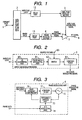
- Fig. 1 is a block diagram showing the structure of main parts of a transmitter according to a first embodiment of the present invention.
- the transmitter of the first embodiment comprises a transmit data input terminal 1, an amplitude phase extracting part (corresponding to an amplitude phase extracting unit) 2, an amplitude modulating part (corresponding to an amplitude modulating unit) 3, a phase modulating part (corresponding to a phase modulating unit) 4, a non-linear amplifying part (corresponding to a high frequency amplifying unit) 5, a transmit output terminal 6 and delay parts (corresponding to delay units) 12 and 13.
- the transmitter of this embodiment is characterized in that the delay part 12 is provided in a pre-stage of the amplitude modulating part 3 and the delay part 13 is provided in a pre-stage of the phase modulating part 4, respectively.
- amplitude data and phase data are extracted and outputted in the amplitude phase extracting part 2.
- the amplitude data outputted from the amplitude phase extracting part 2 is delayed by a prescribed quantity of delay in the delay part 12.
- an amplitude modulating signal obtained by modulating an amplitude in the amplitude modulating part 3 is inputted to the non-linear amplifying part 5 as a source voltage value.
- the phase data outputted from the amplitude phase extracting part 2 is delayed by a prescribed quantity of delay in the delay part 13.
- a phase modulating signal obtained by modulating a phase in the phase modulating part 4 is supplied to the non-linear amplifying part 5 as an input signal.
- the non-linear amplifying part 5 has a semiconductor amplifying element to form a high frequency amplifier.
- the phase modulating signal from the phase modulating part 4 is multiplied by the amplitude modulating signal from the amplitude modulating part 3 as the source voltage value to output an RF signal with a prescribed gain amplified from the transmit output terminal 6.
- the input signal to the non-linear amplifying part 5 is a signal of a prescribed envelope level, a non-linear amplifier having a good efficiency as the high frequency amplifier can be formed.
- Fig. 2 is a block diagram showing a structural example of the amplitude modulating part 3 in Fig. 1 .
- the amplitude modulating part 3 includes a DA (digital-analog) converting part 60, a pulse width modulating part 61, a switch 62, a source voltage input terminal 63 and a low-pass filter 64.
- the DA converting part 60, the pulse width modulating part 61, the switch 62 and the low-pass filter 64 are connected in order and in series.
- source voltage is inputted from the source voltage input terminal 63.
- the amplitude data having a digital value is converted to an analog signal in the DA converting part 60 and the pulse width of the analog signal is modulated in the pulse width modulating part 61.
- the switch 62 is switched in accordance with the pulse output of the pulse width modulating part 61.
- the output of the switch 62 is smoothed in the low-pass filter 64 to become the amplitude modulating signal and the amplitude modulating signal is applied to the non-linear amplifying part 5 as the source voltage.
- Fig. 3 is a block diagram showing a structural example of the phase modulating part 4 in Fig. 1 .
- the phase modulating part 4 includes a phase frequency comparing part 70, a low-pass filter 71, a voltage control oscillator (VCO) 72, a frequency dividing part 73 and a ⁇ (delta sigma) modulating part 74.
- VCO voltage control oscillator
- the phase modulating part 4 has a structure using a PLL (Phase-Locked Loop)in which the PLL that the phase frequency comparing part 70, the low pass filter 71 and the voltage control oscillator 72 are connected in order and in series and a part of the output of the voltage control oscillator 72 is fed back to the phase frequency comparing part 70 as a feedback signal through the frequency divider 73 is provided. Further, to the frequency divider 73, the output of the ⁇ (delta sigma) modulating part 74 is inputted.
- PLL Phase-Locked Loop
- the frequency of a signal obtained by dividing the frequency of the output of the voltage control oscillator 72 by the frequency divider 73 is compared with a reference frequency in the phase frequency comparing part 70 to output a difference between both the frequencies.
- the output of the phase frequency comparing part 70 becomes the control voltage of the voltage control oscillator 72 through the low-pass filter 71 and the output of the voltage control oscillator 72 is locked by a prescribed phase and frequency.
- the frequency dividing ratio of the frequency divider 73 is changed in accordance with a signal obtained by performing a delta sigma modulation to the phase data in the delta sigma modulating part 74.
- a phase modulation can be applied to the output of the voltage control oscillator 72.
- the amplitude modulating part 3 has a delay generated in the amplitude modulating signal mainly by the low-pass filter 64.
- the phase modulating part 4 has a delay generated in the phase modulating signal mainly by the low-pass filter 71. Accordingly, a relative discrepancy is generated between an amplitude and a phase due to the difference in quantity of delay between the amplitude modulating part 3 and the phase modulating part 4.
- the delay parts 12 and 13 are respectively provided in an amplitude signal path and a phase signal path.
- the quantity of delay of the delay part 12 of the amplitude signal path is set to zero and the quantity of delay of the delay part 13 of the phase signal path is adjusted.
- the quantity of delay of the amplitude signal path is allowed to correspond to the quantity of delay of the phase signal path. In such a way, a distortion due to the delay of the amplitude modulating signal can be reduced.
- the quantity of delay of the delay part 13 of the phase signal path is set to zero and the quantity of delay of the delay part 12 of the amplitude signal path is adjusted.
- the quantity of delay of the phase signal path is allowed to correspond to the quantity of delay of the amplitude signal path. In such a way, a distortion due to the delay of the phase modulating signal can be reduced.
- the quantity of delay of either of the delay parts 12 and 13 is set to zero.
- a rough adjustment may be performed by the quantity of delay of one of the phase signal path and the amplitude signal path and a fine adjustment may be performed by the quantity of delay of the other path.
- a method for setting a quantity of delay in accordance with the characteristics of a circuit upon design or a method for adjusting a quantity of delay to a suitable value for each of individuals upon production or the like may be employed.
- the delay part 12 is provided in a pre-stage of the amplitude modulating part 3 and the delay part 13 is provided in a pre-stage of the phase modulating part 4, respectively.
- the delay time of the amplitude signal path and the phase signal path can be adjusted and a distortion generated due to the difference in delay time between both the paths can be reduced.
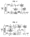
- Fig. 4 is a block diagram showing the structure of main parts of a transmitter according to a second embodiment of the present invention.
- the transmitter of the second embodiment includes a directional coupling part 7, an envelope detecting part (corresponding to an envelope detecting unit) 8, an AD converting part (analog-digital converting part) 9, an adding part 10 and an amplifying part 11 in addition to the structure of the first embodiment shown in Fig. 1 .
- Other structures are the same as those of the first embodiment and the same components are designated by the same reference numerals and the explanation thereof is omitted.
- an envelope component of an RF signal as the output of a non-linear amplifying part 5 is fed back in addition to the operation of the first embodiment.
- a part of a signal component of the output of the non-linear amplifying part 5 is allowed to branch by the directional coupling part 7 and inputted to the envelope detecting part 8 to detect the envelope signal of the RF signal.
- the detected envelope signal is converted to a digital signal in the AD converting part 9.
- the digital signal is negatively inverted and inputted to the adding part 10 as a negative component.
- the envelope component is subtracted from original amplitude data, and then, the obtained data is amplified to a prescribed level in the amplifying part 11 and inputted to an amplitude modulating part 3.
- a relative discrepancy is generated between an amplitude and a phase due to the difference in quantity of delay between the amplitude modulating part 3 and a phase modulating part 4 like the first embodiment.
- delay parts 12 and 13 are respectively provided in an amplitude signal path and a phase signal path. For instance, when a quantity of delay of the amplitude signal path is large, the quantity of delay of the delay part 12 of the amplitude signal path is set to zero and the quantity of delay of the delay part 13 of the phase signal path is adjusted. Thus, the quantity of delay of the amplitude signal path is allowed to correspond to the quantity of delay of the phase signal path. In such a way, a distortion due to the delay of an amplitude modulating signal can be reduced.
- the quantity of delay of the delay part 13 of the phase signal path is set to zero and the quantity of delay of the delay part 12 of the amplitude signal path is adjusted.
- the quantity of delay of the phase signal path is allowed to correspond to the quantity of delay of the amplitude signal path. In such a way, a distortion due to the delay of a phase modulating signal can be reduced.
- the quantity of delay of either of the delay parts 12 and 13 is set to zero.
- a rough adjustment may be performed by the quantity of delay of one of the phase signal path and the amplitude signal path and a fine adjustment may be performed by the quantity of delay of the other path.
- the delay part 12 is provided in a pre-stage of the amplitude modulating part 3 and the delay part 13 is provided in a pre-stage of the phase modulating part 4, respectively.
- the delay time of the amplitude signal path and the phase signal path can be adjusted and a distortion generated due to the difference in delay time between both the paths can be reduced.
- the loop gain of a negative feedback loop does not need to be increased.
- the loop gain of the negative feedback loop can be lowered to improve stability as a high frequency amplifier.
- Fig. 5 is a block diagram showing the structure of main parts of a transmitter according to a third embodiment of the present invention.
- the transmitter of the third embodiment includes a control signal input terminal 20 for inputting delay and signal path switching and control signals, a delay quantity switching and control part (corresponding to a delay quantity switching and control unit) 21, an amplitude data path switching part 22, a phase data path switching part 23, a second amplitude modulating part 24, a second non-linear amplifying art 25 and a second transmit output terminal 26 in addition to the structure of the first embodiment shown in Fig. 1 .
- Other structures are the same as those of the first embodiment and the same components are designated by the same reference numerals and the explanation thereof is omitted.
- a quantity of delay can be switched in addition to the operation of the first embodiment.
- the second amplitude modulating part 24 and the second non-linear amplifying part 25 are components for transmitting different transmit data from that of the first amplitude modulating part 3 and the first non-linear amplifying part 5 in the first embodiment.
- the signal bandwidth of transmit data is also different from that of the first embodiment.
- the structure of the second amplitude modulating part 24 is the same as that of the first embodiment shown in Fig.2 , however, the signal bandwidth of the transmit data is different.
- the cut-off frequency of the low-pass filter 64 is changed.
- the structure of a phase modulating part 4 is the same as that of the first embodiment shown in Fig. 3 , however, the cut-off frequency of the low-pass filter 71 is changed so as to meet the signal bandwidth of transmit data.
- the switches of the amplitude data path switching part 22 and the phase data path switching part 23 are switched so as to meet the bandwidth of the signal of employed transmit data by the delay quantity switching and control part 21.
- an amplitude signal path and a phase signal path are switched to use either the first amplitude modulating part 3 and the first non-linear amplifying part 5 or the second amplitude modulating part 24 and the second non-linear amplifying part 25.
- delay parts 12 and 13 are respectively provided in the amplitude signal path and the phase signal path.
- the quantity of delay of the delay part 12 of the amplitude signal path is set to zero and the quantity of delay of the delay part 13 of the phase signal path is adjusted.
- the quantity of delay of the amplitude signal path is allowed to correspond to the quantity of delay of the phase signal path. In such a way, a distortion due to the delay of an amplitude modulating signal can be reduced.
- the quantity of delay of the phase signal path is large, the quantity of delay of the delay part 13 of the phase signal path is set to zero and the quantity of delay of the delay part 12 of the amplitude signal path is adjusted.
- the quantity of delay of the phase signal path is allowed to correspond to the quantity of delay of the amplitude signal path. In such a way, a distortion due to the delay of a phase modulating signal can be reduced.
- the amplitude signal path and the phase signal path are switched by the delay quantity switching and control part 21 to adjust the quantity of delay of each path.
- a delay time can be adjusted in accordance with the bandwidth of the signal of the employed transmit data and a distortion due to a delay can be reduced.
- the quantity of delay of either of the delay parts 12 and 13 is set to zero.
- a rough adjustment may be performed by the quantity of delay of one of the phase signal path and the amplitude signal path and a fine adjustment may be performed by the quantity of delay of the other path.
- the delay quantity switching and control of the third embodiment may be applied to the structure of the second embodiment.
- the delay part 12 is provided in a pre-stage of the amplitude modulating part 3 and the delay part 13 is provided in a pre-stage of the phase modulating part 4, respectively.
- a quantity of delay is switched correspondingly to the switching of the transmit data.
- the delay time of the amplitude signal path and the phase signal path can be adjusted so as to meet the bandwidth of the signal of the transmit data.
- a distortion generated due to the difference in delay time between both the paths can be reduced.
- the delay quantity switching and control of the third embodiment is applied to the structure of the second embodiment, the delay time is adjusted to meet the bandwidth of the signal of the transmit data, so that the stability of a negative feedback loop can be improved.
- Fig. 6 is a block diagram showing the structure of main parts of a transmitter according to a fourth embodiment of the present invention.
- the transmitter of the fourth embodiment includes a delay quantity switching and control part 21, a switching signal input terminal 40 for inputting a delay quantity table data switching signal and a delay quantity table 41 in addition to the structure of the first embodiment shown in Fig.1 .
- Other structures are the same as those of the first embodiment and the same components are designated by the same reference numerals and the explanation thereof is omitted.
- a quantity of delay is switched by delay quantity data previously set and stored in the delay quantity table 41 in addition to the operation of the first embodiment.
- Corresponding delay quantity data is read and outputted from a plurality of delay quantities set and stored in the delay quantity table 41 in accordance with the delay quantity table data switching signal inputted to the switching signal input terminal 40.
- a quantity of delay in delay parts 12 and 13 is switched by the switching control part 21 on the basis of the delay quantity data.
- the delay quantity table 41 the delay quantity data corresponding to the operating state of the transmitter is stored. Thus, an optimum value of the quantity of delay in the operating state of the transmitter can be set.
- Fig. 7 shows one example of the delay quantity table 41.
- the delay quantity table 41 includes a data number 81, an operating state 82 of the transmitter and delay quantity data 83.
- the operating state 62 of the transmitter the operating states of the transmitter are stored.
- the delay quantity data 63 optimum delay quantity data corresponding to the operating states of the transmitter is stored.
- the quantity of delay of the delay part 12 of the amplitude signal path is set to zero and the quantity of delay of the delay part 13 of a phase signal path is adjusted.
- the quantity of delay of the amplitude signal path is allowed to correspond to the quantity of delay of the phase signal path. In such a way, a distortion due to the delay of an amplitude modulating signal can be reduced.
- the quantity of delay of the phase signal path is large, the quantity of delay of the delay part 13 of the phase signal path is set to zero and the quantity of delay of the delay part 12 of the amplitude signal path is adjusted.
- the quantity of delay of the phase signal path is allowed to correspond to the quantity of delay of the amplitude signal path. In such a way, a distortion due to the delay of a phase modulating signal can be reduced.
- the quantity of delay of either of the delay parts 12 and 13 is set to zero.
- a rough adjustment may be performed by the quantity of delay of one of the phase signal path and the amplitude signal path and a fine adjustment may be performed by the quantity of delay of the other path.
- the delay quantity switching and control of the fourth embodiment may be applied to the structure of the second embodiment or the third embodiment.
- the delay part 12 is provided in a pre-stage of an amplitude modulating part 3 and the delay part 13 is provided in a pre-stage of a phase modulating part 4, respectively.
- a quantity of delay is properly switched on the basis of the delay quantity data of the delay quantity table 41.
- the delay time of the amplitude signal path and the phase signal path can be respectively adjusted so as to obtain the quantity of delay corresponding to the state of the transmitter.
- a distortion generated due to the difference in delay time between both the paths can be reduced.
- the delay quantity switching and control of the fourth embodiment is applied to the structure of the second embodiment, the delay time is adjusted to meet the operating state of the transmitter, so that the stability of a negative feedback loop can be improved.
- the delay quantity switching and control of the fourth embodiment is applied to the structure of the third embodiment, even if transmit data is switched, the delay time can be adjusted to meet the bandwidth of the signal of the transmit data.
- Fig. 8 is a block diagram showing the structure of main parts of a transmitter according to a fifth embodiment of the present invention.
- an adjusting device including an RF signal measuring part (corresponding to a high frequency output measuring unit) 51 and a delay quantity calculating part (corresponding to a delay quantity calculating unit) 52 is connected to a transmitter 50 having the structure of the fourth embodiment shown in Fig. 7 .
- Other structures are the same as those of the fourth embodiment and the same components are designated by the same reference numerals and the explanation thereof is omitted.
- a method for adjusting a quantity of delay by using the adjusting device having the RF signal measuring part 51 and the delay quantity calculating part 52 will be illustrated.
- a modulation accuracy or the leakage power of adjacent channels or the like is measured by the RF signal measuring part 51.
- the characteristics such as the modulation accuracy or the leakage power of the adjacent channels are deteriorated due to the distortion of the output signal. Accordingly, a delay time is adjusted so that the difference in delay time between an amplitude signal path and a phase signal path, which causes the distortion of the output signal, is reduced on the basis of the measured results of the characteristics of an RF signal.
- the delay time of delay parts 12 and 13 is calculated by the delay quantity calculating part 52 so that the modulation accuracy or the leakage power of the adjacent channels has a desired value and stored in a delay quantity table. Then, delay quantity data stored in the delay quantity table 41 is read and outputted in accordance with the input of a delay quantity table data switching signal.
- the delay quantity data is stored by which the quantity of delay of the amplitude signal path is allowed to correspond to the quantity of delay of the phase signal path.
- the delay quantity data is stored by which the quantity of delay of the amplitude signal path is allowed to correspond to the quantity of delay of the phase signal path. In such a way, the delay quantity data is set so that a distortion generated due to the difference in delay between a phase modulating signal and an amplitude modulating signal can be reduced.
- the quantity of delay of either of the delay parts 12 and 13 is set to zero.
- a rough adjustment may be performed by the quantity of delay of one of the phase signal path and the amplitude signal path and a fine adjustment may be performed by the quantity of delay of the other path.
- a delay quantity adjusting function of the fifth embodiment may be applied to the structure of the third embodiment.
- a suitable delay quantity in which the distortion of the output signal of the transmitter is reduced can be calculated and set to the delay quantity table.
- the delay unit for adjusting the delay time of the amplitude signal path and the phase signal path is provided to adjust the delay time of both the paths to be equal.
- the distortion of the output of the transmitter generated due to the difference in delay time between both the paths can be reduced. Accordingly, in the transmitter, a high frequency power amplifier good in its power efficiency and capable of outputting a stable signal having little distortion can be realized.
- the transmitter having a good power efficiency and capable of outputting a stable signal with little distortion can be provided.
Abstract
Claims (4)
- Emetteur comprenant :une unité (2) d'extraction de phase d'amplitude, extrayant des données d'amplitude et des données de phase en provenance de données (1) de transmission entrées ;une unité (12;13) de retard, retardant au moins l'une parmi les données d'amplitude et les données de phase ;une unité (4) de modulation de phase, générant un signal à haute fréquence de phase modulée conformément aux données de phase ;une unité (3) de modulation d'amplitude, générant un signal de modulation d'amplitude conformément aux données d'amplitude ; etune unité (5) d'amplification de haute fréquence, générant un signal (6) de sortie à haute fréquence, en amplifiant la puissance du signal à haute fréquence de phase modulée, dans lequel une tension de source appliquée à l'unité (5) d'amplification à haute fréquence est commandée par le signal de modulation d'amplitude, de manière à ce que le signal (6) de sortie à haute fréquence soit modulé conformément aux données d'amplitude et aux données de phase,caractérisé par
une table (41) de quantité de retard, mémorisant des données (83) de quantité de retard présélectionnés conformément à l'état (82) de l'émetteur ; et
une unité (21) de commutation et de commande de quantité de retard, commutant et commandant la quantité de retard de l'unité (12;13) de retard en fonction des données (83) de quantité de retard de la table (41) de quantité de retard. - Emetteur selon la revendication 1, comprenant en plus :une unité (51) de mesure de sortie à haute fréquence, mesurant les caractéristiques du signal (6) de sortie à haute fréquence ; etune unité (52) de calcul de quantité de retard, calculant une quantité de retard prescrite en fonction d'un résultat mesuré de l'unité (51) de mesure de sortie à haute fréquence pour sélectionner la quantité de retard dans l'unité (12 ;13) de retard.
- Procédé destiné à régler un émetteur, comprenant les étapes consistant à :extraire des données d'amplitude et des données de phase en provenance des données (1) de transmission entrées ;retarder au moins l'une parmi les données d'amplitude et les données de phase ;générer un signal à haute fréquence de phase modulée, conformément aux données de phase ;générer un signal de modulation d'amplitude, conformément aux données d'amplitude ; etgénérer un signal (6) de sortie à haute fréquence en amplifiant la puissance du signal à haute fréquence de phase modulée, dans lequel l'étape d'amplification est commandée par le signal de modulation d'amplitude, de manière à ce que le signal (6) de sortie à haute fréquence soit modulé conformément aux données d'amplitude et aux données de phase,caractérisé par
la mémorisation des données (83) de quantité de retard présélectionnées conformément à l'état (82) de l'émetteur; et
la commutation et la commande de la quantité de retard de l'étape de retard, en fonction des données (83) de quantité de retard mémorisées. - Procédé selon la revendication 3, comprenant en plus les étapes consistant à :mesurer les caractéristiques du signal (6) de sortie à haute fréquence ; etcalculer une quantité de retard prescrite en fonction d'un résultat de l'étape de mesure, afin de sélectionner la quantité de retard dans l'étape de retard.
Applications Claiming Priority (3)
| Application Number | Priority Date | Filing Date | Title |
|---|---|---|---|
| JP2003029792A JP4230238B2 (ja) | 2003-02-06 | 2003-02-06 | 送信装置及びその調整方法 |
| JP2003029792 | 2003-02-06 | ||
| PCT/JP2004/001044 WO2004070959A1 (fr) | 2003-02-06 | 2004-02-03 | Dispositif de transmission et procede de reglage de celui-ci |
Publications (3)
| Publication Number | Publication Date |
|---|---|
| EP1598943A1 EP1598943A1 (fr) | 2005-11-23 |
| EP1598943A4 EP1598943A4 (fr) | 2006-07-12 |
| EP1598943B1 true EP1598943B1 (fr) | 2008-04-16 |
Family
ID=32844244
Family Applications (1)
| Application Number | Title | Priority Date | Filing Date |
|---|---|---|---|
| EP04707656A Expired - Fee Related EP1598943B1 (fr) | 2003-02-06 | 2004-02-03 | Dispositif de transmission et procede de reglage de celui-ci |
Country Status (6)
| Country | Link |
|---|---|
| US (1) | US7212791B2 (fr) |
| EP (1) | EP1598943B1 (fr) |
| JP (1) | JP4230238B2 (fr) |
| CN (1) | CN100418304C (fr) |
| DE (1) | DE602004013126T2 (fr) |
| WO (1) | WO2004070959A1 (fr) |
Families Citing this family (39)
| Publication number | Priority date | Publication date | Assignee | Title |
|---|---|---|---|---|
| JP3844352B2 (ja) * | 2003-08-07 | 2006-11-08 | 松下電器産業株式会社 | 送信装置 |
| US7372917B2 (en) * | 2004-08-25 | 2008-05-13 | Broadcom Corporation | Digital algorithm for on-line ACPR optimization in polar RF transmitters |
| JP4323968B2 (ja) * | 2004-01-14 | 2009-09-02 | 株式会社日立コミュニケーションテクノロジー | 無線通信装置のタイミング調整方法 |
| WO2005069503A1 (fr) * | 2004-01-16 | 2005-07-28 | Mitsubishi Denki Kabushiki Kaisha | Dispositif et procede d'alimentation |
| US7383027B2 (en) * | 2004-01-26 | 2008-06-03 | Matsushita Electric Industrial Co., Ltd. | Transmission circuit |
| US7359680B2 (en) * | 2004-09-14 | 2008-04-15 | Telefonaktiebolaget Lm Ericsson (Publ) | Delay calibration in polar modulation transmitters |
| JP2006135422A (ja) * | 2004-11-02 | 2006-05-25 | Matsushita Electric Ind Co Ltd | 送信回路 |
| JP2006203456A (ja) * | 2005-01-19 | 2006-08-03 | Matsushita Electric Ind Co Ltd | Eerシステム、及びeerシステムにおける遅延調整方法 |
| EP1845624B1 (fr) * | 2005-02-03 | 2012-01-11 | Panasonic Corporation | Emetteur et dispositif de transmission radio |
| US7400865B2 (en) | 2005-02-09 | 2008-07-15 | Nokia Corporation | Variable bandwidth envelope modulator for use with envelope elimination and restoration transmitter architecture and method |
| CN1943120B (zh) * | 2005-02-14 | 2010-10-20 | 松下电器产业株式会社 | 发送调制装置、通信设备以及移动无线设备 |
| JP4628142B2 (ja) * | 2005-03-03 | 2011-02-09 | パナソニック株式会社 | ポーラ変調送信装置、無線通信機及び電源電圧制御方法 |
| US7653147B2 (en) * | 2005-08-17 | 2010-01-26 | Intel Corporation | Transmitter control |
| US7496333B2 (en) * | 2005-12-13 | 2009-02-24 | Panasonic Corporation | Transmission circuit and communication apparatus employing the same |
| JP4652974B2 (ja) | 2005-12-27 | 2011-03-16 | 富士通株式会社 | タイミング調整装置及びタイミング調整方法 |
| US20070165708A1 (en) * | 2006-01-17 | 2007-07-19 | Hooman Darabi | Wireless transceiver with modulation path delay calibration |
| ATE515105T1 (de) | 2006-02-10 | 2011-07-15 | Nxp Bv | Leistungsverstärker |
| EP2037587B1 (fr) * | 2006-06-23 | 2015-01-07 | Panasonic Corporation | Circuit de transmission et dispositif de communication |
| US7570928B2 (en) * | 2006-08-04 | 2009-08-04 | Axiom Microdevices, Inc. | System and method for low delay corrective feedback power amplifier control |
| JP2008283678A (ja) * | 2007-04-11 | 2008-11-20 | Panasonic Corp | 送信回路、及び通信機器 |
| US7929926B2 (en) * | 2007-08-07 | 2011-04-19 | Harris Corporation | Transmitting RF signals employing both digital and analog components with a common amplifier |
| KR101201911B1 (ko) * | 2007-10-10 | 2012-11-20 | 삼성전자주식회사 | 무선통신 시스템에서 시간지연을 제어하여 전력증폭 장치 및 방법 |
| FI20075958A0 (fi) * | 2007-12-21 | 2007-12-21 | Nokia Corp | Lähetettävien signaalien prosessointi radiolähettimessä |
| JP2009260816A (ja) | 2008-04-18 | 2009-11-05 | Panasonic Corp | 振幅制御回路、ポーラ変調送信回路、及び、ポーラ変調方法 |
| US7932763B2 (en) * | 2009-04-02 | 2011-04-26 | Mediatek Inc. | Signal processing circuit and signal processing method |
| US8514969B2 (en) | 2009-06-11 | 2013-08-20 | Panasonic Corporation | Amplitude control circuit, polar modulation transmission circuit, and polar modulation method |
| WO2011004557A1 (fr) | 2009-07-07 | 2011-01-13 | パナソニック株式会社 | Circuit et procédé de transmission de modulation polaire |
| US8594589B2 (en) * | 2009-07-31 | 2013-11-26 | Nec Corporation | Power amplifier, power amplification method, and storage medium |
| JP5509935B2 (ja) * | 2010-03-03 | 2014-06-04 | 日本電気株式会社 | 電力増幅器およびその制御方法 |
| GB2479859B (en) * | 2010-03-30 | 2017-08-30 | Snaptrack Inc | Signal alignment for envelope tracking system |
| US20110319034A1 (en) * | 2010-06-28 | 2011-12-29 | Boe Eric N | Method and system for propagation time measurement and calibration using mutual coupling in a radio frequency transmit/receive system |
| CN102420631B (zh) * | 2011-11-04 | 2016-03-30 | 中兴通讯股份有限公司 | 功率放大装置、多模射频收发装置和多模终端 |
| EP3673930A1 (fr) | 2012-06-29 | 2020-07-01 | Cytosorbents Corporation | Procédés d'utilisation de polymères |
| GB2514388A (en) | 2013-05-22 | 2014-11-26 | Nujira Ltd | Delay adjustment |
| CN103336450B (zh) * | 2013-06-09 | 2015-07-29 | 广东宽普科技股份有限公司 | 一种基于功放自动测试系统的控制方法 |
| US9577771B1 (en) * | 2016-07-25 | 2017-02-21 | Apple Inc. | Radio frequency time skew calibration systems and methods |
| JP6625231B2 (ja) * | 2016-09-30 | 2019-12-25 | 三菱電機株式会社 | 光変調装置及び光変調装置のタイミング調整方法 |
| CN110300076B (zh) * | 2019-07-24 | 2022-05-31 | 南方科技大学 | Pam-4调制格式的前馈均衡器 |
| CN111030611A (zh) * | 2019-11-15 | 2020-04-17 | 安凯(广州)微电子技术有限公司 | 一种极坐标调制电路及其调制方法 |
Family Cites Families (24)
| Publication number | Priority date | Publication date | Assignee | Title |
|---|---|---|---|---|
| DE1284481B (de) * | 1965-10-14 | 1968-12-05 | Inst Lacznosci | System zur Unterdrueckung eines Seitenbandes bei Runfunksendern mit Amplitudenmodulation |
| US4176319A (en) * | 1975-12-04 | 1979-11-27 | Kahn Leonard R | Double sideband transmission system |
| US4194154A (en) | 1976-03-01 | 1980-03-18 | Kahn Leonard R | Narrow bandwidth network compensation method and apparatus |
| US5420536A (en) * | 1993-03-16 | 1995-05-30 | Victoria University Of Technology | Linearized power amplifier |
| FI105609B (fi) * | 1998-10-27 | 2000-09-15 | Nokia Mobile Phones Ltd | Menetelmä ja järjestely lähetyssignaalin muodostamiseksi |
| GB9825414D0 (en) * | 1998-11-19 | 1999-01-13 | Symbionics Limted | Linear RF power amplifier and transmitter |
| EP1035701A1 (fr) | 1999-03-08 | 2000-09-13 | Motorola, Inc. | Modulateur employant l'élimination et la restauration de l'enveloppe à tables de consultation |
| JP2000286915A (ja) * | 1999-03-31 | 2000-10-13 | Toshiba Corp | 信号変調回路及び信号変調方法 |
| GB2349994B (en) * | 1999-05-10 | 2003-06-04 | Intek Global Technologies Ltd | Apparatus for producing a radio-frequency signal |
| US6449465B1 (en) * | 1999-12-20 | 2002-09-10 | Motorola, Inc. | Method and apparatus for linear amplification of a radio frequency signal |
| US6366177B1 (en) | 2000-02-02 | 2002-04-02 | Tropian Inc. | High-efficiency power modulators |
| US6300826B1 (en) | 2000-05-05 | 2001-10-09 | Ericsson Telefon Ab L M | Apparatus and method for efficiently amplifying wideband envelope signals |
| JP3402363B2 (ja) * | 2000-06-13 | 2003-05-06 | 日本電気株式会社 | 送信ダイバーシチ方式送信機における遅延時間制御方式。 |
| GB2370435A (en) * | 2000-12-22 | 2002-06-26 | Nokia Mobile Phones Ltd | A polar loop transmitter for a mobile phone |
| US6735419B2 (en) * | 2001-01-18 | 2004-05-11 | Motorola, Inc. | High efficiency wideband linear wireless power amplifier |
| US6937668B2 (en) | 2001-03-28 | 2005-08-30 | Spectra Wireless, Inc. | Method of and apparatus for performing modulation |
| US6983025B2 (en) * | 2001-04-11 | 2006-01-03 | Tropian, Inc. | High quality power ramping in a communications transmitter |
| US7068984B2 (en) * | 2001-06-15 | 2006-06-27 | Telefonaktiebolaget Lm Ericsson (Publ) | Systems and methods for amplification of a communication signal |
| US6445249B1 (en) * | 2001-08-08 | 2002-09-03 | Motorola, Inc. | Modification of phase component of error signal to reduce variation of phase component of output signal of power amplifier |
| US6809588B2 (en) * | 2001-09-27 | 2004-10-26 | Hitachi Kokusai Electric Inc. | Distortion compensation circuit |
| US6600369B2 (en) * | 2001-12-07 | 2003-07-29 | Motorola, Inc. | Wideband linear amplifier with predistortion error correction |
| US6624712B1 (en) | 2002-06-11 | 2003-09-23 | Motorola, Inc. | Method and apparatus for power modulating to prevent instances of clipping |
| AU2003272918A1 (en) * | 2002-10-03 | 2004-04-23 | Matsushita Electric Industrial Co., Ltd. | Transmitting method and transmitter apparatus |
| JP4467319B2 (ja) * | 2004-01-29 | 2010-05-26 | 株式会社日立国際電気 | プリディストータ |
-
2003
- 2003-02-06 JP JP2003029792A patent/JP4230238B2/ja not_active Expired - Fee Related
-
2004
- 2004-02-03 EP EP04707656A patent/EP1598943B1/fr not_active Expired - Fee Related
- 2004-02-03 US US10/530,990 patent/US7212791B2/en not_active Expired - Fee Related
- 2004-02-03 DE DE602004013126T patent/DE602004013126T2/de not_active Expired - Lifetime
- 2004-02-03 CN CNB2004800011049A patent/CN100418304C/zh not_active Expired - Fee Related
- 2004-02-03 WO PCT/JP2004/001044 patent/WO2004070959A1/fr active IP Right Grant
Also Published As
| Publication number | Publication date |
|---|---|
| DE602004013126T2 (de) | 2009-07-02 |
| CN100418304C (zh) | 2008-09-10 |
| WO2004070959A1 (fr) | 2004-08-19 |
| JP2004266351A (ja) | 2004-09-24 |
| US20060009169A1 (en) | 2006-01-12 |
| US7212791B2 (en) | 2007-05-01 |
| EP1598943A4 (fr) | 2006-07-12 |
| EP1598943A1 (fr) | 2005-11-23 |
| DE602004013126D1 (de) | 2008-05-29 |
| JP4230238B2 (ja) | 2009-02-25 |
| CN1701521A (zh) | 2005-11-23 |
Similar Documents
| Publication | Publication Date | Title |
|---|---|---|
| EP1598943B1 (fr) | Dispositif de transmission et procede de reglage de celui-ci | |
| US7358829B2 (en) | Transmission apparatus, communication apparatus and mobile radio apparatus | |
| US7072626B2 (en) | Polar modulation transmitter | |
| US7062236B2 (en) | Transmitter circuits | |
| KR100372856B1 (ko) | 인접 채널 및 선택 채널 전력의 제어용 부하 조정을 갖는전력 증폭 회로 | |
| US6438360B1 (en) | Amplifier system with load control to produce an amplitude envelope | |
| US7792214B2 (en) | Polar modulation transmitter circuit and communications device | |
| KR101224247B1 (ko) | 전력 제어 폐루프 내의 공급 전압 제어된 전력 증폭기를위한 듀얼 전압 조정기 | |
| US7805115B1 (en) | Variable filter systems and methods for enhanced data rate communication systems | |
| US9143088B2 (en) | Control modules | |
| US8055215B2 (en) | Transmission circuit and communication device | |
| EP1923991A2 (fr) | Agencement de transmetteur et procédé de traitement du signal | |
| WO2004032345A1 (fr) | Procede d'emission et emetteur | |
| US7593480B2 (en) | Transmission device and radio communication device | |
| CN101558569A (zh) | 用于增强型数据速率gsm演进技术(edge)的极化环路发射器的振幅校准元件 | |
| EP2134053A3 (fr) | Transmetteurs numériques pour communication sans fil | |
| WO2006082894A1 (fr) | Emetteur et dispositif de transmission radio | |
| EP2378658A1 (fr) | Amplification de puissance à mode commuté | |
| US7400690B2 (en) | Adaptive phase controller, method of controlling a phase and transmitter employing the same | |
| US6690743B1 (en) | Compensation of delay in linearization loop of power amplifier | |
| US7209715B2 (en) | Power amplifying method, power amplifier, and communication apparatus | |
| WO2008099724A1 (fr) | Circuit de transmission linc et dispositif de communication utilisant ce circuit | |
| GB2386012A (en) | A linearized class C RF amplifier | |
| US7050770B1 (en) | Linearized amplifier having a bypass circuit | |
| Asbeck et al. | A polar linearisation system for RF power amplifiers |
Legal Events
| Date | Code | Title | Description |
|---|---|---|---|
| PUAI | Public reference made under article 153(3) epc to a published international application that has entered the european phase |
Free format text: ORIGINAL CODE: 0009012 |
|
| 17P | Request for examination filed |
Effective date: 20050414 |
|
| AK | Designated contracting states |
Kind code of ref document: A1 Designated state(s): AT BE BG CH CY CZ DE DK EE ES FI FR GB GR HU IE IT LI LU MC NL PT RO SE SI SK TR |
|
| AX | Request for extension of the european patent |
Extension state: AL LT LV MK |
|
| DAX | Request for extension of the european patent (deleted) | ||
| RBV | Designated contracting states (corrected) |
Designated state(s): DE FR GB |
|
| A4 | Supplementary search report drawn up and despatched |
Effective date: 20060613 |
|
| RIC1 | Information provided on ipc code assigned before grant |
Ipc: H03F 1/32 20060101ALI20060607BHEP Ipc: H03F 3/24 20060101ALN20060607BHEP Ipc: H04B 1/04 20060101AFI20040826BHEP Ipc: H03F 1/02 20060101ALI20060607BHEP |
|
| 17Q | First examination report despatched |
Effective date: 20061017 |
|
| GRAP | Despatch of communication of intention to grant a patent |
Free format text: ORIGINAL CODE: EPIDOSNIGR1 |
|
| GRAS | Grant fee paid |
Free format text: ORIGINAL CODE: EPIDOSNIGR3 |
|
| GRAA | (expected) grant |
Free format text: ORIGINAL CODE: 0009210 |
|
| AK | Designated contracting states |
Kind code of ref document: B1 Designated state(s): DE FR GB |
|
| REF | Corresponds to: |
Ref document number: 602004013126 Country of ref document: DE Date of ref document: 20080529 Kind code of ref document: P |
|
| ET | Fr: translation filed | ||
| RAP2 | Party data changed (patent owner data changed or rights of a patent transferred) |
Owner name: PANASONIC CORPORATION |
|
| PLBE | No opposition filed within time limit |
Free format text: ORIGINAL CODE: 0009261 |
|
| STAA | Information on the status of an ep patent application or granted ep patent |
Free format text: STATUS: NO OPPOSITION FILED WITHIN TIME LIMIT |
|
| 26N | No opposition filed |
Effective date: 20090119 |
|
| PGFP | Annual fee paid to national office [announced via postgrant information from national office to epo] |
Ref country code: FR Payment date: 20120221 Year of fee payment: 9 |
|
| PGFP | Annual fee paid to national office [announced via postgrant information from national office to epo] |
Ref country code: DE Payment date: 20120131 Year of fee payment: 9 |
|
| PGFP | Annual fee paid to national office [announced via postgrant information from national office to epo] |
Ref country code: GB Payment date: 20120201 Year of fee payment: 9 |
|
| GBPC | Gb: european patent ceased through non-payment of renewal fee |
Effective date: 20130203 |
|
| REG | Reference to a national code |
Ref country code: FR Ref legal event code: ST Effective date: 20131031 |
|
| REG | Reference to a national code |
Ref country code: DE Ref legal event code: R119 Ref document number: 602004013126 Country of ref document: DE Effective date: 20130903 |
|
| PG25 | Lapsed in a contracting state [announced via postgrant information from national office to epo] |
Ref country code: FR Free format text: LAPSE BECAUSE OF NON-PAYMENT OF DUE FEES Effective date: 20130228 Ref country code: GB Free format text: LAPSE BECAUSE OF NON-PAYMENT OF DUE FEES Effective date: 20130203 Ref country code: DE Free format text: LAPSE BECAUSE OF NON-PAYMENT OF DUE FEES Effective date: 20130903 |