EP1596267A1 - Circuit et méthode de protection pour régulateur de tension utilisant un signal de retroaction - Google Patents
Circuit et méthode de protection pour régulateur de tension utilisant un signal de retroaction Download PDFInfo
- Publication number
- EP1596267A1 EP1596267A1 EP05008414A EP05008414A EP1596267A1 EP 1596267 A1 EP1596267 A1 EP 1596267A1 EP 05008414 A EP05008414 A EP 05008414A EP 05008414 A EP05008414 A EP 05008414A EP 1596267 A1 EP1596267 A1 EP 1596267A1
- Authority
- EP
- European Patent Office
- Prior art keywords
- feedback
- voltage
- integrated circuit
- output
- terminal
- Prior art date
- Legal status (The legal status is an assumption and is not a legal conclusion. Google has not performed a legal analysis and makes no representation as to the accuracy of the status listed.)
- Granted
Links
Images

Classifications
-
- H—ELECTRICITY
- H02—GENERATION; CONVERSION OR DISTRIBUTION OF ELECTRIC POWER
- H02M—APPARATUS FOR CONVERSION BETWEEN AC AND AC, BETWEEN AC AND DC, OR BETWEEN DC AND DC, AND FOR USE WITH MAINS OR SIMILAR POWER SUPPLY SYSTEMS; CONVERSION OF DC OR AC INPUT POWER INTO SURGE OUTPUT POWER; CONTROL OR REGULATION THEREOF
- H02M1/00—Details of apparatus for conversion
- H02M1/08—Circuits specially adapted for the generation of control voltages for semiconductor devices incorporated in static converters
-
- G—PHYSICS
- G05—CONTROLLING; REGULATING
- G05F—SYSTEMS FOR REGULATING ELECTRIC OR MAGNETIC VARIABLES
- G05F1/00—Automatic systems in which deviations of an electric quantity from one or more predetermined values are detected at the output of the system and fed back to a device within the system to restore the detected quantity to its predetermined value or values, i.e. retroactive systems
- G05F1/10—Regulating voltage or current
- G05F1/46—Regulating voltage or current wherein the variable actually regulated by the final control device is dc
- G05F1/613—Regulating voltage or current wherein the variable actually regulated by the final control device is dc using semiconductor devices in parallel with the load as final control devices
Definitions
- An aspect of this invention relates to power systems for electronic circuits.
- a typical voltage regulator includes a feedback signal extending from the power input to the system back to the DC/DC converter.
- the feedback signal is used in the voltage regulator to regulate the output power at the input to the system, thereby reducing error in the regulated output that might be caused by conduction losses between the voltage regulator and the system.
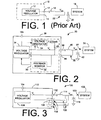
- FIG. 1 shows a typical conventional feedback system used with a voltage regulator 12 and electronic system 14.
- An integrated circuit 16 may include the voltage regulator 12 and connect via a pin 17 to external filter components such as an output inductor 18 and output capacitor 20.
- a feedback signal 22 from the regulated output, Vout may connect to the voltage regulator via a pin 19.
- the feedback signal 22 is typically received from a junction of the output inductor 18 and the output capacitor 20 so that gain and phase associated with the filter components is included within the control loop of the voltage regulator 12.
- the feedback signal may additionally be obtained from a point nearer to the input to the electronic system 14 to minimize the error caused by parasitic effects such as conduction losses and leakage inductance.
- An integrated circuit comprising a feedback terminal to receive a feedback signal.
- a voltage regulator has a feedback input to receive the feedback signal from the feedback terminal.
- the voltage regulator has a power output in communication with an output terminal. The voltage regulator being responsive to the feedback signal, to generate the power output.
- a voltage generator to generate a pull-up voltage having an amplitude greater than a DC voltage amplitude of the power output. The pull-up voltage being derived separately from the power output.
- a pull-up resistor in communication with the pull-up generator and the feedback input of the voltage regulator.
- FIG. 1 is a block diagram of an aspect of a conventional power supply feedback system.
- FIG. 2 is a block diagram of a power distribution system that includes an aspect of a feedback protection system.
- FIG. 4 is a block diagram of a power distribution system that includes another aspect of a feedback protection system.
- FIG. 2 shows a block diagram of an aspect of a power distribution system 30 for supplying a regulated output voltage, Vout, to a system 35 such as an electronic system.
- the power distribution system 30 includes a feedback protection system 50 to protect the power distribution system 30 from the potential effects of a feedback line 32 that is electrically degraded from normal operation, wherein electrically degraded is defined as having an increased impedance that causes a feedback signal on the feedback line 32 to be of insufficient quality for the control loop of the power distribution system 30 to control the regulated output voltage.
- the increased impedance of the feedback line 32 may be due to any cause such as a cold solder joint, the feedback line 32 being partially disconnected from the regulated output voltage, and the feedback line 32 being completely disconnected from the regulated output voltage.
- a voltage regulator 34 may generate the regulated output voltage, Vout, from an input voltage, Vin, and supply that regulated output voltage to the system 35.
- the voltage regulator 34 may be any type of voltage regulator such as switching regulators and linear regulators.
- An integrated circuit 36 may include the voltage regulator 34 and connect via one or more output terminals 38 to external filter components such as an output inductor 40 and output capacitor 42. Any type of terminals may be used for the output terminals 38 such as pins, ball grid arrays, and connectors.
- the voltage regulator 34 may generate a power output, Vc, that is filtered by the external filter components to generate Vout.
- the power output, Vc may be any type of power output to be used for powering the system 35 such as a chopped output of a switching regulator that is filtered by the external filter components, and a DC output from either a switching regulator or a linear regulator.
- the feedback line 32 may connect from the regulated output, Vout, to the voltage regulator via one or more feedback terminals 44. Any type of terminals may be used for the feedback terminals 44 such as pins, ball grid arrays, and connectors.
- a feedback signal carried on the feedback line 32 may be sensed at a junction of the output inductor 40 and the output capacitor 42 such as near an input 37 to the system 35.
- the integrated circuit 36 may include a feedback protection system to protect the system 35 if the feedback line 32 is electrically degraded.
- the feedback protection system 50 may monitor the feedback line 32 and detect if feedback line 32 is electrically degraded.
- the feedback protection system 50 may include a pull-up resistor 46 connected between the feedback line 32 and a pull-up voltage.
- the pull-up resistor 46 may apply the pull-up voltage through the relatively high impedance of the pull-up resistor 46 to the feedback line 32.
- the pull-up resistor 46 advantageously causes the output voltage to decrease if the feedback line 32 is electrically degraded.
- the feedback protection circuit 50 may advantageously operate if the feedback line 32 is electrically degraded to cause the control loop of the voltage regulator 32 to decrease the output voltage instead of relying on a overvoltage protection circuit. In addition, the feedback protection circuit 50 may cause the output voltage to decrease without first increasing.
- the pull-up voltage that is applied through the pull-up resistor 46 is high enough to cause the overvoltage circuit in the voltage regulator 34 to trigger an overvoltage shutdown of the voltage regulator 34 causing the output voltage to decrease to approximately zero volts.
- the overvoltage circuit operates to shutdown the voltage regulator 34 if the feedback line 32 is electrically degraded, the output voltage does not initially increase, but instead initially decreases.
- the shutdown circuit eventually causes the voltage regulator 34 to shutdown, the initial decrease in the output voltage may be due to operation of either the control loop or the overprotection circuit depending on their relative speed of operation.
- the pull-up resistor 46 may be any suitable resistance to pull-up the feedback line 32 to approximately the pull-up voltage if the feedback line 32 is electrically degraded. Exemplary values of the resistance may range from approximately 100 ohms to 1Meg ohms, although the resistance may be greater than or less than this range depending on several design factors such as the differential between the pull-up voltage and the output voltage, and the impedance of interface circuits that connect to the pull-up resistor 46. Although only a single pull-up resistor 46 is shown, another pull-up resistor may be coupled to a feedback return line if differential feedback sensing is employed.
- a feedback monitor 56 may monitor the feedback line 32 within the integrated circuit 50 to detect if the portion of the feedback line 32 extending from the regulated output voltage through the feedback terminal 44 is electrically degraded.
- the feedback monitor 56 may communicate a feedback degraded signal to the voltage regulator 34 to indicate that the feedback line 32 has an increased impedance.
- the feedback monitor 56 may compare the voltage on a portion of the feedback line 32 internal to the integrated circuit 36 to a reference voltage to determine if the feedback line 32 is electrically degraded.
- Figure 3 shows an aspect of a power distribution system 100 for supplying a regulated output voltage, Vout, to a system 102 such as an electronic system.
- the power distribution system 100 includes a feedback protection system 104 to protect the power distribution system 100 from the potential effects of a feedback line 106 that is electrically degraded from normal operation, wherein electrically degraded is defined as having an increased impedance that causes a feedback signal on the feedback line 106 to be of insufficient quality for the control loop of the power distribution system 100 to control the regulated output voltage.
- the increased impedance of the feedback line 106 may be due to any cause such as a cold solder joint, the feedback line 106 being partially disconnected from the regulated output voltage, and the feedback line 106 being completely disconnected from the regulated output voltage..
- a voltage regulator 108 may generate the regulated output voltage, Vout, from an input voltage, Vin, and supply that regulated output voltage to the system 102.
- the voltage regulator 108 may be any type of voltage regulator such as switching regulators and linear regulators.
- An integrated circuit 110 may include the voltage regulator 108 and connect via one or more output terminals 112 to external filter components such as an output inductor 114 and output capacitor 116.
- the voltage regulator 108 may generate a power output, Vc, that is filtered by the external filter components to generate Vout.
- the power output, Vc may be any type of power output to be used for powering the system 35 such as a chopped output of a switching regulator that is filtered by the external filter components, and a DC output from either a switching regulator or a linear regulator.
- Multiple feedback lines 106 may connect from the regulated output, Vout, to the voltage regulator via two or more feedback terminals 118.
- a feedback signal carried on the feedback lines 106 may be sensed at a junction of the output inductor 114 and the output capacitor 116 such as near an input 120 to the system 102.
- the feedback protection system 104 may comprise the feedback terminals 118 and interconnection of the feedback terminals 118 within the integrated circuit 110.
- the feedback protection system 104 advantageously provides redundant feedback lines 106 and feedback terminals 118 to prevent the electrical degradation of any one of the feedback lines from affecting the operation of the voltage regulator 108.
- the signal generator 254 may be any type of source including an alternating current (AC) source and a direct current (DC) source.
- a tone detector may monitor the feedback input of the voltage regulator 234 to detect an AC signal from the AC source, which indicates a degraded electrical condition of the feedback line 232 and feedback terminal 244.
- the feedback monitor 256 may comprise the tone detector.
Priority Applications (2)
| Application Number | Priority Date | Filing Date | Title |
|---|---|---|---|
| EP05011613A EP1602998A1 (fr) | 2004-05-13 | 2005-04-18 | Régulateur de tension avec rétroaction multiple |
| EP05011612A EP1602997B1 (fr) | 2004-05-13 | 2005-04-18 | Régulateur de tension avec générateur de signaux à haute impédance de sortie |
Applications Claiming Priority (2)
| Application Number | Priority Date | Filing Date | Title |
|---|---|---|---|
| US846717 | 2004-05-13 | ||
| US10/846,717 US7514911B2 (en) | 2004-05-13 | 2004-05-13 | Voltage regulator feedback protection method and apparatus |
Related Child Applications (2)
| Application Number | Title | Priority Date | Filing Date |
|---|---|---|---|
| EP05011612A Division EP1602997B1 (fr) | 2004-05-13 | 2005-04-18 | Régulateur de tension avec générateur de signaux à haute impédance de sortie |
| EP05011613A Division EP1602998A1 (fr) | 2004-05-13 | 2005-04-18 | Régulateur de tension avec rétroaction multiple |
Publications (2)
| Publication Number | Publication Date |
|---|---|
| EP1596267A1 true EP1596267A1 (fr) | 2005-11-16 |
| EP1596267B1 EP1596267B1 (fr) | 2008-10-15 |
Family
ID=34935311
Family Applications (3)
| Application Number | Title | Priority Date | Filing Date |
|---|---|---|---|
| EP05011613A Ceased EP1602998A1 (fr) | 2004-05-13 | 2005-04-18 | Régulateur de tension avec rétroaction multiple |
| EP05008414A Expired - Fee Related EP1596267B1 (fr) | 2004-05-13 | 2005-04-18 | Circuit et méthode de protection pour régulateur de tension utilisant un signal de retroaction |
| EP05011612A Expired - Fee Related EP1602997B1 (fr) | 2004-05-13 | 2005-04-18 | Régulateur de tension avec générateur de signaux à haute impédance de sortie |
Family Applications Before (1)
| Application Number | Title | Priority Date | Filing Date |
|---|---|---|---|
| EP05011613A Ceased EP1602998A1 (fr) | 2004-05-13 | 2005-04-18 | Régulateur de tension avec rétroaction multiple |
Family Applications After (1)
| Application Number | Title | Priority Date | Filing Date |
|---|---|---|---|
| EP05011612A Expired - Fee Related EP1602997B1 (fr) | 2004-05-13 | 2005-04-18 | Régulateur de tension avec générateur de signaux à haute impédance de sortie |
Country Status (6)
| Country | Link |
|---|---|
| US (2) | US7514911B2 (fr) |
| EP (3) | EP1602998A1 (fr) |
| JP (3) | JP4712429B2 (fr) |
| CN (3) | CN1696859B (fr) |
| DE (2) | DE602005019946D1 (fr) |
| TW (3) | TWI370341B (fr) |
Cited By (1)
| Publication number | Priority date | Publication date | Assignee | Title |
|---|---|---|---|---|
| WO2021026866A1 (fr) | 2019-08-15 | 2021-02-18 | Tridonic Gmbh & Co Kg | Procédé d'identification de charge de sortie et appareil l'incorporant |
Families Citing this family (8)
| Publication number | Priority date | Publication date | Assignee | Title |
|---|---|---|---|---|
| US20110298432A1 (en) | 2010-06-07 | 2011-12-08 | Skyworks Solutions, Inc | Apparatus and method for variable voltage function |
| US8988140B2 (en) | 2013-06-28 | 2015-03-24 | International Business Machines Corporation | Real-time adaptive voltage control of logic blocks |
| JP2016181071A (ja) * | 2015-03-24 | 2016-10-13 | 日立オートモティブシステムズ株式会社 | 電源装置 |
| KR102163054B1 (ko) * | 2015-09-15 | 2020-10-08 | 삼성전기주식회사 | 신호 생성 장치 |
| CN107678482B (zh) * | 2017-09-12 | 2020-04-03 | 郑州云海信息技术有限公司 | 一种电压调节的装置及调节方法 |
| WO2019244374A1 (fr) * | 2018-06-22 | 2019-12-26 | ローム株式会社 | Source d'alimentation à découpage, dispositif à circuit intégré à semi-conducteur et circuit d'entrée différentielle |
| CN111130328B (zh) * | 2018-10-31 | 2021-12-28 | 瑞昱半导体股份有限公司 | 介面电路以及控制介面电路内的开关电路的方法 |
| CN114337297A (zh) * | 2021-12-15 | 2022-04-12 | 珠海格力电器股份有限公司 | 一种开关电源的反馈电路、开关电源及用电设备 |
Citations (3)
| Publication number | Priority date | Publication date | Assignee | Title |
|---|---|---|---|---|
| US5508603A (en) * | 1995-03-28 | 1996-04-16 | Northrop Grumman Corporation | Polarity corrected, intermittent compensated, remote load voltage regulation |
| US5672958A (en) * | 1995-11-14 | 1997-09-30 | Dell Usa L.P. | Method and apparatus for modifying feedback sensing for a redundant power supply system |
| EP0823681A2 (fr) * | 1996-07-31 | 1998-02-11 | Data General Corporation | Commutateur à démarrage doux avec régulation de tension et limitation de courant |
Family Cites Families (30)
| Publication number | Priority date | Publication date | Assignee | Title |
|---|---|---|---|---|
| US3769568A (en) * | 1972-07-31 | 1973-10-30 | Bell Telephone Labor Inc | Dc-to-dc converter having soft start and other regulation features employing priority of pulse feedback |
| US4621313A (en) * | 1985-06-28 | 1986-11-04 | Zenith Electronics Corporation | Soft-start capacitor discharge circuit |
| JPH0331531A (ja) * | 1989-06-27 | 1991-02-12 | Nissan Motor Co Ltd | 内燃機関のスロットル弁制御装置 |
| IE75374B1 (en) * | 1989-11-13 | 1997-09-10 | Nat Csf Corp | Uninterruptible power supply |
| JPH0655295B2 (ja) | 1990-06-27 | 1994-07-27 | 新日本製鐵株式会社 | 耐食性,溶接性,潤滑性,連続パンチ打抜き性,上塗り塗装性に優れた表面処理鋼板及びその製造方法 |
| JP2545533Y2 (ja) * | 1990-10-04 | 1997-08-25 | 株式会社リコー | レーザダイオード制御回路 |
| US5204809A (en) | 1992-04-03 | 1993-04-20 | International Business Machines Corporation | H-driver DC-to-DC converter utilizing mutual inductance |
| US5408173A (en) * | 1992-10-01 | 1995-04-18 | Kronos Incorporated | Manual-adjustment-free controlled-voltage and current-limited D.C. voltage supply |
| JP3426342B2 (ja) * | 1994-06-03 | 2003-07-14 | 日本アビオニクス株式会社 | 溶接電源 |
| US5530636A (en) | 1995-01-13 | 1996-06-25 | Dell Usa, L.P. | Automatic feedback system for a dual output power supply |
| JP3349897B2 (ja) * | 1995-08-11 | 2002-11-25 | 富士通株式会社 | 直流−直流変換装置 |
| US6046896A (en) | 1995-08-11 | 2000-04-04 | Fijitsu Limited | DC-to-DC converter capable of preventing overvoltage |
| JPH0984342A (ja) * | 1995-09-18 | 1997-03-28 | Ricoh Co Ltd | 電源装置 |
| US5894243A (en) * | 1996-12-11 | 1999-04-13 | Micro Linear Corporation | Three-pin buck and four-pin boost converter having open loop output voltage control |
| SE520359C2 (sv) * | 1997-03-06 | 2003-07-01 | Ericsson Telefon Ab L M | Elektrisk krets för att kompensera oönskat spänningsbortfall i en ledare |
| JPH10248252A (ja) * | 1997-03-07 | 1998-09-14 | Meidensha Corp | コンデンサの充電装置 |
| SE509679C2 (sv) * | 1997-04-10 | 1999-02-22 | Ericsson Telefon Ab L M | Förfarande för att styra en likspänning från en DC-DC- omvandlare och en DC-DC-omvandlare |
| US5834925A (en) * | 1997-05-08 | 1998-11-10 | Cisco Technology, Inc. | Current sharing power supplies with redundant operation |
| US5867013A (en) * | 1997-11-20 | 1999-02-02 | Cypress Semiconductor Corporation | Startup circuit for band-gap reference circuit |
| JPH11249750A (ja) * | 1998-03-02 | 1999-09-17 | Minolta Co Ltd | 電子機器 |
| US5977757A (en) | 1998-11-02 | 1999-11-02 | Hewlett-Packard Company | Power supply having automatic voltage sensing |
| US6301133B1 (en) | 1999-04-07 | 2001-10-09 | Astec International Limited | Power supply system with ORing element and control circuit |
| CN1312493A (zh) * | 2000-02-07 | 2001-09-12 | 精工电子有限公司 | 半导体集成电路 |
| JP2001359273A (ja) * | 2000-06-14 | 2001-12-26 | Toshiba Corp | 電源装置及びこの電源装置を有する情報処理装置 |
| US6362986B1 (en) | 2001-03-22 | 2002-03-26 | Volterra, Inc. | Voltage converter with coupled inductive windings, and associated methods |
| JP3595532B2 (ja) | 2001-10-18 | 2004-12-02 | Smk株式会社 | 半導体レーザの駆動制御装置 |
| US6958552B2 (en) | 2002-04-10 | 2005-10-25 | Adc Dsl Systems, Inc. | Failsafe power oring with current sharing |
| CN2553414Y (zh) * | 2002-07-05 | 2003-05-28 | 北京通力环电气股份有限公司 | Pwm型高频开关电源恒压/恒流控制器 |
| US6772011B2 (en) | 2002-08-20 | 2004-08-03 | Thoratec Corporation | Transmission of information from an implanted medical device |
| KR100594872B1 (ko) | 2002-10-04 | 2006-06-30 | 롬 씨오.엘티디 | 전압귀환회로를 갖는 반도체 장치 및 이를 이용한 전자장치 |
-
2004
- 2004-05-13 US US10/846,717 patent/US7514911B2/en active Active
-
2005
- 2005-04-18 EP EP05011613A patent/EP1602998A1/fr not_active Ceased
- 2005-04-18 DE DE602005019946T patent/DE602005019946D1/de active Active
- 2005-04-18 DE DE602005010325T patent/DE602005010325D1/de active Active
- 2005-04-18 EP EP05008414A patent/EP1596267B1/fr not_active Expired - Fee Related
- 2005-04-18 EP EP05011612A patent/EP1602997B1/fr not_active Expired - Fee Related
- 2005-04-20 TW TW094132733A patent/TWI370341B/zh not_active IP Right Cessation
- 2005-04-20 TW TW094112632A patent/TWI388963B/zh not_active IP Right Cessation
- 2005-04-20 TW TW094132734A patent/TW200613942A/zh unknown
- 2005-04-25 JP JP2005126973A patent/JP4712429B2/ja not_active Expired - Fee Related
- 2005-04-29 CN CN200510067954.5A patent/CN1696859B/zh not_active Expired - Fee Related
- 2005-05-13 CN CN200510069369.9A patent/CN1702587B/zh not_active Expired - Fee Related
- 2005-05-13 CN CNA2005100752254A patent/CN1862437A/zh active Pending
- 2005-06-20 JP JP2005180009A patent/JP4712453B2/ja not_active Expired - Fee Related
- 2005-06-20 JP JP2005180008A patent/JP2006014590A/ja not_active Withdrawn
-
2009
- 2009-03-05 US US12/398,265 patent/US7960958B2/en active Active
Patent Citations (3)
| Publication number | Priority date | Publication date | Assignee | Title |
|---|---|---|---|---|
| US5508603A (en) * | 1995-03-28 | 1996-04-16 | Northrop Grumman Corporation | Polarity corrected, intermittent compensated, remote load voltage regulation |
| US5672958A (en) * | 1995-11-14 | 1997-09-30 | Dell Usa L.P. | Method and apparatus for modifying feedback sensing for a redundant power supply system |
| EP0823681A2 (fr) * | 1996-07-31 | 1998-02-11 | Data General Corporation | Commutateur à démarrage doux avec régulation de tension et limitation de courant |
Cited By (2)
| Publication number | Priority date | Publication date | Assignee | Title |
|---|---|---|---|---|
| WO2021026866A1 (fr) | 2019-08-15 | 2021-02-18 | Tridonic Gmbh & Co Kg | Procédé d'identification de charge de sortie et appareil l'incorporant |
| EP3999935A4 (fr) * | 2019-08-15 | 2022-08-17 | Tridonic GmbH & Co KG | Procédé d'identification de charge de sortie et appareil l'incorporant |
Also Published As
| Publication number | Publication date |
|---|---|
| EP1602997B1 (fr) | 2010-03-17 |
| US7960958B2 (en) | 2011-06-14 |
| US20090167275A1 (en) | 2009-07-02 |
| TW200613942A (en) | 2006-05-01 |
| DE602005010325D1 (de) | 2008-11-27 |
| JP4712453B2 (ja) | 2011-06-29 |
| JP2005327270A (ja) | 2005-11-24 |
| CN1696859A (zh) | 2005-11-16 |
| EP1602998A1 (fr) | 2005-12-07 |
| US7514911B2 (en) | 2009-04-07 |
| JP2006014590A (ja) | 2006-01-12 |
| TW200537268A (en) | 2005-11-16 |
| DE602005019946D1 (de) | 2010-04-29 |
| TWI370341B (en) | 2012-08-11 |
| JP2005354896A (ja) | 2005-12-22 |
| JP4712429B2 (ja) | 2011-06-29 |
| CN1862437A (zh) | 2006-11-15 |
| US20050253566A1 (en) | 2005-11-17 |
| TW200602833A (en) | 2006-01-16 |
| CN1702587A (zh) | 2005-11-30 |
| CN1696859B (zh) | 2010-06-02 |
| EP1596267B1 (fr) | 2008-10-15 |
| TWI388963B (zh) | 2013-03-11 |
| EP1602997A1 (fr) | 2005-12-07 |
| CN1702587B (zh) | 2010-04-14 |
Similar Documents
| Publication | Publication Date | Title |
|---|---|---|
| US7960958B2 (en) | Voltage regulator feedback protection method and apparatus | |
| US4743835A (en) | Output hold-up circuit for a step-up voltage regulator | |
| US4717833A (en) | Single wire current share paralleling of power supplies | |
| US8587150B2 (en) | Method and modular system for charging a battery | |
| RU2338262C2 (ru) | Двухпроводной передатчик с изолированным выходом can | |
| CA2575944C (fr) | Alimentation a resistances en echelle avec protection contre la surtension | |
| US7804195B2 (en) | Power supply system and protection method | |
| US20080055798A1 (en) | Electronic power protection circuit and applications thereof | |
| CN102035410B (zh) | 电压调节电路及具有该电压调节电路的电源适配器 | |
| US4609828A (en) | Single wire current share paralleling of power supplies | |
| CN101278471A (zh) | 用于两个直流电源的逆变器以及用于运行该逆变器的方法 | |
| US20050093523A1 (en) | Surge current suppression in power-factor-corrected AC-to-DC converter with capacitive load | |
| US20020070717A1 (en) | Apparatus and methods for boosting power supplied at a remote node | |
| CN109391024A (zh) | 备用供电设备及备用供电系统 | |
| CN216115893U (zh) | 扫描仪及扫描系统 | |
| US7023716B1 (en) | Precharging load capacitor for power-factor-corrected AC-to-DC power supply | |
| TW202046591A (zh) | 電力負載分配系統 | |
| CN219960389U (zh) | 电源控制电路及电源电路 | |
| CN111316555B (zh) | 电力变换装置以及发电系统 | |
| US7397262B2 (en) | Burn-in system power stage | |
| US20240120765A1 (en) | Integrated battery charge regulation circuit based on power fet conductivity modulation | |
| CN108233688B (zh) | 前摄工作的过压保护电路 | |
| KR100300812B1 (ko) | 유피에스에 있어서 고전압 검출회로 | |
| CN117435017A (zh) | 一种计算设备 | |
| CN114337190A (zh) | 一种输出电压补偿电路及补偿方法 |
Legal Events
| Date | Code | Title | Description |
|---|---|---|---|
| PUAI | Public reference made under article 153(3) epc to a published international application that has entered the european phase |
Free format text: ORIGINAL CODE: 0009012 |
|
| AK | Designated contracting states |
Kind code of ref document: A1 Designated state(s): AT BE BG CH CY CZ DE DK EE ES FI FR GB GR HU IE IS IT LI LT LU MC NL PL PT RO SE SI SK TR |
|
| AX | Request for extension of the european patent |
Extension state: AL BA HR LV MK YU |
|
| 17P | Request for examination filed |
Effective date: 20060512 |
|
| AKX | Designation fees paid |
Designated state(s): DE FR GB |
|
| 17Q | First examination report despatched |
Effective date: 20070220 |
|
| GRAP | Despatch of communication of intention to grant a patent |
Free format text: ORIGINAL CODE: EPIDOSNIGR1 |
|
| GRAS | Grant fee paid |
Free format text: ORIGINAL CODE: EPIDOSNIGR3 |
|
| GRAA | (expected) grant |
Free format text: ORIGINAL CODE: 0009210 |
|
| AK | Designated contracting states |
Kind code of ref document: B1 Designated state(s): DE FR GB |
|
| REG | Reference to a national code |
Ref country code: GB Ref legal event code: FG4D |
|
| REF | Corresponds to: |
Ref document number: 602005010325 Country of ref document: DE Date of ref document: 20081127 Kind code of ref document: P |
|
| PLBE | No opposition filed within time limit |
Free format text: ORIGINAL CODE: 0009261 |
|
| STAA | Information on the status of an ep patent application or granted ep patent |
Free format text: STATUS: NO OPPOSITION FILED WITHIN TIME LIMIT |
|
| 26N | No opposition filed |
Effective date: 20090716 |
|
| REG | Reference to a national code |
Ref country code: FR Ref legal event code: PLFP Year of fee payment: 12 |
|
| REG | Reference to a national code |
Ref country code: FR Ref legal event code: PLFP Year of fee payment: 13 |
|
| REG | Reference to a national code |
Ref country code: FR Ref legal event code: PLFP Year of fee payment: 14 |
|
| PGFP | Annual fee paid to national office [announced via postgrant information from national office to epo] |
Ref country code: DE Payment date: 20180427 Year of fee payment: 14 |
|
| PGFP | Annual fee paid to national office [announced via postgrant information from national office to epo] |
Ref country code: FR Payment date: 20180425 Year of fee payment: 14 |
|
| PGFP | Annual fee paid to national office [announced via postgrant information from national office to epo] |
Ref country code: GB Payment date: 20180427 Year of fee payment: 14 |
|
| REG | Reference to a national code |
Ref country code: DE Ref legal event code: R119 Ref document number: 602005010325 Country of ref document: DE |
|
| GBPC | Gb: european patent ceased through non-payment of renewal fee |
Effective date: 20190418 |
|
| PG25 | Lapsed in a contracting state [announced via postgrant information from national office to epo] |
Ref country code: GB Free format text: LAPSE BECAUSE OF NON-PAYMENT OF DUE FEES Effective date: 20190418 Ref country code: DE Free format text: LAPSE BECAUSE OF NON-PAYMENT OF DUE FEES Effective date: 20191101 |
|
| PG25 | Lapsed in a contracting state [announced via postgrant information from national office to epo] |
Ref country code: FR Free format text: LAPSE BECAUSE OF NON-PAYMENT OF DUE FEES Effective date: 20190430 |