EP1596235B1 - Projektionsbelichtungsanlage der Mikrolithographie mit passiver thermischer Kompensation - Google Patents
Projektionsbelichtungsanlage der Mikrolithographie mit passiver thermischer Kompensation Download PDFInfo
- Publication number
- EP1596235B1 EP1596235B1 EP05106797A EP05106797A EP1596235B1 EP 1596235 B1 EP1596235 B1 EP 1596235B1 EP 05106797 A EP05106797 A EP 05106797A EP 05106797 A EP05106797 A EP 05106797A EP 1596235 B1 EP1596235 B1 EP 1596235B1
- Authority
- EP
- European Patent Office
- Prior art keywords
- projection exposure
- exposure apparatus
- optical element
- microlithographic projection
- lens
- Prior art date
- Legal status (The legal status is an assumption and is not a legal conclusion. Google has not performed a legal analysis and makes no representation as to the accuracy of the status listed.)
- Expired - Lifetime
Links
- 230000003287 optical effect Effects 0.000 title claims description 35
- 238000001393 microlithography Methods 0.000 title description 4
- 238000001816 cooling Methods 0.000 claims description 23
- 239000000463 material Substances 0.000 claims description 18
- 230000005855 radiation Effects 0.000 claims description 6
- 238000000265 homogenisation Methods 0.000 claims description 3
- 210000001747 pupil Anatomy 0.000 claims 1
- 241000219739 Lens Species 0.000 description 36
- 230000000694 effects Effects 0.000 description 5
- 238000005286 illumination Methods 0.000 description 5
- 239000007789 gas Substances 0.000 description 4
- 240000004322 Lens culinaris Species 0.000 description 3
- 241000022563 Rema Species 0.000 description 3
- 229910052782 aluminium Inorganic materials 0.000 description 3
- XAGFODPZIPBFFR-UHFFFAOYSA-N aluminium Chemical compound [Al] XAGFODPZIPBFFR-UHFFFAOYSA-N 0.000 description 3
- 238000010438 heat treatment Methods 0.000 description 3
- 230000031700 light absorption Effects 0.000 description 3
- 238000000034 method Methods 0.000 description 3
- VYPSYNLAJGMNEJ-UHFFFAOYSA-N Silicium dioxide Chemical compound O=[Si]=O VYPSYNLAJGMNEJ-UHFFFAOYSA-N 0.000 description 2
- 238000004364 calculation method Methods 0.000 description 2
- 239000001307 helium Substances 0.000 description 2
- 229910052734 helium Inorganic materials 0.000 description 2
- SWQJXJOGLNCZEY-UHFFFAOYSA-N helium atom Chemical compound [He] SWQJXJOGLNCZEY-UHFFFAOYSA-N 0.000 description 2
- 229910052709 silver Inorganic materials 0.000 description 2
- 239000004332 silver Substances 0.000 description 2
- 238000004088 simulation Methods 0.000 description 2
- RYGMFSIKBFXOCR-UHFFFAOYSA-N Copper Chemical compound [Cu] RYGMFSIKBFXOCR-UHFFFAOYSA-N 0.000 description 1
- 239000006244 Medium Thermal Substances 0.000 description 1
- 239000006094 Zerodur Substances 0.000 description 1
- 238000010521 absorption reaction Methods 0.000 description 1
- 230000006978 adaptation Effects 0.000 description 1
- 239000000853 adhesive Substances 0.000 description 1
- 238000004026 adhesive bonding Methods 0.000 description 1
- 230000001070 adhesive effect Effects 0.000 description 1
- 230000004075 alteration Effects 0.000 description 1
- 230000001447 compensatory effect Effects 0.000 description 1
- 239000004020 conductor Substances 0.000 description 1
- 238000010276 construction Methods 0.000 description 1
- 230000001419 dependent effect Effects 0.000 description 1
- 238000011161 development Methods 0.000 description 1
- 230000018109 developmental process Effects 0.000 description 1
- 238000005516 engineering process Methods 0.000 description 1
- 238000003384 imaging method Methods 0.000 description 1
- 239000004973 liquid crystal related substance Substances 0.000 description 1
- 229910052751 metal Inorganic materials 0.000 description 1
- 239000002184 metal Substances 0.000 description 1
- 239000010453 quartz Substances 0.000 description 1
- 230000001105 regulatory effect Effects 0.000 description 1
- 238000007493 shaping process Methods 0.000 description 1
Images


Classifications
-
- G—PHYSICS
- G03—PHOTOGRAPHY; CINEMATOGRAPHY; ANALOGOUS TECHNIQUES USING WAVES OTHER THAN OPTICAL WAVES; ELECTROGRAPHY; HOLOGRAPHY
- G03F—PHOTOMECHANICAL PRODUCTION OF TEXTURED OR PATTERNED SURFACES, e.g. FOR PRINTING, FOR PROCESSING OF SEMICONDUCTOR DEVICES; MATERIALS THEREFOR; ORIGINALS THEREFOR; APPARATUS SPECIALLY ADAPTED THEREFOR
- G03F7/00—Photomechanical, e.g. photolithographic, production of textured or patterned surfaces, e.g. printing surfaces; Materials therefor, e.g. comprising photoresists; Apparatus specially adapted therefor
- G03F7/70—Microphotolithographic exposure; Apparatus therefor
- G03F7/70216—Mask projection systems
- G03F7/70358—Scanning exposure, i.e. relative movement of patterned beam and workpiece during imaging
-
- G—PHYSICS
- G02—OPTICS
- G02B—OPTICAL ELEMENTS, SYSTEMS OR APPARATUS
- G02B7/00—Mountings, adjusting means, or light-tight connections, for optical elements
- G02B7/02—Mountings, adjusting means, or light-tight connections, for optical elements for lenses
- G02B7/028—Mountings, adjusting means, or light-tight connections, for optical elements for lenses with means for compensating for changes in temperature or for controlling the temperature; thermal stabilisation
-
- G—PHYSICS
- G03—PHOTOGRAPHY; CINEMATOGRAPHY; ANALOGOUS TECHNIQUES USING WAVES OTHER THAN OPTICAL WAVES; ELECTROGRAPHY; HOLOGRAPHY
- G03F—PHOTOMECHANICAL PRODUCTION OF TEXTURED OR PATTERNED SURFACES, e.g. FOR PRINTING, FOR PROCESSING OF SEMICONDUCTOR DEVICES; MATERIALS THEREFOR; ORIGINALS THEREFOR; APPARATUS SPECIALLY ADAPTED THEREFOR
- G03F7/00—Photomechanical, e.g. photolithographic, production of textured or patterned surfaces, e.g. printing surfaces; Materials therefor, e.g. comprising photoresists; Apparatus specially adapted therefor
- G03F7/70—Microphotolithographic exposure; Apparatus therefor
- G03F7/70058—Mask illumination systems
- G03F7/70091—Illumination settings, i.e. intensity distribution in the pupil plane or angular distribution in the field plane; On-axis or off-axis settings, e.g. annular, dipole or quadrupole settings; Partial coherence control, i.e. sigma or numerical aperture [NA]
- G03F7/70108—Off-axis setting using a light-guiding element, e.g. diffractive optical elements [DOEs] or light guides
-
- G—PHYSICS
- G03—PHOTOGRAPHY; CINEMATOGRAPHY; ANALOGOUS TECHNIQUES USING WAVES OTHER THAN OPTICAL WAVES; ELECTROGRAPHY; HOLOGRAPHY
- G03F—PHOTOMECHANICAL PRODUCTION OF TEXTURED OR PATTERNED SURFACES, e.g. FOR PRINTING, FOR PROCESSING OF SEMICONDUCTOR DEVICES; MATERIALS THEREFOR; ORIGINALS THEREFOR; APPARATUS SPECIALLY ADAPTED THEREFOR
- G03F7/00—Photomechanical, e.g. photolithographic, production of textured or patterned surfaces, e.g. printing surfaces; Materials therefor, e.g. comprising photoresists; Apparatus specially adapted therefor
- G03F7/70—Microphotolithographic exposure; Apparatus therefor
- G03F7/70216—Mask projection systems
- G03F7/70241—Optical aspects of refractive lens systems, i.e. comprising only refractive elements
-
- G—PHYSICS
- G03—PHOTOGRAPHY; CINEMATOGRAPHY; ANALOGOUS TECHNIQUES USING WAVES OTHER THAN OPTICAL WAVES; ELECTROGRAPHY; HOLOGRAPHY
- G03F—PHOTOMECHANICAL PRODUCTION OF TEXTURED OR PATTERNED SURFACES, e.g. FOR PRINTING, FOR PROCESSING OF SEMICONDUCTOR DEVICES; MATERIALS THEREFOR; ORIGINALS THEREFOR; APPARATUS SPECIALLY ADAPTED THEREFOR
- G03F7/00—Photomechanical, e.g. photolithographic, production of textured or patterned surfaces, e.g. printing surfaces; Materials therefor, e.g. comprising photoresists; Apparatus specially adapted therefor
- G03F7/70—Microphotolithographic exposure; Apparatus therefor
- G03F7/708—Construction of apparatus, e.g. environment aspects, hygiene aspects or materials
- G03F7/70808—Construction details, e.g. housing, load-lock, seals or windows for passing light in or out of apparatus
- G03F7/70825—Mounting of individual elements, e.g. mounts, holders or supports
-
- G—PHYSICS
- G03—PHOTOGRAPHY; CINEMATOGRAPHY; ANALOGOUS TECHNIQUES USING WAVES OTHER THAN OPTICAL WAVES; ELECTROGRAPHY; HOLOGRAPHY
- G03F—PHOTOMECHANICAL PRODUCTION OF TEXTURED OR PATTERNED SURFACES, e.g. FOR PRINTING, FOR PROCESSING OF SEMICONDUCTOR DEVICES; MATERIALS THEREFOR; ORIGINALS THEREFOR; APPARATUS SPECIALLY ADAPTED THEREFOR
- G03F7/00—Photomechanical, e.g. photolithographic, production of textured or patterned surfaces, e.g. printing surfaces; Materials therefor, e.g. comprising photoresists; Apparatus specially adapted therefor
- G03F7/70—Microphotolithographic exposure; Apparatus therefor
- G03F7/708—Construction of apparatus, e.g. environment aspects, hygiene aspects or materials
- G03F7/70858—Environment aspects, e.g. pressure of beam-path gas, temperature
- G03F7/70883—Environment aspects, e.g. pressure of beam-path gas, temperature of optical system
- G03F7/70891—Temperature
Definitions
- the invention relates to a projection exposure apparatus of microlithography according to the preamble of claim 1, in which a non-rotationally symmetrical thermal influencing of an optical element takes place by the light source.
- This situation has particular significance in wafer scanners with a slit image field - either a narrow rectangle of width-to-length ratio, e.g. from typically 1: 5 to 1: 9, or especially in mirror systems also circular arc.
- EP-B1 0 532 2366 preferably as a heater for mirrors.
- the object of the invention is to significantly reduce or symmetrize the change in the properties of optical elements caused by light absorption and consequent heating with the simplest possible means.
- Active, controlled or regulated interventions on the optical elements are dispensed with. By avoiding active elements and especially a heater, the entire energy input is reduced in the arrangement.
- the invention with the asymmetric cooling of proven, and especially in projection exposure systems hitherto driven to the extreme, construction principles of the versions with high symmetry.
- This departure is e.g. in an optical arrangement with a light source and an optical element attached to a socket, wherein the light source emits radiation and the optical element is acted upon in such a way that a heat supply takes place which has no symmetry corresponding to the shape of the optical element.
- a connecting structure is provided between the optical element and the socket, which has a symmetry which does not correspond to the shape of the optical element and which effects an at least partial homogenization of the temperature distribution in the optical element.
- an optical arrangement with a light source and an optical element which is fastened in a mount, wherein the light source emits radiation and the optical element is acted upon in such a way that a heat supply takes place which does not correspond to the shape of the optical element Has symmetry.
- a one- or multi-part heat-conducting element is arranged in operative connection with the optical element and the socket, so that a form of heat transport takes place, which causes an at least partial compensation of the asymmetry of the temperature distribution in the optical element.
- the projection exposure apparatus comprises an optical element which is not rotationally symmetrically heated by radiation, and wherein at least one part is in thermal contact with the optical element and covers part of the non-irradiated cross section of the optical element to reduce temperature gradients in the optical element.
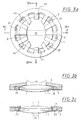
- Figure 1 shows a lens frame 2, in which a lens 1 by a plurality of webs 21-28 (eight are shown) is kept largely tension-free and exactly fixed in position.
- the webs 21-28 spoke, tabs
- the webs 21-28 are glued to the edge of the lens 1 or connected by other joining methods.
- the lens 1 is illuminated.
- the problem is that the lens materials have considerable absorption and consequently in cross section 10 takes place a considerable heat.
- the associated increase in temperature causes a change in the refractive index and by the thermal expansion in addition to a deformation. Overall, there is a change in the lens effect with astigmatic effect.
- the cooling takes place only to a small extent via the ambient gas (in the case of projection exposure systems, as a rule, helium) and by heat radiation.
- the primary heat is the heat over the lens body 1, the joint (gluing) and the gas in the Environment of the joint and the webs 21-28 discharged to the socket 2.
- the webs 21-28 in this example are made of different materials, with which they have different thermal conductivity.
- the webs 21, 25 closest to the slit-shaped cross-section 10 are of very good thermal conductivity, the most distant lead 23, 27 of low thermal conductivity lead, and the intermediate webs 22, 24, 26, 28 of medium thermal conductivity aluminum.
- the temperature distribution in the lens 1 is thus relatively lowered between the webs 21, 23 and relatively raised between the webs 23, 27, resulting in a - at least partially - homogenization and symmetrization of the temperature distribution and a reduced disturbance of the optical properties of the lens 1.
- lens 1 and socket 2 are connected via webs 211 to 214 (four pieces only for clear presentation, in practice more) with different cross section and thus different heat conduction. Different mechanical properties are prevented by each web 211 to 214 having similar spring joints 221 to 224. The heat conduction through the adjoining narrow gaps (only minimal mobility of the joints are required) takes place sufficiently effectively by the filling gas (helium) or by a flexible metal cable (stranded wire) connected in parallel (see FIG. 6b).
- FIG. 2 Also shown in this Figure 2 is a "dipole" illumination of the lens with two eccentric spots 101, 102 as seen in the area of the aperture plane and equivalent planes of symmetrical slant illumination projection exposure systems. Also, this results in astigmatic errors due to the absorption of light, which can be reduced by the passive compensating cooling.
- Figure 3a-c shows a variant of the invention with an additional, provided only for the compensatory cooling, heat-conducting element 3rd
- Lens 1 and 2 socket are connected, for example, with uniform webs or with selectively cooling webs 21-28 of Figure 1 or 2. Any other socket technique is equally applicable.
- the heat-conducting element 3 is firmly connected to the socket 2 with good thermal conductivity and covers parts of the lens 1, which are not penetrated by the light, that is outside of the illuminated area 10 shown here as a slot.
- This overlap preferably occurs without contact, for example at a distance of about 0.1 mm, so that a good heat transfer is ensured by the intermediary of the filling gas, but at the same time no stresses can be introduced into the lens 1.
- Better heat conduction results, of course, when the gap between the lens 1 and thermally conductive element 3 with adhesive, a gel, liquid crystals or the like, as little as possible voltage-transmitting material is filled.
- the heat-conducting element 3 With the embodiment of the heat-conducting element 3 with a plurality of fingers or spokes shown in FIG. 3a, its width, shape and distribution can also be used to adjust the heat conduction. Even when designed as a continuous disc or pinhole, the thickness of the heat-conducting element can be made locally different. It is also possible to make the individual fingers analogous to the webs 21-28 of Figure 1 from different heat-conducting materials. Of course, the heat-conducting element 3 can also be arranged on both sides of the lens 1.
- FIG. 4 shows in a representation corresponding to FIG. 3b a possibility of how the cooling element 3 can be brought into material or positive contact with the lens 1 without the mechanical properties of the socket 2 and the connecting parts 21 being disturbed.
- the cooling element 3 is for this purpose equipped with a flexible thermally conductive cable 30 - e.g. a copper wire - and connected to a heat sink 20.
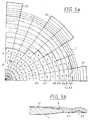
- Figure 5a shows in plan view the finite element model of a quadrant of a lens 1 made of quartz glass (center thickness 14.4 mm, upper radius of curvature 1600 mm, lower radius of curvature 220 mm - biconvex -, diameter 160 mm).
- Eight massive tabs (51, 52, 53) made of aluminum are evenly distributed on the lens 1 in the manner visible from the section 5b. They are 30 mm wide, 2 mm thick above the lens and 6 mm radially overlapping, outside they are again radially 8 mm long in 4 mm thickness. At the outer edge, they are kept at base temperature, e.g. by flexible thermally conductive strands 50.
- cooling straps located on the Y-axis are omitted.
- the lying on the X-axis cooling flaps 510 are doubled in width and also made of the better heat-conducting silver.
- the tabs 52 between them remain unchanged, as well as the heat in the area 4.
- the temperature increase at the center is now 9.2 milligrams.
- the isotherms are now well rotationally symmetric up to about 0.7 times the maximum temperature increase and half the lens diameter.
- the mechanical version of the lens 1 can either be done by the cooling straps 510, 52, or it is provided any socket technology, which preferably has comparatively low heat conduction.
- Figure 7 shows a variant similar to Figure 3a-c, in which the fingers 31, 32 of the thermally conductive element made of bimetal - two layers of material with different thermal expansion - are executed.
- the bimetallic strip 31 On the left in the picture, the bimetallic strip 31 is bent away from the lens 1 at the low temperature t 1 , it can absorb only a small amount of heat.
- the bimetallic strip 32 is stretched and is located at a small distance from the lens 1, so that it can dissipate a lot of heat.
- the invention can also be applied to prismatic parts, to gratings or mirrors, even to all non-uniformly heat-stressed optical components.
- FIG. 8 shows an embodiment specially adapted to a mirror 6.
- the mirror 6 is supported on a holder 7 via supports 71 to 77 distributed on its rear side - individual webs or support rings.
- the different thermal expansion of the materials for the supports 71-77 can also be specifically exploited to compensate for Deformationen.des mirror 6 due to heating, or also bring about targeted. In the latter case, disturbances of other optical elements that interact with the mirror 6 in a system can then be compensated.
- FIG 9 shows the complete optical system of a projection exposure system of microlithography in a schematic overview.
- a DUV excimer laser serves as the light source 61.
- a beam-shaping optics 62 with a zoom axicon objective 63, optionally a diaphragm 64 (exchangeable, conventional, annular aperture, dipole, quadrupole aperture) and a homogenizing quartz rod 65 illuminate the REMA.
- Aperture 66 homogeneous, which is mapped by the following REMA lens 67 as sharply bordered homogeneous spot, especially as a narrow scan slot on the mask 68.
- the following reducing projection lens 69 images the mask 68 on the wafer 70.
- the near-field lenses 671 and 672 of the REMA objective 67 and 692 of the projection lens 69 are now preferred optical elements on which the cooling according to the invention is used. This cooling reduces the aberrations that occur in a scanner in which mask 68 and wafer 70 are synchronously scanned due to the narrow slit-shaped illuminated field.
- the lens 691 is disposed next to the aperture 690 of the projection lens 69. It is controlled by special types of lighting, e.g. Dipole aperture, particularly stressed (see Figure 2). By asymmetric cooling according to the invention, however, this disorder can also be reduced.
Landscapes
- Physics & Mathematics (AREA)
- General Physics & Mathematics (AREA)
- Health & Medical Sciences (AREA)
- Engineering & Computer Science (AREA)
- Environmental & Geological Engineering (AREA)
- Epidemiology (AREA)
- Public Health (AREA)
- Life Sciences & Earth Sciences (AREA)
- Atmospheric Sciences (AREA)
- Toxicology (AREA)
- Optics & Photonics (AREA)
- Exposure And Positioning Against Photoresist Photosensitive Materials (AREA)
- Exposure Of Semiconductors, Excluding Electron Or Ion Beam Exposure (AREA)
Applications Claiming Priority (3)
| Application Number | Priority Date | Filing Date | Title |
|---|---|---|---|
| DE19807094A DE19807094A1 (de) | 1998-02-20 | 1998-02-20 | Optische Anordnung und Projektionsbelichtungsanlage der Mikrolithographie mit passiver thermischer Kompensation |
| DE19807094 | 1998-02-20 | ||
| EP99100845A EP0938009B1 (de) | 1998-02-20 | 1999-01-19 | Optische Anordnung und Projektionsbelichtungsanlage der Mikrolithographie mit passiver thermischer Kompensation |
Related Parent Applications (1)
| Application Number | Title | Priority Date | Filing Date |
|---|---|---|---|
| EP99100845A Division EP0938009B1 (de) | 1998-02-20 | 1999-01-19 | Optische Anordnung und Projektionsbelichtungsanlage der Mikrolithographie mit passiver thermischer Kompensation |
Publications (2)
| Publication Number | Publication Date |
|---|---|
| EP1596235A1 EP1596235A1 (de) | 2005-11-16 |
| EP1596235B1 true EP1596235B1 (de) | 2007-02-28 |
Family
ID=7858359
Family Applications (2)
| Application Number | Title | Priority Date | Filing Date |
|---|---|---|---|
| EP05106797A Expired - Lifetime EP1596235B1 (de) | 1998-02-20 | 1999-01-19 | Projektionsbelichtungsanlage der Mikrolithographie mit passiver thermischer Kompensation |
| EP99100845A Expired - Lifetime EP0938009B1 (de) | 1998-02-20 | 1999-01-19 | Optische Anordnung und Projektionsbelichtungsanlage der Mikrolithographie mit passiver thermischer Kompensation |
Family Applications After (1)
| Application Number | Title | Priority Date | Filing Date |
|---|---|---|---|
| EP99100845A Expired - Lifetime EP0938009B1 (de) | 1998-02-20 | 1999-01-19 | Optische Anordnung und Projektionsbelichtungsanlage der Mikrolithographie mit passiver thermischer Kompensation |
Country Status (5)
| Country | Link |
|---|---|
| EP (2) | EP1596235B1 (https=) |
| JP (1) | JPH11287936A (https=) |
| KR (1) | KR100593429B1 (https=) |
| DE (3) | DE19807094A1 (https=) |
| TW (1) | TW401516B (https=) |
Families Citing this family (24)
| Publication number | Priority date | Publication date | Assignee | Title |
|---|---|---|---|---|
| US7274430B2 (en) | 1998-02-20 | 2007-09-25 | Carl Zeiss Smt Ag | Optical arrangement and projection exposure system for microlithography with passive thermal compensation |
| DE19956353C1 (de) * | 1999-11-24 | 2001-08-09 | Zeiss Carl | Optische Anordnung |
| DE19959741A1 (de) * | 1999-12-10 | 2001-06-13 | Zeiss Carl | Vorrichtung zur deformationsarmen Lagerung eines optischen Elementes und Verfahren zur deformationsarmen Lagerung des optischen Elementes |
| DE19963588C2 (de) | 1999-12-29 | 2002-01-10 | Zeiss Carl | Optische Anordnung |
| US6621557B2 (en) | 2000-01-13 | 2003-09-16 | Nikon Corporation | Projection exposure apparatus and exposure methods |
| DE10151919B4 (de) * | 2001-10-20 | 2007-02-01 | Carl Zeiss Smt Ag | Belichtungsobjektiv in der Halbleiterlithographie |
| EP1310829B1 (en) * | 2001-11-07 | 2007-05-02 | ASML Netherlands B.V. | Lithographic apparatus and device manufacturing method |
| JP2003218023A (ja) * | 2002-01-28 | 2003-07-31 | Nikon Corp | X線反射鏡、x線露光転写装置及び半導体デバイスの製造方法 |
| DE10210893A1 (de) * | 2002-03-07 | 2003-09-18 | Zeiss Carl Laser Optics Gmbh | Optische Anordnung mit einem optischen Bauelement, insbesondere einer Blende |
| JP4590205B2 (ja) * | 2003-05-14 | 2010-12-01 | キヤノン株式会社 | ミラー保持方法、光学装置、露光装置、およびデバイス製造方法 |
| GB0511692D0 (en) | 2005-06-08 | 2005-07-13 | Digital Projection Ltd | Heat transfer apparatus |
| DE102006021797A1 (de) * | 2006-05-09 | 2007-11-15 | Carl Zeiss Smt Ag | Optische Abbildungseinrichtung mit thermischer Dämpfung |
| GB2451684A (en) | 2007-08-09 | 2009-02-11 | Digital Projection Ltd | Heat transfer apparatus for cooling a light valve or digital micro mirror |
| WO2009124590A1 (en) * | 2008-04-09 | 2009-10-15 | Carl Zeiss Smt Ag | Optical aperture device |
| DE102009035788B4 (de) * | 2009-07-31 | 2011-06-30 | Carl Zeiss Laser Optics GmbH, 73447 | Optische Anordnung in einem optischen System, insbesondere einer Beleuchtungseinrichtung |
| DE102013203032A1 (de) * | 2013-02-25 | 2014-02-27 | Carl Zeiss Smt Gmbh | Optische Anordnung mit einem optischen Element und einem zusätzlichen Wärmeleitelement |
| CN103499865B (zh) * | 2013-10-10 | 2015-07-29 | 中国科学院上海技术物理研究所 | 一种具有热应力缓冲结构的滤光片安装支架 |
| DE102015115931B3 (de) * | 2015-09-21 | 2016-10-27 | Jenoptik Optical Systems Gmbh | Spannungsentkoppelte monolithische Linsenfassung |
| DE102015115929B3 (de) | 2015-09-21 | 2016-10-06 | Jenoptik Optical Systems Gmbh | Monolithische Linsenfassung |
| DE102017217111A1 (de) * | 2017-09-26 | 2019-03-28 | Robert Bosch Gmbh | Anordnung eines optischen Systems und Entwärmungsverfahren |
| DE102017217107A1 (de) * | 2017-09-26 | 2019-03-28 | Robert Bosch Gmbh | Anordnung eines optischen Systems und Entwärmungsverfahren |
| JP7061666B2 (ja) * | 2017-10-30 | 2022-04-28 | エーエスエムエル ホールディング エヌ.ブイ. | 半導体フォトリソグラフィで使用するためのアセンブリ及び同一のものを製造する方法 |
| JP6951498B2 (ja) * | 2019-06-25 | 2021-10-20 | キヤノン株式会社 | 露光装置、露光方法および物品製造方法 |
| IL284361B2 (en) * | 2021-06-24 | 2024-08-01 | Rafael Advanced Defense Systems Ltd | Temperature balanced spacer |
Family Cites Families (11)
| Publication number | Priority date | Publication date | Assignee | Title |
|---|---|---|---|---|
| US4057332A (en) * | 1976-04-21 | 1977-11-08 | Caterpillar Tractor Co. | Peripherally cooled laser lens assembly |
| US4155631A (en) * | 1977-04-14 | 1979-05-22 | W. J. Schafer Associates, Inc. | Apparatus for compensating for thermally introduced distortions in reflecting surfaces |
| JPS56102392A (en) * | 1980-01-22 | 1981-08-15 | Nec Corp | Laser working optical device |
| JPS6037632B2 (ja) * | 1983-02-15 | 1985-08-27 | 株式会社東芝 | 固体レ−ザ発振装置 |
| JPS59175178A (ja) * | 1983-03-24 | 1984-10-03 | Mitsubishi Electric Corp | レ−ザ装置 |
| JPS61208002A (ja) * | 1985-03-13 | 1986-09-16 | Toshiba Corp | 光透過装置 |
| DE69220868T2 (de) | 1991-09-07 | 1997-11-06 | Canon K.K., Tokio/Tokyo | System zur Stabilisierung der Formen von optischen Elementen, Belichtungsvorrichtung unter Verwendung dieses Systems und Verfahren zur Herstellung von Halbleitervorrichtungen |
| JPH05203884A (ja) * | 1992-01-24 | 1993-08-13 | Toshiba Corp | 光学素子 |
| JP3169267B2 (ja) * | 1992-06-17 | 2001-05-21 | パイオニア株式会社 | 液体プリズム |
| JP3368091B2 (ja) * | 1994-04-22 | 2003-01-20 | キヤノン株式会社 | 投影露光装置及びデバイスの製造方法 |
| US5881088A (en) * | 1997-01-08 | 1999-03-09 | Trw Inc. | Face-cooled high-power laser optic cell |
-
1998
- 1998-02-20 DE DE19807094A patent/DE19807094A1/de not_active Withdrawn
- 1998-12-22 KR KR1019980057360A patent/KR100593429B1/ko not_active Expired - Fee Related
-
1999
- 1999-01-11 TW TW088100316A patent/TW401516B/zh not_active IP Right Cessation
- 1999-01-19 DE DE59912313T patent/DE59912313D1/de not_active Expired - Fee Related
- 1999-01-19 EP EP05106797A patent/EP1596235B1/de not_active Expired - Lifetime
- 1999-01-19 EP EP99100845A patent/EP0938009B1/de not_active Expired - Lifetime
- 1999-01-19 DE DE59914228T patent/DE59914228D1/de not_active Expired - Fee Related
- 1999-02-15 JP JP11035932A patent/JPH11287936A/ja active Pending
Also Published As
| Publication number | Publication date |
|---|---|
| DE59914228D1 (de) | 2007-04-12 |
| KR19990071443A (ko) | 1999-09-27 |
| DE19807094A1 (de) | 1999-08-26 |
| EP0938009A1 (de) | 1999-08-25 |
| KR100593429B1 (ko) | 2006-10-24 |
| EP0938009B1 (de) | 2005-07-27 |
| JPH11287936A (ja) | 1999-10-19 |
| TW401516B (en) | 2000-08-11 |
| EP1596235A1 (de) | 2005-11-16 |
| DE59912313D1 (de) | 2005-09-01 |
Similar Documents
| Publication | Publication Date | Title |
|---|---|---|
| EP1596235B1 (de) | Projektionsbelichtungsanlage der Mikrolithographie mit passiver thermischer Kompensation | |
| DE19963588C2 (de) | Optische Anordnung | |
| DE10000191B4 (de) | Projektbelichtungsanlage der Mikrolithographie | |
| DE19963587B4 (de) | Projektions-Belichtungsanlage | |
| EP0783137B1 (de) | REMA-Objektiv für Mikrolithographie-Projektionsbelichtungsanlagen | |
| DE19956353C1 (de) | Optische Anordnung | |
| DE60210010T2 (de) | Kollimationssystem für Laserdiode | |
| DE102009029776B3 (de) | Optisches Element | |
| US20080212052A1 (en) | Optical arrangement and projection exposure system for microlithography with passive thermal compensation | |
| DE102006034755A1 (de) | Optische Vorrichtung sowie Verfahren zur Korrektur bzw. Verbesserung des Abbildungsverhaltens einer optischen Vorrichtung | |
| DE19757074A1 (de) | Projektionsbelichtungsanlage und Belichtungsverfahren | |
| EP2100190A1 (de) | Beleuchtungsoptik und projektionsbelichtungsanlage für die mikrolithographie | |
| DE10140208A1 (de) | Optische Anordnung | |
| DE102012223034A1 (de) | Beleuchtungssystem einer Mikrolithographischen Projektionsbelichtungsanlage | |
| DE102009033818A1 (de) | Temperiervorrichtung für eine optische Baugruppe | |
| WO1997025722A2 (de) | Kondensor-monochromator-anordnung für röntgenstrahlung | |
| DE102007039019A1 (de) | Vorrichtung zum Schwenken eines optischen Strahls | |
| DE102004014766A1 (de) | Verfahren zur Verzeichnungskorrektur in einer mikrolithographischen Projektionsbelichtungsanlage | |
| DE10045265A1 (de) | Vorrichtung zum Bündeln der Strahlung einer Lichtquelle | |
| WO2021160583A1 (de) | Projektionsbelichtungsanlage mit einem thermischen manipulator | |
| DE102007061194A1 (de) | Beleuchtungssystem für die EUV-Mikro-Lithografie, Projektionsbelichtungsanlage für die EUV-Mikro-Lithografie, Verfahren zur Korrektur der Elliptizität und/oder der Uniformität innerhalb einer derartigen Projektionsbelichtungsanlage, Verfahren zur Herstellung eines mikrostrukturierten Bauteils sowie mit dem Herstellungsverfahren hergestelltes Bauteil | |
| EP1182507A2 (de) | Projektionsbelichtungsanlage | |
| DE10132988B4 (de) | Projektionsbelichtungsanlage | |
| WO2021089579A1 (de) | Projektionsbelichtungsanlage für die halbleiterlithographie | |
| DE102008000968A1 (de) | Optisches Korrekturelement und Verfahren zur Korrektur von temperaturinduzierten Abbildungsfehlern in optischen Systemen, Projektionsobjektiv und Projektionsbelichtungsanlage für die Halbleiterlithographie |
Legal Events
| Date | Code | Title | Description |
|---|---|---|---|
| PUAI | Public reference made under article 153(3) epc to a published international application that has entered the european phase |
Free format text: ORIGINAL CODE: 0009012 |
|
| AC | Divisional application: reference to earlier application |
Ref document number: 0938009 Country of ref document: EP Kind code of ref document: P |
|
| AK | Designated contracting states |
Kind code of ref document: A1 Designated state(s): DE FR GB IE IT NL |
|
| AX | Request for extension of the european patent |
Extension state: AL BA HR MK YU |
|
| AKX | Designation fees paid | ||
| 17P | Request for examination filed |
Effective date: 20060706 |
|
| RBV | Designated contracting states (corrected) |
Designated state(s): DE FR IT NL |
|
| GRAP | Despatch of communication of intention to grant a patent |
Free format text: ORIGINAL CODE: EPIDOSNIGR1 |
|
| GRAS | Grant fee paid |
Free format text: ORIGINAL CODE: EPIDOSNIGR3 |
|
| GRAA | (expected) grant |
Free format text: ORIGINAL CODE: 0009210 |
|
| RAP1 | Party data changed (applicant data changed or rights of an application transferred) |
Owner name: CARL ZEISS SMT AG |
|
| AC | Divisional application: reference to earlier application |
Ref document number: 0938009 Country of ref document: EP Kind code of ref document: P |
|
| AK | Designated contracting states |
Kind code of ref document: B1 Designated state(s): DE FR IT NL |
|
| REF | Corresponds to: |
Ref document number: 59914228 Country of ref document: DE Date of ref document: 20070412 Kind code of ref document: P |
|
| EN | Fr: translation not filed | ||
| PLBE | No opposition filed within time limit |
Free format text: ORIGINAL CODE: 0009261 |
|
| STAA | Information on the status of an ep patent application or granted ep patent |
Free format text: STATUS: NO OPPOSITION FILED WITHIN TIME LIMIT |
|
| 26N | No opposition filed |
Effective date: 20071129 |
|
| PG25 | Lapsed in a contracting state [announced via postgrant information from national office to epo] |
Ref country code: FR Free format text: LAPSE BECAUSE OF FAILURE TO SUBMIT A TRANSLATION OF THE DESCRIPTION OR TO PAY THE FEE WITHIN THE PRESCRIBED TIME-LIMIT Effective date: 20071019 |
|
| PG25 | Lapsed in a contracting state [announced via postgrant information from national office to epo] |
Ref country code: FR Free format text: LAPSE BECAUSE OF FAILURE TO SUBMIT A TRANSLATION OF THE DESCRIPTION OR TO PAY THE FEE WITHIN THE PRESCRIBED TIME-LIMIT Effective date: 20070228 |
|
| PGFP | Annual fee paid to national office [announced via postgrant information from national office to epo] |
Ref country code: DE Payment date: 20090122 Year of fee payment: 11 |
|
| PG25 | Lapsed in a contracting state [announced via postgrant information from national office to epo] |
Ref country code: DE Free format text: LAPSE BECAUSE OF NON-PAYMENT OF DUE FEES Effective date: 20100803 |
|
| PGFP | Annual fee paid to national office [announced via postgrant information from national office to epo] |
Ref country code: NL Payment date: 20150129 Year of fee payment: 17 |
|
| PGFP | Annual fee paid to national office [announced via postgrant information from national office to epo] |
Ref country code: IT Payment date: 20150126 Year of fee payment: 17 |
|
| REG | Reference to a national code |
Ref country code: NL Ref legal event code: MM Effective date: 20160201 |
|
| PG25 | Lapsed in a contracting state [announced via postgrant information from national office to epo] |
Ref country code: NL Free format text: LAPSE BECAUSE OF NON-PAYMENT OF DUE FEES Effective date: 20160201 |
|
| PG25 | Lapsed in a contracting state [announced via postgrant information from national office to epo] |
Ref country code: IT Free format text: LAPSE BECAUSE OF NON-PAYMENT OF DUE FEES Effective date: 20160119 |