EP1593161B1 - Strained channel finfet - Google Patents
Strained channel finfet Download PDFInfo
- Publication number
- EP1593161B1 EP1593161B1 EP04702513.5A EP04702513A EP1593161B1 EP 1593161 B1 EP1593161 B1 EP 1593161B1 EP 04702513 A EP04702513 A EP 04702513A EP 1593161 B1 EP1593161 B1 EP 1593161B1
- Authority
- EP
- European Patent Office
- Prior art keywords
- fin
- layer
- crystalline material
- channel layer
- strained channel
- Prior art date
- Legal status (The legal status is an assumption and is not a legal conclusion. Google has not performed a legal analysis and makes no representation as to the accuracy of the status listed.)
- Expired - Lifetime
Links
- 239000002178 crystalline material Substances 0.000 claims description 44
- 238000000034 method Methods 0.000 claims description 20
- 230000005669 field effect Effects 0.000 claims description 9
- 229910052710 silicon Inorganic materials 0.000 claims description 9
- 239000010703 silicon Substances 0.000 claims description 9
- 229910021420 polycrystalline silicon Inorganic materials 0.000 claims description 5
- 229920005591 polysilicon Polymers 0.000 claims description 5
- 239000000969 carrier Substances 0.000 claims 3
- 230000008569 process Effects 0.000 description 9
- 239000012212 insulator Substances 0.000 description 8
- 239000000758 substrate Substances 0.000 description 8
- XUIMIQQOPSSXEZ-UHFFFAOYSA-N Silicon Chemical compound [Si] XUIMIQQOPSSXEZ-UHFFFAOYSA-N 0.000 description 7
- 230000015572 biosynthetic process Effects 0.000 description 4
- 238000000151 deposition Methods 0.000 description 3
- 238000005530 etching Methods 0.000 description 3
- 239000000463 material Substances 0.000 description 3
- VYPSYNLAJGMNEJ-UHFFFAOYSA-N Silicium dioxide Chemical compound O=[Si]=O VYPSYNLAJGMNEJ-UHFFFAOYSA-N 0.000 description 2
- 229910000577 Silicon-germanium Inorganic materials 0.000 description 2
- BOTDANWDWHJENH-UHFFFAOYSA-N Tetraethyl orthosilicate Chemical compound CCO[Si](OCC)(OCC)OCC BOTDANWDWHJENH-UHFFFAOYSA-N 0.000 description 2
- MCMNRKCIXSYSNV-UHFFFAOYSA-N Zirconium dioxide Chemical compound O=[Zr]=O MCMNRKCIXSYSNV-UHFFFAOYSA-N 0.000 description 2
- 230000008021 deposition Effects 0.000 description 2
- 239000003989 dielectric material Substances 0.000 description 2
- 239000011810 insulating material Substances 0.000 description 2
- 238000012986 modification Methods 0.000 description 2
- 230000004048 modification Effects 0.000 description 2
- 101100269850 Caenorhabditis elegans mask-1 gene Proteins 0.000 description 1
- 229910004541 SiN Inorganic materials 0.000 description 1
- PNEYBMLMFCGWSK-UHFFFAOYSA-N aluminium oxide Inorganic materials [O-2].[O-2].[O-2].[Al+3].[Al+3] PNEYBMLMFCGWSK-UHFFFAOYSA-N 0.000 description 1
- 229910052681 coesite Inorganic materials 0.000 description 1
- 229910052593 corundum Inorganic materials 0.000 description 1
- 229910052906 cristobalite Inorganic materials 0.000 description 1
- 238000005137 deposition process Methods 0.000 description 1
- 230000000694 effects Effects 0.000 description 1
- 229910052732 germanium Inorganic materials 0.000 description 1
- GNPVGFCGXDBREM-UHFFFAOYSA-N germanium atom Chemical compound [Ge] GNPVGFCGXDBREM-UHFFFAOYSA-N 0.000 description 1
- 230000006698 induction Effects 0.000 description 1
- 229910001635 magnesium fluoride Inorganic materials 0.000 description 1
- 238000004519 manufacturing process Methods 0.000 description 1
- 150000004767 nitrides Chemical class 0.000 description 1
- 238000012856 packing Methods 0.000 description 1
- 238000000059 patterning Methods 0.000 description 1
- 238000005498 polishing Methods 0.000 description 1
- 230000009467 reduction Effects 0.000 description 1
- 239000004065 semiconductor Substances 0.000 description 1
- 239000000377 silicon dioxide Substances 0.000 description 1
- LIVNPJMFVYWSIS-UHFFFAOYSA-N silicon monoxide Inorganic materials [Si-]#[O+] LIVNPJMFVYWSIS-UHFFFAOYSA-N 0.000 description 1
- 229910052814 silicon oxide Inorganic materials 0.000 description 1
- 229910052682 stishovite Inorganic materials 0.000 description 1
- -1 structures Substances 0.000 description 1
- 239000000126 substance Substances 0.000 description 1
- 229910052905 tridymite Inorganic materials 0.000 description 1
- 229910001845 yogo sapphire Inorganic materials 0.000 description 1
Images


Classifications
-
- H—ELECTRICITY
- H10—SEMICONDUCTOR DEVICES; ELECTRIC SOLID-STATE DEVICES NOT OTHERWISE PROVIDED FOR
- H10D—INORGANIC ELECTRIC SEMICONDUCTOR DEVICES
- H10D30/00—Field-effect transistors [FET]
- H10D30/60—Insulated-gate field-effect transistors [IGFET]
- H10D30/62—Fin field-effect transistors [FinFET]
-
- H—ELECTRICITY
- H10—SEMICONDUCTOR DEVICES; ELECTRIC SOLID-STATE DEVICES NOT OTHERWISE PROVIDED FOR
- H10D—INORGANIC ELECTRIC SEMICONDUCTOR DEVICES
- H10D30/00—Field-effect transistors [FET]
- H10D30/01—Manufacture or treatment
- H10D30/021—Manufacture or treatment of FETs having insulated gates [IGFET]
- H10D30/024—Manufacture or treatment of FETs having insulated gates [IGFET] of fin field-effect transistors [FinFET]
-
- H—ELECTRICITY
- H10—SEMICONDUCTOR DEVICES; ELECTRIC SOLID-STATE DEVICES NOT OTHERWISE PROVIDED FOR
- H10D—INORGANIC ELECTRIC SEMICONDUCTOR DEVICES
- H10D30/00—Field-effect transistors [FET]
- H10D30/60—Insulated-gate field-effect transistors [IGFET]
- H10D30/67—Thin-film transistors [TFT]
- H10D30/6729—Thin-film transistors [TFT] characterised by the electrodes
- H10D30/6737—Thin-film transistors [TFT] characterised by the electrodes characterised by the electrode materials
- H10D30/6739—Conductor-insulator-semiconductor electrodes
-
- H—ELECTRICITY
- H10—SEMICONDUCTOR DEVICES; ELECTRIC SOLID-STATE DEVICES NOT OTHERWISE PROVIDED FOR
- H10D—INORGANIC ELECTRIC SEMICONDUCTOR DEVICES
- H10D30/00—Field-effect transistors [FET]
- H10D30/60—Insulated-gate field-effect transistors [IGFET]
- H10D30/67—Thin-film transistors [TFT]
- H10D30/674—Thin-film transistors [TFT] characterised by the active materials
- H10D30/6741—Group IV materials, e.g. germanium or silicon carbide
- H10D30/6743—Silicon
- H10D30/6744—Monocrystalline silicon
-
- H—ELECTRICITY
- H10—SEMICONDUCTOR DEVICES; ELECTRIC SOLID-STATE DEVICES NOT OTHERWISE PROVIDED FOR
- H10D—INORGANIC ELECTRIC SEMICONDUCTOR DEVICES
- H10D30/00—Field-effect transistors [FET]
- H10D30/60—Insulated-gate field-effect transistors [IGFET]
- H10D30/67—Thin-film transistors [TFT]
- H10D30/674—Thin-film transistors [TFT] characterised by the active materials
- H10D30/6741—Group IV materials, e.g. germanium or silicon carbide
- H10D30/6748—Group IV materials, e.g. germanium or silicon carbide having a multilayer structure or superlattice structure
-
- H—ELECTRICITY
- H10—SEMICONDUCTOR DEVICES; ELECTRIC SOLID-STATE DEVICES NOT OTHERWISE PROVIDED FOR
- H10D—INORGANIC ELECTRIC SEMICONDUCTOR DEVICES
- H10D30/00—Field-effect transistors [FET]
- H10D30/60—Insulated-gate field-effect transistors [IGFET]
- H10D30/751—Insulated-gate field-effect transistors [IGFET] having composition variations in the channel regions
-
- H—ELECTRICITY
- H10—SEMICONDUCTOR DEVICES; ELECTRIC SOLID-STATE DEVICES NOT OTHERWISE PROVIDED FOR
- H10D—INORGANIC ELECTRIC SEMICONDUCTOR DEVICES
- H10D30/00—Field-effect transistors [FET]
- H10D30/60—Insulated-gate field-effect transistors [IGFET]
- H10D30/791—Arrangements for exerting mechanical stress on the crystal lattice of the channel regions
Definitions
- the present invention relates generally to transistors and, more particularly, to fin field effect transistors (FinFETs).
- FinFETs fin field effect transistors
- Scaling of device dimensions has been a primary factor driving improvements in integrated circuit performance and reduction in integrated circuit cost. Due to limitations associated with existing gate-oxide thicknesses and source/drain (S/D) junction depths, scaling of existing bulk MOSFET devices below the 0.1 ⁇ m process generation may be difficult, if not impossible. New device structures and new materials, thus, are likely to be needed to improve FET performance.
- Double-gate MOSFETs represent new devices that are candidates for succeeding existing planar MOSFETs.
- double-gate MOSFETs the use of two gates to control the channel significantly suppresses short-channel effects.
- a FinFET is a recent double-gate structure that includes a channel formed in a vertical fin.
- the FinFET is similar to existing planar MOSFET in layout and fabrication.
- the FinFET also provides a range of channel lengths, CMOS compatibility and large packing density compared to other double-gate structures.
- a FinFET transistor uses a vertically formed strained channel layer that is self-aligned to the fin channel.
- the strained channel layer includes a crystalline material that is lattice constant mismatched with the crystalline material of the fin of the FinFET.
- the lattice constant mismatch induces tensile strain within the strained channel layer that increases carrier mobility. Increasing the carrier mobility, in turn, increases the drive current of the FinFET transistor, thus, improving FinFET performance.
- a field effect transistor that includes a fin.
- the fin includes a first crystalline material and a plurality of surfaces.
- the structure further includes a layer formed on at least a portion of the plurality of surfaces, the layer including a second crystalline material.
- the first crystalline material has a different lattice constant than the second crystalline material to induce tensile strain within the layer.
- a transistor includes a fin that further includes a first crystalline material and first and second end portions.
- the first crystalline material has a first lattice constant.
- the transistor further includes source and drain regions formed adjacent the first and second end portions of the fin.
- the transistor also includes a first layer of second crystalline material formed on at least a portion of the fin.
- the second crystalline material has a second lattice constant, wherein the first lattice constant is greater than the second lattice constant.
- the transistor additionally includes a dielectric layer formed on at least a portion of the first layer and a gate electrode formed on at least a portion of the dielectric layer.
- a method of forming a fin field effect transistor includes forming a fin that includes a first crystalline material and multiple surfaces. The method further includes forming a first layer on at least a portion of the multiple surfaces. The first layer includes a second crystalline material, wherein the first crystalline material is lattice constant mismatched with the second crystalline material to induce tensile strain within the first layer.
- an increased mobility channel FinFET is provided.
- a vertically formed strained channel layer consistent with the present invention, is self-aligned to the fin channel of the FinFET.
- the strained channel layer includes a crystalline material that is lattice mismatched with the crystalline material of the fin of the FinFET such that tensile strain is induced within the strained channel layer.
- the induced tensile strain increases carrier mobility of the strained channel layer, thus, increasing drive current of the FinFET.
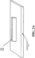
- FIG. 1 illustrates a cross-section of a substrate 100 formed in accordance with an exemplary embodiment of the present invention.
- Substrate 100 may be a silicon on insulator (SOI) structure that includes a fin channel layer 105 formed upon, for example, a buried oxide layer 110. Buried oxide layer 110 may be formed on a silicon layer (not shown).
- the thickness of fin channel layer 105 may range, for example, from about 500 ⁇ to about 2000 ⁇ and the thickness of buried oxide layer 110 may range, for example, from about 1000 ⁇ to about 3000 ⁇ .
- Fin channel layer 105 includes a crystalline material with a lattice constant larger than the lattice constant of a crystalline material selected for a strained channel layer (described with respect to FIGS. 3A and 3B below). If, for example, silicon is selected for the strained channel layer, fin channel layer 105 may include a crystalline material with a lattice constant large than the lattice constant of silicon. Fin channel layer 105 may include, for example, Si x Ge (1-x) with x approximately equal to 0.7. Other values of x may be appropriately selected.
- substrate 100 may be formed by wafer bonding epitaxial Si x Ge (1-x) to an oxide/Si substrate wafer.
- substrate 100 may be formed by wafer bonding epitaxial Si x Ge (1-x) to an oxide/Si substrate wafer.
- a vertical fin 205 may be formed from fin channel layer 105.
- Fin 205 is formed with a width (w) in a range of 10-15 nm.
- Fin 205 may be formed from fin channel layer 105 using any existing process, including, but not limited to, existing photolithographic and etching processes.
- Source 210 and drain 215 regions may be formed adjacent the respective ends of fin 205, as shown in FIGS. 2C and 2D .
- Source 210 and drain 215 regions may be formed by, for example, deposition of a layer of crystalline material over fin 205.
- the source 210 and drain 215 regions may be formed from the layer of crystalline material using, for example, existing photolithographic and etching processes.
- Source 210 and drain 215 regions may include a crystalline material such as, for example, Si x Ge (1-x) , with x approximately equal to 0.7.
- a strained layer 305 is formed on fin 205, source 210 and drain 215, as shown in FIGS. 3A and 3B .
- Strained layer 305 may be formed on fin 205, source 210 and drain 215 using any appropriate existing process.
- strained layer 305 may be formed on fin 205, source 210 and drain 215 using a selective epitaxial deposition process.
- Strained layer 305 includes a crystalline material whose lattice constant is smaller that the lattice constant of the crystalline material used for fin 205. With a lattice mismatch between fin 205 and strained layer 305 tensile strain is produced in strained layer 305.
- Strained layer 305 may be formed, for example, with a thickness t that is approximately 1/2 to 1/3 of the fin 205 width w.
- the thickness t of strained layer 305 may be 5 nm.
- Strained layer 305 comprises silicon.
- other crystalline materials with lattice constants less than the crystalline material used to form fin 205 may, alternatively, be used.
- a gate dielectric 405 and gate electrode 410 may be formed on the portion of fin 205 not covered by source 210 and drain 215, as shown in FIGS. 4A and 4B .
- the gate dielectric 405 may include a thin layer of dielectric material, such as SiO, SiO 2 , SiN, SiON, HFO 2 , ZrO 2 , Al 2 O 3 , HFSiO(x) ZnS, MgF 2 , or other dielectric materials.
- Gate electrode 410 may be formed upon gate dielectric 405 and may include, for example, a layer of polysilicon. Gate dielectric 405 and gate electrode 410 may be formed on fin 205 using any existing processes, such as, for example, existing deposition and patterning processes.
- gate dielectric 405 and gate electrode 410 upon fin 205 thus, produces a FET sidewall vertical channel that includes a thin strained layer 305 at both vertical surfaces of fin 205.
- Strained layer 305 provides improved carrier mobility through the induction of tensile strain in strained layer 305 caused by the lattice mismatch between strained layer 305 and fin 205. This carrier mobility enhancement can increase the drive current of a FinFET transistor created using the semiconductor structure shown in FIGS. 4A and 4B .
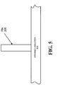
- FIG. 5 illustrates an exemplary strained insulator 505 that may, consistent with another embodiment of the present invention, be formed beneath a fin of a FinFET, such as fin 205 shown in FIGS. 2A and 2B .
- Fin 205 may be formed upon the insulating material of strained insulator 505 such that the crystalline material of fin 205 and strained insulator 505 are lattice mismatched.
- a lattice mismatch between fin 205 and strained insulator 505 produces tensile strain in fin 205 that, in turn, improves carrier mobility of the FinFET.
- any appropriate insulating material with a lattice constant that is mismatched with the crystalline material of fin 205, may be used as strained insulator 505.
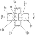
- FIG. 6 illustrates exemplary damascene source/drain regrowth consistent with another embodiment of the present invention.
- TEOS tetraethylorthosilicate
- a mask (mask 1) 610 may then be used to open a gate area 615.
- Fin 605 may be thinned down and a gate 620 may be formed by depositing and polishing polysilicon in gate area 615.
- a second mask (mask 2) 625 may be used to open a source and drain area 630.
- a nitride layer of active area 600, within the opened source and drain area 630, may be etched to expose a region of the source and drain area 630. From the exposed region, silicon can be selectively regrown to produce a source 635 and a drain 640.
Landscapes
- Thin Film Transistor (AREA)
- Insulated Gate Type Field-Effect Transistor (AREA)
Applications Claiming Priority (3)
| Application Number | Priority Date | Filing Date | Title |
|---|---|---|---|
| US10/349,042 US6803631B2 (en) | 2003-01-23 | 2003-01-23 | Strained channel finfet |
| US349042 | 2003-01-23 | ||
| PCT/US2004/000967 WO2004068585A1 (en) | 2003-01-23 | 2004-01-15 | Strained channel finfet |
Publications (2)
| Publication Number | Publication Date |
|---|---|
| EP1593161A1 EP1593161A1 (en) | 2005-11-09 |
| EP1593161B1 true EP1593161B1 (en) | 2019-04-24 |
Family
ID=32735412
Family Applications (1)
| Application Number | Title | Priority Date | Filing Date |
|---|---|---|---|
| EP04702513.5A Expired - Lifetime EP1593161B1 (en) | 2003-01-23 | 2004-01-15 | Strained channel finfet |
Country Status (7)
| Country | Link |
|---|---|
| US (2) | US6803631B2 (enExample) |
| EP (1) | EP1593161B1 (enExample) |
| JP (1) | JP2006516821A (enExample) |
| KR (1) | KR20050096155A (enExample) |
| CN (1) | CN100521230C (enExample) |
| TW (1) | TWI326489B (enExample) |
| WO (1) | WO2004068585A1 (enExample) |
Families Citing this family (95)
| Publication number | Priority date | Publication date | Assignee | Title |
|---|---|---|---|---|
| US6635909B2 (en) * | 2002-03-19 | 2003-10-21 | International Business Machines Corporation | Strained fin FETs structure and method |
| US7358121B2 (en) | 2002-08-23 | 2008-04-15 | Intel Corporation | Tri-gate devices and methods of fabrication |
| US7091068B1 (en) * | 2002-12-06 | 2006-08-15 | Advanced Micro Devices, Inc. | Planarizing sacrificial oxide to improve gate critical dimension in semiconductor devices |
| WO2004073044A2 (en) * | 2003-02-13 | 2004-08-26 | Massachusetts Institute Of Technology | Finfet device and method to make same |
| US6870179B2 (en) * | 2003-03-31 | 2005-03-22 | Intel Corporation | Increasing stress-enhanced drive current in a MOS transistor |
| TWI231994B (en) * | 2003-04-04 | 2005-05-01 | Univ Nat Taiwan | Strained Si FinFET |
| WO2004107452A1 (ja) * | 2003-05-30 | 2004-12-09 | Matsushita Electric Industrial Co., Ltd. | 半導体装置およびその製造方法 |
| US7045401B2 (en) * | 2003-06-23 | 2006-05-16 | Sharp Laboratories Of America, Inc. | Strained silicon finFET device |
| US6909151B2 (en) * | 2003-06-27 | 2005-06-21 | Intel Corporation | Nonplanar device with stress incorporation layer and method of fabrication |
| US7456476B2 (en) | 2003-06-27 | 2008-11-25 | Intel Corporation | Nonplanar semiconductor device with partially or fully wrapped around gate electrode and methods of fabrication |
| US6921982B2 (en) * | 2003-07-21 | 2005-07-26 | International Business Machines Corporation | FET channel having a strained lattice structure along multiple surfaces |
| EP1519420A2 (en) * | 2003-09-25 | 2005-03-30 | Interuniversitaire Microelectronica Centrum vzw ( IMEC) | Multiple gate semiconductor device and method for forming same |
| US6855989B1 (en) * | 2003-10-01 | 2005-02-15 | Advanced Micro Devices, Inc. | Damascene finfet gate with selective metal interdiffusion |
| US6970373B2 (en) * | 2003-10-02 | 2005-11-29 | Intel Corporation | Method and apparatus for improving stability of a 6T CMOS SRAM cell |
| US7144818B2 (en) * | 2003-12-05 | 2006-12-05 | Advanced Micro Devices, Inc. | Semiconductor substrate and processes therefor |
| US6924178B2 (en) * | 2003-12-08 | 2005-08-02 | International Business Machines Corporation | Oxide/nitride stacked in FinFET spacer process |
| US7198995B2 (en) * | 2003-12-12 | 2007-04-03 | International Business Machines Corporation | Strained finFETs and method of manufacture |
| US6936516B1 (en) * | 2004-01-12 | 2005-08-30 | Advanced Micro Devices, Inc. | Replacement gate strained silicon finFET process |
| US7268058B2 (en) * | 2004-01-16 | 2007-09-11 | Intel Corporation | Tri-gate transistors and methods to fabricate same |
| KR100781538B1 (ko) * | 2004-02-07 | 2007-12-03 | 삼성전자주식회사 | 성능이 향상된 멀티 게이트 트랜지스터용 액티브 구조의제조 방법, 이에 의해 제조된 액티브 구조 및 멀티 게이트트랜지스터 |
| US7154118B2 (en) | 2004-03-31 | 2006-12-26 | Intel Corporation | Bulk non-planar transistor having strained enhanced mobility and methods of fabrication |
| US7005302B2 (en) * | 2004-04-07 | 2006-02-28 | Advanced Micro Devices, Inc. | Semiconductor on insulator substrate and devices formed therefrom |
| US7176092B2 (en) * | 2004-04-16 | 2007-02-13 | Taiwan Semiconductor Manufacturing Company | Gate electrode for a semiconductor fin device |
| US7084018B1 (en) * | 2004-05-05 | 2006-08-01 | Advanced Micro Devices, Inc. | Sacrificial oxide for minimizing box undercut in damascene FinFET |
| US7579280B2 (en) * | 2004-06-01 | 2009-08-25 | Intel Corporation | Method of patterning a film |
| US7262104B1 (en) | 2004-06-02 | 2007-08-28 | Advanced Micro Devices, Inc. | Selective channel implantation for forming semiconductor devices with different threshold voltages |
| DE102004027691B4 (de) * | 2004-06-07 | 2008-04-30 | Infineon Technologies Ag | Verfahren zum Herstellen eines Steges aus einem Halbleitermaterial |
| US7042009B2 (en) | 2004-06-30 | 2006-05-09 | Intel Corporation | High mobility tri-gate devices and methods of fabrication |
| US7348284B2 (en) | 2004-08-10 | 2008-03-25 | Intel Corporation | Non-planar pMOS structure with a strained channel region and an integrated strained CMOS flow |
| KR100674914B1 (ko) * | 2004-09-25 | 2007-01-26 | 삼성전자주식회사 | 변형된 채널층을 갖는 모스 트랜지스터 및 그 제조방법 |
| DE102005045078B4 (de) * | 2004-09-25 | 2009-01-22 | Samsung Electronics Co., Ltd., Suwon | Feldeffekttransistor mit einer verspannten Kanalschicht an Seitenwänden einer Struktur an einem Halbleitersubstrat |
| US7332439B2 (en) | 2004-09-29 | 2008-02-19 | Intel Corporation | Metal gate transistors with epitaxial source and drain regions |
| US7422946B2 (en) | 2004-09-29 | 2008-09-09 | Intel Corporation | Independently accessed double-gate and tri-gate transistors in same process flow |
| US7361958B2 (en) | 2004-09-30 | 2008-04-22 | Intel Corporation | Nonplanar transistors with metal gate electrodes |
| JP4064955B2 (ja) * | 2004-09-30 | 2008-03-19 | 株式会社東芝 | 半導体装置及びその製造方法 |
| US20060086977A1 (en) | 2004-10-25 | 2006-04-27 | Uday Shah | Nonplanar device with thinned lower body portion and method of fabrication |
| JP2006135067A (ja) * | 2004-11-05 | 2006-05-25 | Toshiba Corp | 半導体装置およびその製造方法 |
| WO2006076151A2 (en) * | 2004-12-21 | 2006-07-20 | Carnegie Mellon University | Lithography and associated methods, devices, and systems |
| US7193279B2 (en) * | 2005-01-18 | 2007-03-20 | Intel Corporation | Non-planar MOS structure with a strained channel region |
| US7518196B2 (en) | 2005-02-23 | 2009-04-14 | Intel Corporation | Field effect transistor with narrow bandgap source and drain regions and method of fabrication |
| US20060202266A1 (en) | 2005-03-14 | 2006-09-14 | Marko Radosavljevic | Field effect transistor with metal source/drain regions |
| US7858481B2 (en) | 2005-06-15 | 2010-12-28 | Intel Corporation | Method for fabricating transistor with thinned channel |
| US7547637B2 (en) | 2005-06-21 | 2009-06-16 | Intel Corporation | Methods for patterning a semiconductor film |
| US7279375B2 (en) | 2005-06-30 | 2007-10-09 | Intel Corporation | Block contact architectures for nanoscale channel transistors |
| US7402875B2 (en) | 2005-08-17 | 2008-07-22 | Intel Corporation | Lateral undercut of metal gate in SOI device |
| US7400031B2 (en) * | 2005-09-19 | 2008-07-15 | International Business Machines Corporation | Asymmetrically stressed CMOS FinFET |
| US20070090416A1 (en) | 2005-09-28 | 2007-04-26 | Doyle Brian S | CMOS devices with a single work function gate electrode and method of fabrication |
| US7479421B2 (en) | 2005-09-28 | 2009-01-20 | Intel Corporation | Process for integrating planar and non-planar CMOS transistors on a bulk substrate and article made thereby |
| US7309626B2 (en) * | 2005-11-15 | 2007-12-18 | International Business Machines Corporation | Quasi self-aligned source/drain FinFET process |
| US7485503B2 (en) | 2005-11-30 | 2009-02-03 | Intel Corporation | Dielectric interface for group III-V semiconductor device |
| US7402856B2 (en) * | 2005-12-09 | 2008-07-22 | Intel Corporation | Non-planar microelectronic device having isolation element to mitigate fringe effects and method to fabricate same |
| DE102005059231B4 (de) * | 2005-12-12 | 2011-01-13 | Infineon Technologies Ag | Verfahren zum Herstellen eines Verbindungshalbleiter-Feldeffekttransistors mit einer Fin-Struktur und Verbindungshalbleiter-Feldeffekttransistor mit einer Fin-Struktur |
| US7439588B2 (en) * | 2005-12-13 | 2008-10-21 | Intel Corporation | Tri-gate integration with embedded floating body memory cell using a high-K dual metal gate |
| US7512017B2 (en) * | 2005-12-21 | 2009-03-31 | Intel Corporation | Integration of planar and tri-gate devices on the same substrate |
| US7396711B2 (en) | 2005-12-27 | 2008-07-08 | Intel Corporation | Method of fabricating a multi-cornered film |
| US7525160B2 (en) | 2005-12-27 | 2009-04-28 | Intel Corporation | Multigate device with recessed strain regions |
| US20070148926A1 (en) * | 2005-12-28 | 2007-06-28 | Intel Corporation | Dual halo implant for improving short channel effect in three-dimensional tri-gate transistors |
| US20070235763A1 (en) * | 2006-03-29 | 2007-10-11 | Doyle Brian S | Substrate band gap engineered multi-gate pMOS devices |
| US7407847B2 (en) * | 2006-03-31 | 2008-08-05 | Intel Corporation | Stacked multi-gate transistor design and method of fabrication |
| US7449373B2 (en) | 2006-03-31 | 2008-11-11 | Intel Corporation | Method of ion implanting for tri-gate devices |
| US7425500B2 (en) | 2006-03-31 | 2008-09-16 | Intel Corporation | Uniform silicide metal on epitaxially grown source and drain regions of three-dimensional transistors |
| US7442590B2 (en) * | 2006-04-27 | 2008-10-28 | Freescale Semiconductor, Inc | Method for forming a semiconductor device having a fin and structure thereof |
| JP2007299951A (ja) * | 2006-04-28 | 2007-11-15 | Toshiba Corp | 半導体装置およびその製造方法 |
| US20090321830A1 (en) * | 2006-05-15 | 2009-12-31 | Carnegie Mellon University | Integrated circuit device, system, and method of fabrication |
| US8143646B2 (en) | 2006-08-02 | 2012-03-27 | Intel Corporation | Stacking fault and twin blocking barrier for integrating III-V on Si |
| US7999251B2 (en) | 2006-09-11 | 2011-08-16 | International Business Machines Corporation | Nanowire MOSFET with doped epitaxial contacts for source and drain |
| US7435683B2 (en) * | 2006-09-15 | 2008-10-14 | Intel Corporation | Apparatus and method for selectively recessing spacers on multi-gate devices |
| US7700470B2 (en) | 2006-09-22 | 2010-04-20 | Intel Corporation | Selective anisotropic wet etching of workfunction metal for semiconductor devices |
| US7538391B2 (en) * | 2007-01-09 | 2009-05-26 | International Business Machines Corporation | Curved FINFETs |
| US20080173942A1 (en) * | 2007-01-22 | 2008-07-24 | International Business Machines Corporation | STRUCTURE AND METHOD OF MANUFACTURING A STRAINED FinFET WITH STRESSED SILICIDE |
| US7709893B2 (en) * | 2007-01-31 | 2010-05-04 | Infineon Technologies Ag | Circuit layout for different performance and method |
| CN102723366B (zh) * | 2007-07-27 | 2015-03-04 | 知识产权之桥一号有限责任公司 | 半导体装置 |
| US7910994B2 (en) * | 2007-10-15 | 2011-03-22 | Taiwan Semiconductor Manufacturing Company, Ltd. | System and method for source/drain contact processing |
| US8362566B2 (en) | 2008-06-23 | 2013-01-29 | Intel Corporation | Stress in trigate devices using complimentary gate fill materials |
| US8053838B2 (en) * | 2008-06-26 | 2011-11-08 | International Business Machines Corporation | Structures, fabrication methods, design structures for strained fin field effect transistors (FinFets) |
| US20100155801A1 (en) * | 2008-12-22 | 2010-06-24 | Doyle Brian S | Integrated circuit, 1T-1C embedded memory cell containing same, and method of manufacturing 1T-1C memory cell for embedded memory application |
| US7999298B2 (en) * | 2008-12-30 | 2011-08-16 | Intel Corporation | Embedded memory cell and method of manufacturing same |
| US9768305B2 (en) * | 2009-05-29 | 2017-09-19 | Taiwan Semiconductor Manufacturing Company, Ltd. | Gradient ternary or quaternary multiple-gate transistor |
| US7977174B2 (en) * | 2009-06-08 | 2011-07-12 | Globalfoundries Inc. | FinFET structures with stress-inducing source/drain-forming spacers and methods for fabricating the same |
| US20100308409A1 (en) * | 2009-06-08 | 2010-12-09 | Globalfoundries Inc. | Finfet structures with fins having stress-inducing caps and methods for fabricating the same |
| US8404592B2 (en) * | 2009-07-27 | 2013-03-26 | GlobalFoundries, Inc. | Methods for fabricating FinFET semiconductor devices using L-shaped spacers |
| US8629478B2 (en) * | 2009-07-31 | 2014-01-14 | Taiwan Semiconductor Manufacturing Company, Ltd. | Fin structure for high mobility multiple-gate transistor |
| CN102315269B (zh) * | 2010-07-01 | 2013-12-25 | 中国科学院微电子研究所 | 一种半导体器件及其形成方法 |
| CN103137671B (zh) * | 2011-12-02 | 2015-06-24 | 中芯国际集成电路制造(上海)有限公司 | 多栅极场效应晶体管及其制作方法 |
| CN103187446B (zh) * | 2011-12-31 | 2016-02-03 | 中芯国际集成电路制造(上海)有限公司 | 多栅极场效应晶体管及其制造方法 |
| US8729634B2 (en) | 2012-06-15 | 2014-05-20 | Taiwan Semiconductor Manufacturing Company, Ltd. | FinFET with high mobility and strain channel |
| EP2741337B1 (en) | 2012-12-07 | 2018-04-11 | IMEC vzw | Semiconductor heterostructure field effect transistor and method for making thereof |
| US8872225B2 (en) * | 2012-12-20 | 2014-10-28 | Intel Corporation | Defect transferred and lattice mismatched epitaxial film |
| US9029835B2 (en) * | 2012-12-20 | 2015-05-12 | Intel Corporation | Epitaxial film on nanoscale structure |
| US9391181B2 (en) * | 2012-12-21 | 2016-07-12 | Intel Corporation | Lattice mismatched hetero-epitaxial film |
| US8823060B1 (en) * | 2013-02-20 | 2014-09-02 | Taiwan Semiconductor Manufacturing Co., Ltd. | Method for inducing strain in FinFET channels |
| US9214555B2 (en) | 2013-03-12 | 2015-12-15 | Taiwan Semiconductor Manufacturing Co., Ltd. | Barrier layer for FinFET channels |
| EP3123519A4 (en) | 2014-03-24 | 2017-10-25 | Intel Corporation | Fin sculpting and cladding during replacement gate process for transistor channel applications |
| US9589811B2 (en) * | 2015-06-24 | 2017-03-07 | Varian Semiconductor Equipment Associates, Inc. | FinFET spacer etch with no fin recess and no gate-spacer pull-down |
| US9755073B1 (en) | 2016-05-11 | 2017-09-05 | International Business Machines Corporation | Fabrication of vertical field effect transistor structure with strained channels |
Family Cites Families (8)
| Publication number | Priority date | Publication date | Assignee | Title |
|---|---|---|---|---|
| US7163864B1 (en) * | 2000-10-18 | 2007-01-16 | International Business Machines Corporation | Method of fabricating semiconductor side wall fin |
| US6300182B1 (en) * | 2000-12-11 | 2001-10-09 | Advanced Micro Devices, Inc. | Field effect transistor having dual gates with asymmetrical doping for reduced threshold voltage |
| US6475869B1 (en) * | 2001-02-26 | 2002-11-05 | Advanced Micro Devices, Inc. | Method of forming a double gate transistor having an epitaxial silicon/germanium channel region |
| US20020167048A1 (en) * | 2001-05-14 | 2002-11-14 | Tweet Douglas J. | Enhanced mobility NMOS and PMOS transistors using strained Si/SiGe layers on silicon-on-insulator substrates |
| JP3782021B2 (ja) * | 2002-02-22 | 2006-06-07 | 株式会社東芝 | 半導体装置、半導体装置の製造方法、半導体基板の製造方法 |
| US6635909B2 (en) * | 2002-03-19 | 2003-10-21 | International Business Machines Corporation | Strained fin FETs structure and method |
| US6800910B2 (en) * | 2002-09-30 | 2004-10-05 | Advanced Micro Devices, Inc. | FinFET device incorporating strained silicon in the channel region |
| US6611029B1 (en) * | 2002-11-08 | 2003-08-26 | Advanced Micro Devices, Inc. | Double gate semiconductor device having separate gates |
-
2003
- 2003-01-23 US US10/349,042 patent/US6803631B2/en not_active Expired - Lifetime
-
2004
- 2004-01-15 WO PCT/US2004/000967 patent/WO2004068585A1/en not_active Ceased
- 2004-01-15 CN CNB200480002593XA patent/CN100521230C/zh not_active Expired - Fee Related
- 2004-01-15 KR KR1020057013666A patent/KR20050096155A/ko not_active Abandoned
- 2004-01-15 JP JP2006502829A patent/JP2006516821A/ja active Pending
- 2004-01-15 EP EP04702513.5A patent/EP1593161B1/en not_active Expired - Lifetime
- 2004-01-20 TW TW093101515A patent/TWI326489B/zh not_active IP Right Cessation
- 2004-04-28 US US10/833,112 patent/US6897527B2/en not_active Expired - Lifetime
Non-Patent Citations (1)
| Title |
|---|
| None * |
Also Published As
| Publication number | Publication date |
|---|---|
| US6803631B2 (en) | 2004-10-12 |
| JP2006516821A (ja) | 2006-07-06 |
| TW200423405A (en) | 2004-11-01 |
| WO2004068585A1 (en) | 2004-08-12 |
| KR20050096155A (ko) | 2005-10-05 |
| EP1593161A1 (en) | 2005-11-09 |
| US20040195627A1 (en) | 2004-10-07 |
| US6897527B2 (en) | 2005-05-24 |
| CN100521230C (zh) | 2009-07-29 |
| US20040145019A1 (en) | 2004-07-29 |
| CN1742375A (zh) | 2006-03-01 |
| TWI326489B (en) | 2010-06-21 |
Similar Documents
| Publication | Publication Date | Title |
|---|---|---|
| EP1593161B1 (en) | Strained channel finfet | |
| US6762483B1 (en) | Narrow fin FinFET | |
| US7250645B1 (en) | Reversed T-shaped FinFET | |
| US11043587B2 (en) | Fabrication of vertical fin transistor with multiple threshold voltages | |
| US6812119B1 (en) | Narrow fins by oxidation in double-gate finfet | |
| US7304336B2 (en) | FinFET structure and method to make the same | |
| US6855583B1 (en) | Method for forming tri-gate FinFET with mesa isolation | |
| US6686231B1 (en) | Damascene gate process with sacrificial oxide in semiconductor devices | |
| US8778766B2 (en) | Field effect transistor, integrated circuit element, and method for manufacturing the same | |
| US6955969B2 (en) | Method of growing as a channel region to reduce source/drain junction capacitance | |
| US7186599B2 (en) | Narrow-body damascene tri-gate FinFET | |
| US7084018B1 (en) | Sacrificial oxide for minimizing box undercut in damascene FinFET | |
| US20100207209A1 (en) | Semiconductor device and producing method thereof | |
| US7785944B2 (en) | Method of making double-gated self-aligned finFET having gates of different lengths | |
| US6855989B1 (en) | Damascene finfet gate with selective metal interdiffusion | |
| US6876042B1 (en) | Additional gate control for a double-gate MOSFET | |
| US9911601B2 (en) | Epitaxial silicon germanium fin formation using sacrificial silicon fin templates | |
| US12402394B2 (en) | Semiconductor structure |
Legal Events
| Date | Code | Title | Description |
|---|---|---|---|
| PUAI | Public reference made under article 153(3) epc to a published international application that has entered the european phase |
Free format text: ORIGINAL CODE: 0009012 |
|
| 17P | Request for examination filed |
Effective date: 20050822 |
|
| AK | Designated contracting states |
Kind code of ref document: A1 Designated state(s): AT BE BG CH CY CZ DE DK EE ES FI FR GB GR HU IE IT LI LU MC NL PT RO SE SI SK TR |
|
| AX | Request for extension of the european patent |
Extension state: AL LT LV MK |
|
| DAX | Request for extension of the european patent (deleted) | ||
| RBV | Designated contracting states (corrected) |
Designated state(s): DE FR GB |
|
| 17Q | First examination report despatched |
Effective date: 20060721 |
|
| STAA | Information on the status of an ep patent application or granted ep patent |
Free format text: STATUS: EXAMINATION IS IN PROGRESS |
|
| RAP1 | Party data changed (applicant data changed or rights of an application transferred) |
Owner name: ADVANCED MICRO DEVICES, INC. |
|
| RAP1 | Party data changed (applicant data changed or rights of an application transferred) |
Owner name: ADVANCED MICRO DEVICES, INC. |
|
| REG | Reference to a national code |
Ref country code: DE Ref legal event code: R079 Ref document number: 602004053911 Country of ref document: DE Free format text: PREVIOUS MAIN CLASS: H01L0029100000 Ipc: H01L0029780000 |
|
| GRAP | Despatch of communication of intention to grant a patent |
Free format text: ORIGINAL CODE: EPIDOSNIGR1 |
|
| STAA | Information on the status of an ep patent application or granted ep patent |
Free format text: STATUS: GRANT OF PATENT IS INTENDED |
|
| RIC1 | Information provided on ipc code assigned before grant |
Ipc: H01L 21/336 19900101ALI20181015BHEP Ipc: H01L 29/10 19740701ALI20181015BHEP Ipc: H01L 29/78 19740701AFI20181015BHEP |
|
| INTG | Intention to grant announced |
Effective date: 20181116 |
|
| RIC1 | Information provided on ipc code assigned before grant |
Ipc: H01L 29/10 20060101ALI20181015BHEP Ipc: H01L 21/336 20060101ALI20181015BHEP Ipc: H01L 29/78 20060101AFI20181015BHEP |
|
| RAP1 | Party data changed (applicant data changed or rights of an application transferred) |
Owner name: INNOVATIVE FOUNDRY TECHNOLOGIES B.V. |
|
| GRAS | Grant fee paid |
Free format text: ORIGINAL CODE: EPIDOSNIGR3 |
|
| GRAA | (expected) grant |
Free format text: ORIGINAL CODE: 0009210 |
|
| STAA | Information on the status of an ep patent application or granted ep patent |
Free format text: STATUS: THE PATENT HAS BEEN GRANTED |
|
| AK | Designated contracting states |
Kind code of ref document: B1 Designated state(s): DE FR GB |
|
| REG | Reference to a national code |
Ref country code: GB Ref legal event code: FG4D |
|
| REG | Reference to a national code |
Ref country code: DE Ref legal event code: R096 Ref document number: 602004053911 Country of ref document: DE |
|
| REG | Reference to a national code |
Ref country code: DE Ref legal event code: R097 Ref document number: 602004053911 Country of ref document: DE |
|
| PLBE | No opposition filed within time limit |
Free format text: ORIGINAL CODE: 0009261 |
|
| STAA | Information on the status of an ep patent application or granted ep patent |
Free format text: STATUS: NO OPPOSITION FILED WITHIN TIME LIMIT |
|
| 26N | No opposition filed |
Effective date: 20200127 |
|
| GBPC | Gb: european patent ceased through non-payment of renewal fee |
Effective date: 20200115 |
|
| PG25 | Lapsed in a contracting state [announced via postgrant information from national office to epo] |
Ref country code: GB Free format text: LAPSE BECAUSE OF NON-PAYMENT OF DUE FEES Effective date: 20200115 Ref country code: FR Free format text: LAPSE BECAUSE OF NON-PAYMENT OF DUE FEES Effective date: 20200131 |
|
| PGFP | Annual fee paid to national office [announced via postgrant information from national office to epo] |
Ref country code: DE Payment date: 20210621 Year of fee payment: 18 |
|
| REG | Reference to a national code |
Ref country code: DE Ref legal event code: R119 Ref document number: 602004053911 Country of ref document: DE |
|
| PG25 | Lapsed in a contracting state [announced via postgrant information from national office to epo] |
Ref country code: DE Free format text: LAPSE BECAUSE OF NON-PAYMENT OF DUE FEES Effective date: 20220802 |