EP1592142A1 - Kommunikationseinrichtung und kommunikationssystem - Google Patents
Kommunikationseinrichtung und kommunikationssystem Download PDFInfo
- Publication number
- EP1592142A1 EP1592142A1 EP04707669A EP04707669A EP1592142A1 EP 1592142 A1 EP1592142 A1 EP 1592142A1 EP 04707669 A EP04707669 A EP 04707669A EP 04707669 A EP04707669 A EP 04707669A EP 1592142 A1 EP1592142 A1 EP 1592142A1
- Authority
- EP
- European Patent Office
- Prior art keywords
- communication device
- communication
- metal layer
- opening
- data carrier
- Prior art date
- Legal status (The legal status is an assumption and is not a legal conclusion. Google has not performed a legal analysis and makes no representation as to the accuracy of the status listed.)
- Withdrawn
Links
Images




Classifications
-
- H—ELECTRICITY
- H04—ELECTRIC COMMUNICATION TECHNIQUE
- H04B—TRANSMISSION
- H04B5/00—Near-field transmission systems, e.g. inductive or capacitive transmission systems
- H04B5/20—Near-field transmission systems, e.g. inductive or capacitive transmission systems characterised by the transmission technique; characterised by the transmission medium
- H04B5/24—Inductive coupling
- H04B5/26—Inductive coupling using coils
-
- G—PHYSICS
- G06—COMPUTING OR CALCULATING; COUNTING
- G06K—GRAPHICAL DATA READING; PRESENTATION OF DATA; RECORD CARRIERS; HANDLING RECORD CARRIERS
- G06K7/00—Methods or arrangements for sensing record carriers, e.g. for reading patterns
- G06K7/10—Methods or arrangements for sensing record carriers, e.g. for reading patterns by electromagnetic radiation, e.g. optical sensing; by corpuscular radiation
- G06K7/10009—Methods or arrangements for sensing record carriers, e.g. for reading patterns by electromagnetic radiation, e.g. optical sensing; by corpuscular radiation sensing by radiation using wavelengths larger than 0.1 mm, e.g. radio-waves or microwaves
- G06K7/10158—Methods or arrangements for sensing record carriers, e.g. for reading patterns by electromagnetic radiation, e.g. optical sensing; by corpuscular radiation sensing by radiation using wavelengths larger than 0.1 mm, e.g. radio-waves or microwaves methods and means used by the interrogation device for reliably powering the wireless record carriers using an electromagnetic interrogation field
- G06K7/10178—Methods or arrangements for sensing record carriers, e.g. for reading patterns by electromagnetic radiation, e.g. optical sensing; by corpuscular radiation sensing by radiation using wavelengths larger than 0.1 mm, e.g. radio-waves or microwaves methods and means used by the interrogation device for reliably powering the wireless record carriers using an electromagnetic interrogation field including auxiliary means for focusing, repeating or boosting the electromagnetic interrogation field
-
- G—PHYSICS
- G06—COMPUTING OR CALCULATING; COUNTING
- G06K—GRAPHICAL DATA READING; PRESENTATION OF DATA; RECORD CARRIERS; HANDLING RECORD CARRIERS
- G06K7/00—Methods or arrangements for sensing record carriers, e.g. for reading patterns
- G06K7/10—Methods or arrangements for sensing record carriers, e.g. for reading patterns by electromagnetic radiation, e.g. optical sensing; by corpuscular radiation
- G06K7/10009—Methods or arrangements for sensing record carriers, e.g. for reading patterns by electromagnetic radiation, e.g. optical sensing; by corpuscular radiation sensing by radiation using wavelengths larger than 0.1 mm, e.g. radio-waves or microwaves
- G06K7/10316—Methods or arrangements for sensing record carriers, e.g. for reading patterns by electromagnetic radiation, e.g. optical sensing; by corpuscular radiation sensing by radiation using wavelengths larger than 0.1 mm, e.g. radio-waves or microwaves using at least one antenna particularly designed for interrogating the wireless record carriers
- G06K7/10336—Methods or arrangements for sensing record carriers, e.g. for reading patterns by electromagnetic radiation, e.g. optical sensing; by corpuscular radiation sensing by radiation using wavelengths larger than 0.1 mm, e.g. radio-waves or microwaves using at least one antenna particularly designed for interrogating the wireless record carriers the antenna being of the near field type, inductive coil
-
- G—PHYSICS
- G06—COMPUTING OR CALCULATING; COUNTING
- G06K—GRAPHICAL DATA READING; PRESENTATION OF DATA; RECORD CARRIERS; HANDLING RECORD CARRIERS
- G06K7/00—Methods or arrangements for sensing record carriers, e.g. for reading patterns
- G06K7/10—Methods or arrangements for sensing record carriers, e.g. for reading patterns by electromagnetic radiation, e.g. optical sensing; by corpuscular radiation
- G06K7/10009—Methods or arrangements for sensing record carriers, e.g. for reading patterns by electromagnetic radiation, e.g. optical sensing; by corpuscular radiation sensing by radiation using wavelengths larger than 0.1 mm, e.g. radio-waves or microwaves
- G06K7/10316—Methods or arrangements for sensing record carriers, e.g. for reading patterns by electromagnetic radiation, e.g. optical sensing; by corpuscular radiation sensing by radiation using wavelengths larger than 0.1 mm, e.g. radio-waves or microwaves using at least one antenna particularly designed for interrogating the wireless record carriers
- G06K7/10346—Methods or arrangements for sensing record carriers, e.g. for reading patterns by electromagnetic radiation, e.g. optical sensing; by corpuscular radiation sensing by radiation using wavelengths larger than 0.1 mm, e.g. radio-waves or microwaves using at least one antenna particularly designed for interrogating the wireless record carriers the antenna being of the far field type, e.g. HF types or dipoles
-
- H—ELECTRICITY
- H04—ELECTRIC COMMUNICATION TECHNIQUE
- H04B—TRANSMISSION
- H04B5/00—Near-field transmission systems, e.g. inductive or capacitive transmission systems
- H04B5/40—Near-field transmission systems, e.g. inductive or capacitive transmission systems characterised by components specially adapted for near-field transmission
- H04B5/48—Transceivers
Definitions
- the present invention relates to a communication device which has a transmitting/receiving section including an antenna, a control section, and a memory section and which performs communication with a data carrier by electromagnetic waves and a communication system.
- a data carrier which has an antenna coil and a memory section and which performs non-contact communication by electromagnetic waves has been employed widely in a variety of fields.
- a data carrier formed into a card shape has been employed as IC cards for a season ticket of a transportation system, a financial-related cash card, an personal identification card for opening or closing an opening/closing door ensuring security, or the like.
- these IC card is formed in such a manner that a data carrier is sandwiched between two thin protecting resin plates.
- a communication device performing electromagnetic wave communication with a data carrier is installed as a card detection section for example in an automatic ticket checker of a transport facility, an automatic money cashiers of a financial institution, an opening/closing lock mechanism for opening/closing an opening or closing door, or the like.
- each of the data carrier and communication device mutually perform non-contact communication, utilizing electromagnetic waves. That is, each of the data carrier and communication device is provided with an antenna coil, a control circuit, and a memory section to mutually perform transmission and reception of information, utilizing the antenna coil to execute a variety of managements and controls.
- the communication device is arranged on the opening/closing door or on a wall part adjoining the door, and the card-typed data carrier is brought near the communication device so that the opening/closing door is automatically unlocked when a code sent from the data carrier corresponds to a code stored in the communication device.
- the communication device is generally protected by a case or the like for the sake of durability, due to the above-described reasons, the communication device, particularly the surface part covering its antenna, is protected by a resin (plastic) case that is a non-conductive material, so as to be arranged at or installed on an object.
- the resin case has lower strength and durability than those of a metal case, it is needless to say that it is desired that the communication device is protected by a metal case if it is possible.
- the communication device is generally accommodated in a resin box attached on a surface of a door or a surface of a wall adjacent to the door, and the data carrier is brought bear the surface of the box so as to unlock it.
- the box it is undesirable to allow the box to protrude from a surface of a door or a wall from an external appearance viewpoint, and since it can be easily broken, there is a problem also from a security viewpoint.
- a system in which the communication device is arranged inside a wall employing an iron plate or the like and in which the data carrier is brought near from the wall surface to unlock an opening/closing door is disclosed in Japanese Patent Application Laid-Open No. 2003-41819.
- the communication device having a transmitting/receiving section including an antenna, a control section, and a memory section is attached inside the wall adjacent to the door so as to perform communication with the data carrier, utilizing leakage magnetic flux leaking through a fine gap of the wall of the opening/closing door to perform automatic unlocking of the door. Since the communication device is not exposed on the surface of the wall in this system, the system is excellent from external appearance and security viewpoints. However, since the communication device needs to be arranged close to the boundary part between the opening/closing door and the wall, a problem of restricted installation remains.
- the present invention is to solve the above-described problem, and it is an object of the present invention to provide a communication device which solves the problem remaining in a communication device adopting the above-mentioned magnetic flux leakage method and a communication system employing the same.
- a communication device is a communication device which has a transmitting/receiving section including an antenna, a control section, and a memory section to perform electromagnetic wave communication with a data carrier.
- the present communication device is characterized in that at least a surface side of the antenna part of the transmitting/receiving section is covered with a metal layer and that the metal layer has a material and a thickness through which electromagnetic wave communication is possible with the data carrier via the metal layer by an electromagnetic induction effect.
- the communication device since at least a surface side of the antenna part of the transmitting/receiving section that is the communication terminal part of the communication device is protected by the specific metal layer, durability of the transmitting/receiving terminal part can be improved without deteriorating a practical communication sensitivity.
- At least a communication side surface of the communication device including the transmitting/receiving section, control section, and memory section can be covered with the metal layer. With such a structure, durability of the entire communication device can be improved.
- austenitic stainless steel, titanium, or cupronickel can be employed as the material of the metal layer.
- the thickness of the metal layer can be selected from the range from 0.05 mm or greater to 1 mm or less. This thickness range can ensure a high communication sensitivity and durability reliably.
- a position display section displaying a communication position or a code display section having a code function composed of a mark, a figure, or a symbol can be provided.
- the position display section displaying the communication position is provided as described above, since the data carrier can be allowed to approach the communication position of the communication device from the surface side of the metal layer reliably, electromagnetic wave communication is possible between the communication device and the data carrier at a high communication sensitivity.
- the code display section since only a specific person which has recognized the code display section in advance can execute electromagnetic wave communication, a communication system having a high security function can be constructed.
- a communication system is a communication system which includes a data carrier having a transmitting/receiving section including an antenna, a control section, and a memory section and a communication device having a transmitting/receiving section including an antenna, a control section, and a memory section to perform electromagnetic wave communication with the data carrier.
- the present communication system is characterized in that at least a surface of the antenna part of the communication device is covered with a metal layer and that the metal layer has a material and a thickness through which electromagnetic wave communication is possible with the data carrier via the metal layer by an electromagnetic induction effect.
- the communication system can be constructed in such a manner that at least one surface of the data carrier is covered with a metal layer and that the metal layer has a material and a thickness through which electromagnetic wave communication is possible with the communication device via the metal layer by an electromagnetic induction effect. In this way, since durability of the data carrier employed in the communication system becomes high, reliability of the communication system can be further improved.
- the communication device can be installed in an opening/closing lock mechanism.
- the communication system can be constructed in such a manner that at least a surface side of the antenna part of the communication device installed is covered with the metal layer and that the control section of the communication device recognizes the difference between code information stored in the memory section of the communication device and specific code information transmitted from the data carrier so that the control section of the communication device outputs an unlock signal to the opening/closing lock mechanism when both information correspond to each other.
- the opening/closing lock mechanism can be disposed to be laid across an opening/closing door or an opening/closing lid and a metal wall adjacent thereto or a wall containing a metal material, and the communication device can be arranged on an opening part provided on the wall or is arranged inside the wall.
- the communication system of the present invention can be applied to opening/closing control for the opening/closing door or the opening/closing lid provided on a metal wall. Since providing a protruding portion on a surface of the metal wall is not needed, the system is excellent from external appearance and security viewpoints.
- a position display section displaying a communication position or a code display section having a code function composed of a mark, a figure, or a symbol can be displayed.
- the data carrier can be allowed to approach the communication position necessary for opening/closing from the surface side of the metal layer reliably.
- electromagnetic wave communication is possible between the communication device and the data carrier, ensuring a high communication sensitivity, anybody can control the opening/closing lock mechanism reliably.
- the code display section since only a specific person which has recognized the code display section in advance can execute electromagnetic wave communication, ensuring a high communication sensitivity, opening/closing control for the opening/closing lock mechanism can be executed reliably in a state in which a high security function is ensured.
- FIG. 1 a transmitting/receiving section 3 having an antenna coil 2 is provided in a communication device 1, and the entire communication device 1 is protected by a thin metal layer 4. Meanwhile, in a data carrier 5 also, a transmitting/receiving section 7 having an antenna coil 6 is provided.
- the data carrier 5 When the data carrier 5 is brought near the communication device 1, the data carrier 5 is charged with electrical power by the electromagnetic wave to become in an activated state. Then, an electromagnetic wave H1 for a response which contains a specific code or the like is transmitted from the antenna coil 6 of the activated data carrier 5 toward the antenna coil 2 of the communication device 1. Although this electromagnetic wave H1 does not reach the antenna coil 2 of the communication device 1, it allows the metal layer 4 to generate a skin current I, and by the skin current I, an electromagnetic wave H2 of the same frequency is generated in the opposite side of the metal layer 4. that is, in the antenna coil 2 side of the communication device 1.
- the frequency of the electromagnetic wave employed in the communication is variously selected from the frequency bandwidth range from several hundreds Hz to several MHz, and when such a high frequency electromagnetic wave is emitted to the metal layer 4, the skin current I is generated in the metal layer 4 as described above. It has been known that the thickness d of the skin current I is inversely proportional to ( ⁇ f ⁇ ) to a power of 1/2.
- f represents the frequency of the electromagnetic wave
- ⁇ the dielectric constant of the metal layer 4
- the thickness t of the metal layer 4 In order to perform communication by the electromagnetic induction effect through the metal layer 4, it is necessary to allow the thickness t of the metal layer 4 to be t ⁇ d, and it has been known that the smaller the value of the thickness t of the metal layer 4 compared to the thickness d of the skin current I, the more the communication sensitivity is improved, where the thickness d of the skin current I is constant.
- the thinner the thickness t of the metal layer 4 that is, the thinner, the more deteriorated the strength thereof, and when it reaches a limit, a protective function thereof cannot be performed.
- an austenitic stainless steel, cupronickel, titanium, or the like is suitable for such a purpose. Further, brass or the like is also employable. Meanwhile, the values of the thickness d of the skin current I of iron, aluminum, copper, nickel, or the like are small, and thus communication is difficult unless they are made thin to the extent of foil.
- Table 1 shown below is experiment results obtained by measuring a non-contacting communicable distance with respect to a data carrier structure in which austenitic stainless steel plate (SUS 301. 304, 316) and ferrite stainless steel plate (SUS 430) are employed as the metal plate forming the metal layer 4.
- austenitic stainless steel plate SUS 301. 304, 316
- ferrite stainless steel plate SUS 430
- Table 1 the value obtained by multiplying the plate thickness of each type of metal plate by the number of stacked layers is shown as the layer thickness of the entire metal layer 4, and the size of each metal plate forming the metal layer 4 is set at a sufficient one by which magnetic flux does not leak from an end portion.
- "X" represents a case where reading was not possible.
- Table 2 shown below is experiment results obtained by conducting a method similar to that of Table 1 with respect to an iron plate, copper plate, cupronickel plate, nickel plate, titanium plate, aluminum plate, and brass plate.
- the metal layer 4 As shown in Tables 1 and 2 above, as a material of the metal layer 4, austenitic stainless steel, cupronickel, titanium, and the like are preferred as the metal layer 4 protecting the communication device 1 of the present invention, and in the case where such a metal is employed, the thickness of the metal layer 4 is preferred to be appropriately selected from the range from 0.05 mm or greater to 1 mm or less.
- a metal layer having a material and a thickness through which electromagnetic wave communication is possible by the electromagnetic induction effect means that the metal layer 4 having a material and a thickness through which such a function can be demonstrated.
- the thickness is on the order of about 0.015 mm in the case where the material of the metal layer 4 is aluminum and when the thickness is on the order of about 0.05 mm in the case of copper.
- These metals have functions of moisturc-proofing, light-shielding, and the like and can be utilized as the metal layer 4 of the present invention.
- a thin aluminum or copper is employed as the metal layer 4, it is also possible to improve the strength thereof by stacking appropriate resin substrates or resin sheets on a side surface or both surfaces thereof to reinforce it.
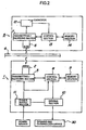
- FIG. 2 is a block diagram explaining an opening/closing system of an opening/closing door constructed by a communication system according to the present invention utilizing the electromagnetic wave communication principle of the communication device 1.
- the communication device 1 is provided with the transmitting/receiving section 3 having the antenna coil 2, the control section 8 controlling transmission/reception of this transmitting/receiving section 3, a memory section 9 connected with the control section 8, a driving section 10 which receives a control signal from the control section 8 to output a drive signal to an opening/closing lock device 30 of an opening/closing door 20 shown in FIGS. 4 and 5, and a power supply section 11 which receives an external AC power source to supply a DC power source to the above-mentioned equipment.
- the transmitting/receiving section 3, the control section 8, and the memory section 9 can be composed of a microcomputer, the power supply section 11 can be composed of a small-sized diode and a capacitor, and the driving section 10 can be composed of a thyristor circuit. It is desired that the antenna coil 2 of the communication device 1 has a disk type coil shape which can make the communication sensitivity high easily.
- the data carrier 5 is provided with the transmitting/receiving section 7 having the antenna coil 6, an electrical power accumulating capacitor 12 connected with the transmitting/receiving section 7, a control section 13 controlling transmission/rcccption of the transmitting/receiving section 7, and a memory section 14 connected to the control section 13.
- the transmitting/receiving section 7, the capacitor 12, the control section 13, and the memory section 14 can be composed of a one-chip IC, and the antenna coil 6 is connected with this IC chip.
- the data carrier 5 employed may be either a card type or a stick-like key type. It is preferred that in the case of a card type, an antenna coil 6 having a disk type coil shape is employed, and in the case of a key type, an antenna coil 6 having a thin stick-like coil is employed.
- the received specific code information is compared and checked with the code information stored in the memory section 9 in advance by the control section 8 so that the difference between the two is recognized, and when the both information correspond to each other, the control signal is outputted from the control section 8 to the drive section 10 so that an unlock signal is outputted from the drive section 10 to the opening/closing lock device 30 shown in FIG. 5.
- the control signal for unlocking is not outputted from the control section 8.
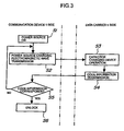
- FIG. 3 is a flow chart showing operations of the opening/closing system.
- the control section 8 of the communication device 1 controls the transmitting/receiving section 3 so as to repeatedly transmit an electromagnetic wave for charging the power supply of the data carrier 5 at relatively short time intervals (step S2).
- the data carrier 5 If the data carrier 5 approaches the communication device 1, the data carrier 5 receives the electromagnetic wave by the antenna coil 6 thereof to allow the transmitting/receiving section 7 to be in an operation state and to charge the electrical energy of the electromagnetic wave in the capacitor 12 as electrical power. If the capacitor 12 is charged so that the circuit's voltage increases to a normal voltage, the control section 13 becomes in the operation state (step S3).
- the control section 13 transmits the unlocking specific code information stored in the memory section 14 from the transmitting/receiving section 7 to the communication device 1 (step S4).
- the communication device 1 which has received the code information compares and checks the code information with the code information which the control section 8 has allowed the memory section 9 to store as described above (step S5), and if the both code information correspond to each other, the unlocking control signal (unlocking signal) is outputted so that the opening/closing lock device 30 unlocks the opening/closing door 20 (step S6). If the both code information do not correspond to each other, the control signal (unlocking signal) is not outputted to return to step S2, so that the power source charging electromagnetic wave transmission is repeated.
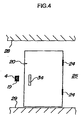
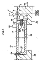
- FIGS. 4 and 5 are a front view and a side cross-sectional view showing one example of a case where the opening/closing system utilizing the communication system according to the present invention is applied to the opening/closing door of a targeted building composed of a metal material and to a wall 25 adjacent thereto
- FIG. 4 is a front view seen from the outside of the opening/closing door 20.
- the opening/closing door 20 of the building is composed of a front side plate 21 and a back side plate 22 made of an iron plate and side plates 23 coupling with these, and one side plate 23 is openably/closably coupled with the wall 25 by means of a plurality of hinge members 24.
- the wall 25 is composed of a thick base portion 26 made of reinforced concrete and a covering plate 27 made of a relatively thin iron plate constituting a metal layer covering the surface of the base portion 26, and is constructed upright between a ceiling part 28 and a floor part 29 as shown in FIG. 4.
- the communication device 1 and a driving section 31 of the opening/closing lock device 30 are disposed inside the targeted wall 25. These communication device 1 and opening/closing lock device 30 are inserted into a space part formed inside the wall 25 from the back side and are detachably secured to a peripheral wall part
- the driving section 31 of the opening/closing lock device 30 is constructed for example of an electromagnetic drive type cylinder, and a distal end of a drive shaft 32 of the driving section 31 is inserted into or retracted from a receiving portion 33 provided in the side plate 23 of the opening/closing door 20 to lock or unlock the door.
- a knob 34 for allowing a hand to do an opening/closing operation is provided on the opening/closing door 20 as shown in FIGS. 4 and 5. Further, an unillustrated manually operated lever for locking the opening/closing lock device 30 toward a lock side is provided in the back side of the opening/closing door 20.
- the communication device 1 is arranged adjacent to the covering plate 27 so that a communication side of the communication device 1, that is, the antenna 2 side, approaches the surface side of the wall 25 as shown in FIG. 5.
- the entire communication device 1 including the transmitting/receiving section 3, the control section 8, and the memory section 9 is protected by the covering plate 27.
- the communication device 1 is arranged on the surface side of the targeted wall 25 via the covering plate 27 constituting the metal layer having a material and a thickness described above through which communication is possible with the data carrier 5 by the electromagnetic induction effect.
- the opening/closing lock device 30 is disposed between the opcning/closing door 20 made of a metal material and the wall 25 adjacent thereto, and the opening/closing lock device 30 disposed in the targeted wall 25 made of a metal material is opened/closed without contacting the data carrier 5.
- the covering plate 27 facing the communication side of the communication device 1 does not achieve the function of the above-described "the metal layer having a material and a thickness through which communication is possible by an electromagnetic induction effect", for example in a case of a thick iron plate or the like, such a part is opened so that the metal layer 4 suitable for the communication device 1 of the present invention as shown in FIGS. 4 and 5 is bonded by welding or the like.
- the material of the metal layer 4 is appropriately selected from the group consisting of austenitic stainless, titanium, and cupronickel, and the layer thickness is also appropriately selected from the range from 0.05 mm or greater to 1 mm or less.
- the surface side of the antenna coil 2 which is the communication side surface of the communication device 1 and which constitutes the antenna part is covered by the metal layer 4.
- a position display section displaying a communication position or a code display section displaying a mark 19, a figure, a symbol, or the like having a code function.
- the position display section which is provided on the surface of the metal layer 4 covering the communication side surface of the communication device 1 and which shows the communication position is not limited to a specific configuration as far as it has discriminability such as a projecting portion, character, figure, symbol, pattern, color, or the like.
- the mark 19 shown in FIGS. 4 and 5 is formed by coloring which is different from the ground color of the metal layer 4.
- the opening/closing lock mechanism in which the communication device 1 is installed is disposed to be laid across the opening/closing door 20 and the wall 25 containing the covering plate 27 made of a metal material adjacent to the opening/closing door 20, and the communication device I is disposed inside the wall 25.
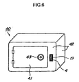
- a safe 40 made of a metal material is constructed to be a sealing type which is provided with a front opening/closing lid (opening/closing door) 41 and a peripheral wall 42, and a dial knob 43 which can unlock the lid by checking the number is provided on the opening/closing lid.
- a driving section 45 of the communication device 1 and an opening/closing lock device 44 is arranged inside the safe 40.
- a small opening portion 42a is provided on the wall 42 adjacent to the dial knob 43 of the opening/closing lid 41, and the communication device 1 is arranged on the opening portion 42a. At that time, the communication side of the communication device 1 is disposed so as to be in the surface side of the wall 42.
- a non-conductive fire-proof layer 46 lies between the communication device 1 and the metal layer 4 provided on a part of the surface side of the wall 42.
- the driving section 45 is for example composed of an electromagnetic drive type cylinder, and a distal end of a drive shaft 47 of the driving section 45 is inserted into or retracted from a receiving portion 48 provided upon the opening/closing lid 41 to lock or unlock the door.
- the opening/closing lock device 44 is arranged between the opening/closing lid 41 of the safe 40 formed of a metal material and the wall 42 adjacent thereto, and this opening/closing lock device 44 is automatically locked to the lock side when the opening/closing lid 41 is closed.
- the opening/closing lock mechanism in which the communication device 1 is installed is disposed to be laid across the opening/closing lid 41 and the wall 42 made of a metal material adjacent to this opening/closing lid 41, and the communication device 1 is disposed on the opening portion 42a arranged on the wall 42.
- a position display section displaying a communication position or a code display section displaying a mark 19, a figure, a symbol, or the like having a code function.
- FIG. 8A and 8B is one example in which a data carrier structure A is formed into a card shape.
- Reference numeral 4 denotes a metal layer provided on both surfaces of the data carrier 5, reference numeral 6 a circular antenna coil formed by winding a lead wire around an air core coil as shown in FIG. 9, reference numeral 51 a semiconductor 1C chip (control chip) composed of an integrated circuit, and reference numeral 52 a resin layer.
- the data carrier 5 which is a circular or ring shape shown in FIG. 9, the data carrier which an antenna coil 6 composed of a circular air core coil and the semiconductor IC chip 51 connected thereto are formed by embedding in resin to be entirely molded and has an outer diameter of the order of 10 to 50 mm and a thickness of the order of 0.7 to 12.0 mm is on the market.
- a model of Logi Tag and the like marketed by Hanex Co., Ltd is applicable.
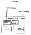
- the semiconductor IC chip 51 as shown in FIG. 10, has the control section 13 such as a CPU (central processing unit) and the like, the memory section 14 such as a memory and the like having a writable non-volatile storage clement, the transmitting/receiving section 7, and the electrical power accumulating capacitor 12.
- the control section 13 such as a CPU (central processing unit) and the like
- the memory section 14 such as a memory and the like having a writable non-volatile storage clement
- the transmitting/receiving section 7 and the electrical power accumulating capacitor 12.
- a transmitting/receiving method of the data carrier 5 will be explained with reference to FIG. 10.
- the communication device 1 such as a read/write device and the like in a first step transmits an electromagnetic wave for calling the data carrier 5 and for transmitting electrical power
- the data carrier 5 receives the electromagnetic wave through a tuning operation of the transmitting/receiving section 7 composed of the antenna coil 6 and a transmitting/receiving circuit, and the electrical power is stored in the capacitor 12.
- an elcctromagnctic wave for reading is transmitted from the communication device 1 to the data carrier 5.
- the electromagnetic wave is inputted from the antenna coil 6 of the data carrier 5 to the control section 13 via the transmitting/receiving section 7, and according to the input the control section 13 reads necessary information out of the memory section 14 to allow the information to be transmitted from the transmitting/receiving section 7 to the communication device 1 via the antenna coil 6 as an electromagnetic wave.
- the control section 13 reads necessary information out of the memory section 14 to allow the information to be transmitted from the transmitting/receiving section 7 to the communication device 1 via the antenna coil 6 as an electromagnetic wave.
- data is written in the memory section 14 of the data carrier 5 from the communication device 1 also, such an operation is performed in accordance with the above-described method. These series of steps are performed roughly instantly.
- the electromagnetic wave can be represented by an electric field and a magnetic field which have a phase difference of 90 degree, to be transmitted alternatingly, and transmission/reception is performed utilizing current (high frequency current) flowing in the antenna coil 6 by allowing the magnetic field and the antenna coil 6 to intersect with each other.
- a high frequency magnetic field component is distributed as a loop (magnetic flux loop) passing through the center of the antenna coil 6 by the high frequency current flowing in the antenna coil 6, and when the antenna coil 2 of the communication device 1 is placed in this magnetic flux area, the communication device 1 can receive information from the data carrier 5.
- the magnetic field component is distributed around the antenna coil 6 of the data carrier 5 so that the antenna coil 6 receives it.
- the data carrier 5 is formed by being molded by a resin layer 52 in a state in which the semiconductor IC chip 51 is connected to the circular antenna coil 6, and is formed into a card shape in such a manner that a metal layer 4 which is for example made of austenitic stainless steel plate, titanium plate, or cupronickel plate and whose thickness is selected from the range from 0.05 mm or greater to 1 mm or less is allowed to adhere to both surfaces of the data carrier 5 by gluing or the like.
- a metal layer 4 which is for example made of austenitic stainless steel plate, titanium plate, or cupronickel plate and whose thickness is selected from the range from 0.05 mm or greater to 1 mm or less is allowed to adhere to both surfaces of the data carrier 5 by gluing or the like.
- the card shaped data carrier structure A since the surface thereof is covered with the metal layer 4, it can be utilized as an IC card.
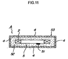
- FIGS. 11 and 12 show another example of the data carrier structure A.
- the data carrier 5 (see FIG. 9A and 9B) having the circular antenna coil 2 or a data carrier 5 having a circular shape antenna coil 2 as shown in FIG. 12 is respectively accommodated inside a vessel 53 formed by the metal layer 4 made of an austenitic stainless steel plate, and its space is filled with a resin layer 52 to be sealed.
- the data carrier 5 shown in FIG. 12 has a cylindrical rod antenna formed by densely winding an antenna coil 2 around the outer periphery of a cylindrical core member 54 such as an iron core, ferrite, or the like formed into a rod shape by single line winding in a spiral shape in the axial direction thereof (horizontal direction in FIG. 12), and is constructed by allowing both ends of the antenna coil 2 to be connected to the semiconductor IC chip 51 constituted by an integrated circuit.
- a cylindrical rod antenna formed by densely winding an antenna coil 2 around the outer periphery of a cylindrical core member 54 such as an iron core, ferrite, or the like formed into a rod shape by single line winding in a spiral shape in the axial direction thereof (horizontal direction in FIG. 12), and is constructed by allowing both ends of the antenna coil 2 to be connected to the semiconductor IC chip 51 constituted by an integrated circuit.
- the data carrier 5 which is entirely formed into a rod shape
- the data carrier which is formed by sealing a rod antenna part including the core member 54 and the antenna coil 2 and the semiconductor IC chip 51 composed of an integrated circuit in a slender glass vessel and which is miniaturized so as to have an outer diameter on the order of several millimeters and a total length on the order of ten and several millimeters to several tens millimeters is on the market.
- this type of data carrier there is Glass Tag marketed by Hanex Co., Ltd as a RFID tag, and it has an outer diameter of 2 to 4 mm and a length on the order of 12 to 15 mm so that it is exceedingly compact.
Landscapes
- Engineering & Computer Science (AREA)
- Physics & Mathematics (AREA)
- Health & Medical Sciences (AREA)
- Toxicology (AREA)
- Computer Networks & Wireless Communication (AREA)
- Electromagnetism (AREA)
- General Health & Medical Sciences (AREA)
- Artificial Intelligence (AREA)
- Computer Vision & Pattern Recognition (AREA)
- General Physics & Mathematics (AREA)
- Theoretical Computer Science (AREA)
- Signal Processing (AREA)
- Near-Field Transmission Systems (AREA)
- Lock And Its Accessories (AREA)
Applications Claiming Priority (3)
| Application Number | Priority Date | Filing Date | Title |
|---|---|---|---|
| JP2003030437A JP4430874B2 (ja) | 2003-02-07 | 2003-02-07 | 通信装置及び開閉システム |
| JP2003030437 | 2003-02-07 | ||
| PCT/JP2004/001077 WO2004070966A1 (ja) | 2003-02-07 | 2004-02-03 | 通信装置及び通信システム |
Publications (2)
| Publication Number | Publication Date |
|---|---|
| EP1592142A1 true EP1592142A1 (de) | 2005-11-02 |
| EP1592142A4 EP1592142A4 (de) | 2007-09-19 |
Family
ID=32844268
Family Applications (1)
| Application Number | Title | Priority Date | Filing Date |
|---|---|---|---|
| EP04707669A Withdrawn EP1592142A4 (de) | 2003-02-07 | 2004-02-03 | Kommunikationseinrichtung und kommunikationssystem |
Country Status (4)
| Country | Link |
|---|---|
| US (1) | US20060119534A1 (de) |
| EP (1) | EP1592142A4 (de) |
| JP (1) | JP4430874B2 (de) |
| WO (1) | WO2004070966A1 (de) |
Cited By (3)
| Publication number | Priority date | Publication date | Assignee | Title |
|---|---|---|---|---|
| WO2006134082A1 (fr) * | 2005-06-13 | 2006-12-21 | Mbbs Holding Sa | Transpondeur passif compact |
| GB2455628A (en) * | 2007-12-14 | 2009-06-17 | Wireless Fibre Systems Ltd | Inductive coupler operating through an electrically conductive barrier |
| EP4096105A1 (de) | 2021-05-25 | 2022-11-30 | Aiut Sp. z o.o. | Verfahren zur digitalen drahtlosen kommunikation durch eine barriere aus leitfähigem material, system zur durchführung einer solchen kommunikation und system zur überwachung des zylinderinhalts |
Families Citing this family (16)
| Publication number | Priority date | Publication date | Assignee | Title |
|---|---|---|---|---|
| US7588184B2 (en) | 2003-01-03 | 2009-09-15 | American Express Travel Related Services Company, Inc. | Metal-containing transaction card and method of making the same |
| US8033457B2 (en) | 2003-01-03 | 2011-10-11 | American Express Travel Related Services Company, Inc. | Metal-containing transaction card and method of making the same |
| JP4365326B2 (ja) * | 2003-01-03 | 2009-11-18 | アメリカン エクスプレス トラベル リレイテッド サービシーズ カンパニー, インコーポレイテッド | 金属を包含したトランザクションカード及びそれを作成する方法 |
| US7823777B2 (en) | 2003-01-03 | 2010-11-02 | American Express Travel Related Services Company, Inc. | Metal-containing transaction card and method of making same |
| WO2007089828A2 (en) * | 2006-01-31 | 2007-08-09 | Solidica, Inc. | Covert intelligent networked sensors and other fully encapsulated circuits |
| ITTO20070563A1 (it) * | 2007-07-30 | 2009-01-31 | St Microelectronics Srl | Dispositivo di identificazione a radiofrequenza con antenna accoppiata in near field |
| JP5244042B2 (ja) * | 2009-07-23 | 2013-07-24 | サイエス株式会社 | Icカードリーダ及び扉開閉装置 |
| US20120203620A1 (en) | 2010-11-08 | 2012-08-09 | Douglas Howard Dobyns | Techniques For Wireless Communication Of Proximity Based Marketing |
| US8929809B2 (en) | 2011-03-22 | 2015-01-06 | Radeum, Inc. | Techniques for wireless communication of proximity based content |
| US8880100B2 (en) | 2011-03-23 | 2014-11-04 | Radium, Inc. | Proximity based social networking |
| JP5392861B2 (ja) * | 2011-05-16 | 2014-01-22 | ソニー株式会社 | 電力供給装置および方法、電力供給システム、並びにプログラム |
| WO2013153736A1 (ja) * | 2012-04-10 | 2013-10-17 | パナソニック株式会社 | 無線電力伝送装置、送電装置、および受電装置 |
| CN105453113A (zh) * | 2013-08-15 | 2016-03-30 | 富士通株式会社 | Rfid标签及其制造方法 |
| US9705564B2 (en) | 2014-08-29 | 2017-07-11 | Freelinc Technologies | Spatially enabled secure communications |
| US10164685B2 (en) | 2014-12-31 | 2018-12-25 | Freelinc Technologies Inc. | Spatially aware wireless network |
| CN107609445B (zh) * | 2017-10-03 | 2020-05-05 | 浩德科技股份有限公司 | 一种识别rfid钱箱内款项金额的系统和方法 |
Family Cites Families (4)
| Publication number | Priority date | Publication date | Assignee | Title |
|---|---|---|---|---|
| US7002475B2 (en) * | 1997-12-31 | 2006-02-21 | Intermec Ip Corp. | Combination radio frequency identification transponder (RFID tag) and magnetic electronic article surveillance (EAS) tag |
| JP3481835B2 (ja) * | 1997-10-30 | 2003-12-22 | 株式会社アルファ | 非接触型の錠制御装置 |
| US6577226B1 (en) * | 1999-04-27 | 2003-06-10 | Trw Inc. | System and method for automatic vehicle unlock initiated via beam interruption |
| JP3894688B2 (ja) * | 1999-10-13 | 2007-03-22 | ローム株式会社 | 通信装置 |
-
2003
- 2003-02-07 JP JP2003030437A patent/JP4430874B2/ja not_active Expired - Fee Related
-
2004
- 2004-02-03 EP EP04707669A patent/EP1592142A4/de not_active Withdrawn
- 2004-02-03 WO PCT/JP2004/001077 patent/WO2004070966A1/ja not_active Ceased
- 2004-02-03 US US10/544,714 patent/US20060119534A1/en not_active Abandoned
Cited By (7)
| Publication number | Priority date | Publication date | Assignee | Title |
|---|---|---|---|---|
| WO2006134082A1 (fr) * | 2005-06-13 | 2006-12-21 | Mbbs Holding Sa | Transpondeur passif compact |
| GB2455628A (en) * | 2007-12-14 | 2009-06-17 | Wireless Fibre Systems Ltd | Inductive coupler operating through an electrically conductive barrier |
| GB2455628B (en) * | 2007-12-14 | 2012-09-05 | Wfs Technologies Ltd | Inductive coupler operating through an electrically conductive barrier |
| US8364079B2 (en) | 2007-12-14 | 2013-01-29 | Wfs Technologies Ltd. | Communication through a barrier |
| EP4096105A1 (de) | 2021-05-25 | 2022-11-30 | Aiut Sp. z o.o. | Verfahren zur digitalen drahtlosen kommunikation durch eine barriere aus leitfähigem material, system zur durchführung einer solchen kommunikation und system zur überwachung des zylinderinhalts |
| WO2022249024A1 (en) | 2021-05-25 | 2022-12-01 | AIUT Sp. z o. o. | Method for digital wireless communication through a barrier made of conductive material, system for performing such communication, and system for monitoring the level of fluid content in metal container |
| US12587233B2 (en) | 2021-05-25 | 2026-03-24 | AIUT Sp. z o. o. | Method for digital wireless communication through a barrier made of conductive material, system for performing such communication, and system for monitoring the level of fluid content in metal container |
Also Published As
| Publication number | Publication date |
|---|---|
| EP1592142A4 (de) | 2007-09-19 |
| US20060119534A1 (en) | 2006-06-08 |
| WO2004070966A1 (ja) | 2004-08-19 |
| JP2004266352A (ja) | 2004-09-24 |
| JP4430874B2 (ja) | 2010-03-10 |
Similar Documents
| Publication | Publication Date | Title |
|---|---|---|
| EP1592142A1 (de) | Kommunikationseinrichtung und kommunikationssystem | |
| CN102714054B (zh) | 信息存储和处理装置 | |
| EP1521206B1 (de) | Weiterleitungsvorrichtung und Kommunikationssystem | |
| US8089341B2 (en) | Management system | |
| US5841122A (en) | Security structure with electronic smart card access thereto with transmission of power and data between the smart card and the smart card reader performed capacitively or inductively | |
| EP1511121B1 (de) | Rahmenantennenvorrichtung | |
| CN101529654B (zh) | 天线装置 | |
| US7375631B2 (en) | Enabling and disabling a wireless RFID portable transponder | |
| EP1308883A1 (de) | Rfid-etiketten-gehäusestruktur, rfid-etiketten-installationsstruktur und rfid-etiketten-kommunikationsverfahren | |
| US6335906B1 (en) | Portable object, in particular a watch, including multiple selectable electronic modules | |
| BR9913043B1 (pt) | processos para ordenar um grupo de itens desordenados possuindo elementos de identificação por radiofrequência, para usar um dispositivo de identificação por radiofrequência seguro na mão para ler informação de um elemento de identificação por radiofrequência, e para usar um dispositivo de identificação por radiofrequência para identificar e localizar itens possuindo um elemento de identificação por radiofrequência. | |
| US20260070440A1 (en) | Electric vehicle charging system and connector having an rfid reader and method for rf validation for charging electric vehicle | |
| EP0775082A1 (de) | In einem kraftfahrzeug montiertes automatisches betankungs- und messsystem | |
| CN112154457B (zh) | 交通工具辨识装置 | |
| US20090140837A1 (en) | RF Token and Receptacle System and Method | |
| JP2009505287A (ja) | 非接触型近接通信装置および方法 | |
| US20100238032A1 (en) | Shipping container integrity device and system | |
| JP2006126901A (ja) | タグ及びrfidシステム | |
| KR20010040777A (ko) | 고주파 식별 보안장치 | |
| JP4303529B2 (ja) | 電磁波通信システム | |
| JPH062456A (ja) | 電子ロック装置 | |
| JP2003041819A (ja) | 開閉システム | |
| JP2003129714A (ja) | キーシステム | |
| CN101282633B (zh) | 一种能至少屏蔽一张非接触智能卡或rfid标签的方法和装置 | |
| JP4690640B2 (ja) | データキャリアのセキュリティを確保する方法 |
Legal Events
| Date | Code | Title | Description |
|---|---|---|---|
| PUAI | Public reference made under article 153(3) epc to a published international application that has entered the european phase |
Free format text: ORIGINAL CODE: 0009012 |
|
| 17P | Request for examination filed |
Effective date: 20050805 |
|
| AK | Designated contracting states |
Kind code of ref document: A1 Designated state(s): AT BE BG CH CY CZ DE DK EE ES FI FR GB GR HU IE IT LI LU MC NL PT RO SE SI SK TR |
|
| AX | Request for extension of the european patent |
Extension state: AL LT LV MK |
|
| DAX | Request for extension of the european patent (deleted) | ||
| RBV | Designated contracting states (corrected) |
Designated state(s): DE FR GB |
|
| A4 | Supplementary search report drawn up and despatched |
Effective date: 20070820 |
|
| STAA | Information on the status of an ep patent application or granted ep patent |
Free format text: STATUS: THE APPLICATION IS DEEMED TO BE WITHDRAWN |
|
| 18D | Application deemed to be withdrawn |
Effective date: 20070901 |