EP1590905B1 - Signalverarbeitungssystem mit basisbandrauschmodulation und rauschrückfaltungsreduktion - Google Patents
Signalverarbeitungssystem mit basisbandrauschmodulation und rauschrückfaltungsreduktion Download PDFInfo
- Publication number
- EP1590905B1 EP1590905B1 EP04704054A EP04704054A EP1590905B1 EP 1590905 B1 EP1590905 B1 EP 1590905B1 EP 04704054 A EP04704054 A EP 04704054A EP 04704054 A EP04704054 A EP 04704054A EP 1590905 B1 EP1590905 B1 EP 1590905B1
- Authority
- EP
- European Patent Office
- Prior art keywords
- input signal
- signal
- baseband
- frequency
- dac
- Prior art date
- Legal status (The legal status is an assumption and is not a legal conclusion. Google has not performed a legal analysis and makes no representation as to the accuracy of the status listed.)
- Expired - Lifetime
Links
Images


Classifications
-
- H—ELECTRICITY
- H03—ELECTRONIC CIRCUITRY
- H03M—CODING; DECODING; CODE CONVERSION IN GENERAL
- H03M3/00—Conversion of analogue values to or from differential modulation
- H03M3/30—Delta-sigma modulation
- H03M3/322—Continuously compensating for, or preventing, undesired influence of physical parameters
- H03M3/324—Continuously compensating for, or preventing, undesired influence of physical parameters characterised by means or methods for compensating or preventing more than one type of error at a time, e.g. by synchronisation or using a ratiometric arrangement
- H03M3/326—Continuously compensating for, or preventing, undesired influence of physical parameters characterised by means or methods for compensating or preventing more than one type of error at a time, e.g. by synchronisation or using a ratiometric arrangement by averaging out the errors
- H03M3/338—Continuously compensating for, or preventing, undesired influence of physical parameters characterised by means or methods for compensating or preventing more than one type of error at a time, e.g. by synchronisation or using a ratiometric arrangement by averaging out the errors by permutation in the time domain, e.g. dynamic element matching
- H03M3/34—Continuously compensating for, or preventing, undesired influence of physical parameters characterised by means or methods for compensating or preventing more than one type of error at a time, e.g. by synchronisation or using a ratiometric arrangement by averaging out the errors by permutation in the time domain, e.g. dynamic element matching by chopping
-
- H—ELECTRICITY
- H03—ELECTRONIC CIRCUITRY
- H03F—AMPLIFIERS
- H03F1/00—Details of amplifiers with only discharge tubes, only semiconductor devices or only unspecified devices as amplifying elements
- H03F1/02—Modifications of amplifiers to raise the efficiency, e.g. gliding Class A stages, use of an auxiliary oscillation
-
- H—ELECTRICITY
- H03—ELECTRONIC CIRCUITRY
- H03F—AMPLIFIERS
- H03F1/00—Details of amplifiers with only discharge tubes, only semiconductor devices or only unspecified devices as amplifying elements
- H03F1/26—Modifications of amplifiers to reduce influence of noise generated by amplifying elements
-
- H—ELECTRICITY
- H03—ELECTRONIC CIRCUITRY
- H03F—AMPLIFIERS
- H03F3/00—Amplifiers with only discharge tubes or only semiconductor devices as amplifying elements
- H03F3/20—Power amplifiers, e.g. Class B amplifiers, Class C amplifiers
- H03F3/21—Power amplifiers, e.g. Class B amplifiers, Class C amplifiers with semiconductor devices only
- H03F3/211—Power amplifiers, e.g. Class B amplifiers, Class C amplifiers with semiconductor devices only using a combination of several amplifiers
-
- H—ELECTRICITY
- H03—ELECTRONIC CIRCUITRY
- H03F—AMPLIFIERS
- H03F3/00—Amplifiers with only discharge tubes or only semiconductor devices as amplifying elements
- H03F3/20—Power amplifiers, e.g. Class B amplifiers, Class C amplifiers
- H03F3/21—Power amplifiers, e.g. Class B amplifiers, Class C amplifiers with semiconductor devices only
- H03F3/217—Class D power amplifiers; Switching amplifiers
- H03F3/2175—Class D power amplifiers; Switching amplifiers using analogue-digital or digital-analogue conversion
-
- H—ELECTRICITY
- H03—ELECTRONIC CIRCUITRY
- H03F—AMPLIFIERS
- H03F3/00—Amplifiers with only discharge tubes or only semiconductor devices as amplifying elements
- H03F3/38—DC amplifiers with modulator at input and demodulator at output; Modulators or demodulators specially adapted for use in such amplifiers
-
- H—ELECTRICITY
- H03—ELECTRONIC CIRCUITRY
- H03F—AMPLIFIERS
- H03F2200/00—Indexing scheme relating to amplifiers
- H03F2200/331—Sigma delta modulation being used in an amplifying circuit
-
- H—ELECTRICITY
- H03—ELECTRONIC CIRCUITRY
- H03M—CODING; DECODING; CODE CONVERSION IN GENERAL
- H03M3/00—Conversion of analogue values to or from differential modulation
- H03M3/30—Delta-sigma modulation
- H03M3/50—Digital/analogue converters using delta-sigma modulation as an intermediate step
Definitions
- the present invention relates in general to the field of signal processing, and, more specifically, to a system and method for modulating baseband noise and reducing noise that occurs, in part, due to non-ideal system properties that mix noise into a baseband via fold back mechanisms.
- DAC digital-to-analog converters
- quantization noise quantization noise
- the digital to analog conversion process often involves oversampling a digital signal, modulating the signal using a delta-sigma modulator to shape noise associated with the digital signal, and performing a digital to analog conversion using a low-pass filter.
- the filtered output signal is generally amplified to produce an analog signal suitable for driving a load.
- Delta-sigma modulators receive an input signal and convert the signal into a series of binary pulses having an average amplitude over time proportional to the input signal.
- delta-sigma modulators introduce quantization noise into the modulated input signal.
- the quantization noise advantageously resides outside of the audio baseband where frequency components of interest reside, i.e. between about 0 Hz and above about 20-25 kHz.
- some post modulation processing such as a post-modulation digital to analog conversion and low pass filtering, introduces noise into the audio baseband.
- 1/f noise One common type of noise generated in post modulation processing circuits, such as metal oxide semiconductor gain stages, is 1/f noise which, as the nomenclature implies, has relatively high energy at low frequencies that rapidly diminishes at higher frequencies.
- Analog filters often include one or more gain stages that introduce 1/f noise.
- a modulation technique referred to as "chopping" has been implemented in conventional technology to modulate 1/f noise out of the audio baseband.
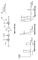
- Figure 1 depicts a chopping circuitry and amplifier 100, which is utilized as a component in many well-known circuits such as switched capacitor digital to analog converters.
- the input signal, x 1 (t) is modulated by chopper circuit 102 at a chopper control signal c(t) frequency of, f chop .
- Figure 2A depicts modulated input signal X 1 (f) in the frequency domain, centered on f chop, and harmonics of f chop .
- the amplitude of the modulated input signal X 1 (f) decreases with 1/n, where n is the harmonic number.
- the baseband of X 1 (f) extends to frequency f B , which in audio applications is about 20-25 kHz.
- the 1/f noise is added to the modulated input signal x 1 (t) after chopping.
- Figure 2B illustrates the 1/f noise in the frequency domain.
- the energy of the 1/f noise is primarily located within low frequencies, including the baseband of audio signals.
- Gain stage 104 which may be part of a larger circuit (not shown), such as a low pass filter, amplifies the modulated input signal x 1 (t) and 1/f noise.
- Chopper circuit 106 demodulates the output signal of gain stage 102 at the frequency of chopper signal c(t) to produce output signal x 2 (t).
- Figure 2C depicts signal x 2 (t) and the 1/f noise signal in the frequency domain.
- a low pass filter (not shown) attenuates signals having frequency components of x 2 (t) outside f B .
- Welland recognized that, in an ADC, choosing a chopping frequency equal to one-half of the sampling frequency of an analog input signal can actually increase the modulation of noise into an input signal's baseband. Thus, Welland selected a chopping frequency equal to the sampling frequency of the analog input signal.
- Welland included an analog modulator with at least one stage of amplification having a frequency response that provides a substantial amount of attenuation at the sampling frequency of the analog modulator in the Welland design. Thus, the amplification stage attenuates 1/f noise, which is shifted up in frequency by chopping to the sampling frequency.
- DACs are in many ways very different from ADCs. Consequently, chopping frequencies of DACs are selected for different reasons than ADCs.
- Conventional technologies implement chopping in DACs at a chopping frequency that is as low as possible relative to a digital sampling frequency.
- the DAC chopping frequency is conventionally chosen just high enough to shift 1/f noise out of the baseband of the input signal in order to minimize parasitic effects associated with chopping circuitry.
- a digital to analog converter system includes a digital to analog converter ("DAC") to (i) receive a digital input signal, sampled at frequency f s and having frequency components primarily within a frequency baseband, and out of baseband noise and to (ii) convert the digital input signal into a representative analog signal.
- the DAC includes a modulation circuit having a modulation frequency of approximately or equal to f s l2 to modulate the digital input signal by approximately or equal to f s l2 and a gain stage coupled to the modulation circuit to receive signals modulated by the modulation circuit and provide gain for the DAC, wherein during operation the gain stage is associated with noise having frequencies within the baseband.
- the DAC further includes a demodulation circuit, coupled to the gain stage and having a demodulation frequency equal to approximately or equal to f s /2, to demodulate signals and allow frequency components of the input signal to fold back into the baseband, to reduce fold back into the baseband of the quantization noise frequency components, and modulate the noise associated with the gain stage substantially out of the baseband.
- a demodulation circuit coupled to the gain stage and having a demodulation frequency equal to approximately or equal to f s /2, to demodulate signals and allow frequency components of the input signal to fold back into the baseband, to reduce fold back into the baseband of the quantization noise frequency components, and modulate the noise associated with the gain stage substantially out of the baseband.
- a method of converting a digital input signal, sampled at a frequency f s and having frequencies within a baseband, into a representative analog signal, modulating out of the baseband low frequency noise components associated with a digital to analog converter ("DAC") gain stage, and reducing fold back of quantization noise, frequency components residing outside the baseband includes modulating a DAC input signal, which is derived from the digital input signal and the quantization noise by a modulation frequency of approximately or equal to f S l2.
- the method further includes providing the modulated DAC input signal to the DAC gain stage.
- the method also includes demodulating output signals of the DAC gain stage by a demodulation frequency of approximately or equal to f S /2 to allow frequency components of the input signal to fold back into the baseband, to prevent fold back into the baseband of the quantization noise frequency components, and modulate the noise associated with the gain stage substantially out of the baseband.
- an audio system in another embodiment, includes a digital audio signal source.
- the audio system further includes a digital to analog converter (“DAC") to (i) receive a digital input signal from the digital audio signal source, sampled at frequency f S and having frequency components primarily within a frequency baseband, and out of baseband noise and to (ii) convert the digital input signal into a representative analog signal.
- the DAC includes a modulation circuit having a modulation frequency of approximately or equal to f S /2 to modulate the digital input signal by approximately or equal to f S /2 and a gain stage coupled to the modulation circuit to receive signals modulated by the modulation circuit and provide gain for the DAC, wherein during operation the gain stage is associated with noise having frequencies within the baseband.
- the DAC also includes a demodulation circuit, coupled to the gain stage and having a demodulation frequency equal to approximately or equal to f S /2, to demodulate signals and allow frequency components of the input signal to fold back into the baseband, to reduce fold back into the baseband of the quantization noise frequency components, and modulate the noise associated with the gain stage substantially out of the baseband.
- the audio system also includes an amplifier coupled to the DAC and an audio output device coupled to the DAC.
- Signal processing technology operates on analog, digital and mixed signals (analog and digital).
- audio signals representing a signal of interest and having frequency components residing within a baseband
- DAC digital-to-analog converter
- Audio frequency analog output signals produce sound through a loudspeaker, headphones, or other output device.
- Embodiments of the DAC system described herein utilize chopping modulation technology to remove 1/f and other baseband noise from a baseband of a signal of interest. In some embodiments, the chopping frequency is carefully selected to reduce noise fold back into the baseband.
- one or more notch filters are implemented to address parasitic modulation and associated noise fold back associated with non-ideal system properties, such as parasitic impedances.
- a notch filter reduces the fold back of the noise into the baseband from modulation at the chopping frequency and harmonic frequencies thereof.
- DAC digital to analog converter
- Chopping circuitry in general when combined with non-ideal (i.e. real-world) circuit components includes as a byproduct the fold back of noise frequency components into the baseband. Noise frequency components in a baseband of a signal of interest are generally undesirable. Chopping often results in the fold back of such noise into a baseband of a digital input signal due to modulation caused by non-ideal properties of the digital signal processing systems.
- a digital signal processing system that includes a DAC with chopping circuitry operating at a chopping frequency equal to or approximately equal to one-half of a digital input signal sampling frequency addresses noise fold back concerns due to parasitic modulation at twice the chopping frequency, 2 f chop . Chopping at one-half the sampling frequency results in fold back into the baseband of frequency components of the input signal itself, rather than noise components.
- a notch filter inserts zeros into the frequency response of the DAC at the chopping frequency and harmonics.
- the notch filter is preferably designed to have an attenuation band at least equal to the baseband of an input signal of interest.
- the notch filter also assists in preventing fold back of noise into a baseband of the input signal of noise modulated at f chop .
- the various chopping signals are also preferably coordinated to reduce the generation of additional noise within the system.
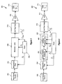
- FIG. 3 depicts digital signal processing system 300.
- Digital signal processing system 300 represents one embodiment of a system that benefits from setting a chopping frequency f chop equal to one-half a signal sampling fiequency, f S .
- digital signal processing system 300 is an audio system for receiving, processing, and providing audio output signals.
- Input signal source 302 provides a digital input signal from any signal source, such as a compact disk player, MP3 player, audio/video system, or other audio recording and/or playback device.
- An interpolation filter 304 performs oversampling functions in a well-known manner on the digital input signal received from the input signal source 302.
- the interpolation filter 304 has a sampling frequency, f S , provided by clock 308.
- the modulator - DAC 306 processes the interpolated digital input signal to convert the digital input signal into an analog signal.
- the modulator - DAC 306 also includes chopping circuitry to modulate noise, such as 1/f noise out of a baseband of the digital input signal.
- Clock 308 provides various control signals to modulator - DAC 306 as described below.
- clock 308 provides a clock signal having a frequency of f S to modulator - DAC 306 and provides various chopping signals that have a frequency f chop equal or approximately equal to f S /2.
- f chop f S /2 exactly.
- variations in timing are generally inevitable in real systems due to factors such as non-ideal components and parasitic impedances. To avoid repeating "approximately" throughout this description unless otherwise indicated, references to "equal" in the context of f chop equal f S / 2 mean “approximately equal or equal”.
- a low pass filter 310 generally having a corner frequency at or about the corner frequency, f B , of the baseband of the input signal, attenuates output signal frequency components outside the baseband.
- a filtered output signal from low pass filter 310 is generally amplified before being provided to load 314, especially when driving a low impedance load.
- amplifier 312 amplifies the filtered output signal and provides the signal to load 314.
- load 314 may be any load, in audio applications, load 314 represents, for example, loudspeakers, headphones, and other sound producing devices.
- Figure 4 depicts digital signal processing system 400, which is one embodiment of the digital signal processing system 300.
- the modulator-DAC 402 implements modulator - DAC 306 with a delta-sigma modulator 404 and a switched capacitor DAC 406.
- the delta-sigma modulator 404 provides a series of multi-bit output signals to switched capacitor DAC 406.
- the output signals of delta-sigma modulator 404 have an average value over a predetermined time equal to the digital input signal plus quantization error.
- “Delta-sigma modulator” and “sigma-delta modulator,” a commonly used term, are interchangeable terms for purposes of this specification.
- the delta-sigma modulator is clocked at f S .
- the frequency f S is selected based upon the particular application of digital signal processing system 400.
- frequency f S is, for example, 6.144 MHz, which reflects a 128 bit word representation of an audio signal originally sampled at 48 kHz.
- the frequency spectrum of the quantization noise generated by delta-sigma modulator 404 resides primarily outside of an audio frequency baseband, approximately 0 to 25 kHz.
- the quantization noise represents one example of noise that has frequency components that can fold back and mix with a signal of interest in the baseband when using conventional technology.
- FIG. 5 depicts a multibit, switched capacitor DAC 500, which is one embodiment of switched capacitor DAC 406. Any DAC could substitute for switched capacitor DAC 406.
- Switched capacitor DAC 500 includes modulating chopping circuitry 502, which modulates the input signal provided by delta-sigma modulator 404.
- Switched capacitor DAC 500 includes demodulating chopping circuitry 508, which demodulates the output signal of gain stage G1.
- capacitor banks 504 and 506 each contain an identical number of "N" parallel coupled, corresponding sampling capacitors, collectively referred to as Cs+ (504) and C s . (506). Each sampling capacitor in capacitor bank 504 is charged in accordance with one-bit of each N-bit word in the delta sigma modulator 404 output signal. The same charging scheme applies to capacitor bank 506. Capacitors associated with the same bit within capacitor banks 504 and 506 are referred to herein as "corresponding capacitors”.
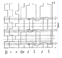
- the switched capacitor DAC 500 operates in accordance with the control signals depicted in Figure 6 .
- all of the control signals are generated with reference to an analog clock signal.
- the control signals including chopping circuitry control signals, are preferably phase-shifted relative to the analog clock signal and relative to each other to allow settling of components and to minimize the inclusion of switching noise into the signal being processed. Settling time is dependent upon specific component value and other design considerations well-known to those of ordinary skill in the art. As will be described in more detail below, it has been identified that while the inclusion of chopping circuitry 502 and 508 addresses some low frequency noise concerns (e.g.
- switched capacitor DAC 500 begins at time t0, after the analog clock rises and a sufficient time has been allocated to allow circuits to settle, control signal ⁇ 1 rises for a sufficient time to cause switches 510 and 512 to conduct and short one plate of Cs+ 504 and Cs- 506 sampling capacitors to the common mode voltage Vcm.
- the sampling capacitors Cs+ 504 and Cs- 506 are charged to Vdd through respective switches 518 and 522 or discharged to ground GND, in accordance with the value of d* and d * associated with each sampling capacitor, through respective switches 520 and 524 while control signal ⁇ 1 is HIGH.
- Each value of d represents the ith bit of the N-bit output word, and d represents the complement of d, 0 ⁇ i ⁇ N-1, where N is the number of bits in an output word of delta sigma modulator 404.
- Each of switches 518, 520, 522, and 524 represent N respective switches, one for each of the N bits in the delta sigma modulator 404 N-bit output word, where N is, for example, 16.
- control signal ⁇ 2 causes switches 526, 528, 530 and 532 to conduct and transfer charge to integrating capacitors C I + 514 and C I - 516.
- Chopping circuitry 502 modulates the DAC input signal at input terminals 534 and 536 and chopping circuitry 508 demodulates the output signal of gain stage G1.
- Table 2 Chopping Circuitry Chopping Circuitry Operational Phase Chopping Circuitry 502 Modulation Chopping Circuitry 508 Demodulation
- Chopping modulation and demodulation circuitry use direct and cross-over switches to modulate low frequency noise, such as 1/f noise, out of a signal baseband. Chopping circuits are particularly useful with low frequency baseband applications such as audio applications.
- the direct switches coupled to respective input and output terminals of a differential amplifier have nonoverlapping conduction phases with cross-over switches coupled to the terminals of the differential amplifier. Additionally, the direct switches coupled to the respective input and output terminals have different duty cycles with respect to each other, and the cross-over switches coupled to the respective input and output terminals of the differential amplifier have different duty cycles with respect to each other to reduce noise transfer to an output of the system.
- control signals ⁇ chA and ⁇ chB of chopping circuitry 502 are non-overlapping to prevent signal corruption, preferably square waves (or approximations thereto), and control conduction of switches 538 and 540, respectively.
- Chopping circuitry 508 control signals ⁇ chC and ⁇ chD are also non-overlapping to prevent signal corruption, preferably square waves (or approximations thereto), and control conduction of switches 542 and 544, respectively.
- a rise of control signal ⁇ chA at time t 3 causes direct switches 538 to conduct and pass-through the delta-sigma modulated input signal at input terminals 534 and 536 straight to gain stage G1 during the first depicted Dump phase occurring from t 4 to t 5 .
- Direct switches 542 also conduct at time t 3 , and, during the first Dump phase, gain stage G1 passes through an amplified output signal straight to the input terminals of gain stage G2.
- Control signal ⁇ chC falls at t 6 followed by the fall of ⁇ chA at t 7 .
- the delay between turning direct switches 542 "off" (nonconducting) and turning direct switches 538 off at the input of gain stage G1 is set by control signals ⁇ chC and ⁇ chA to provide a delay sufficient to prevent the switching noise associated with switches 538 from being passed through to the outputs V o + and V o -.
- the delay time depends on the particular implementation of the DAC and chopping circuitry. In one embodiment the delay is on the order of 5 ns. Conduction and nonconduction of switches 538, 540, 542, and 544 controlled by the edge of control signals or controlled by other properties of the control signals in a well-known manner.
- a rise of cross-over control signals ⁇ chB following the fall of ⁇ chA causes cross-over switches 540 to conduct.
- the delta-sigma modulated input signal at input terminals 534 and 536 cross-over to opposite inputs of gain stage G1 during the second Dump phase.
- Control signal ⁇ chD falls at t 11 followed by the fall of ⁇ chB at t 12 again with a delay sufficient to prevent the switching noise associated with switches 540 from being passed through to the outputs V o + and V o -.
- control signal ⁇ chA rises again, and the processes described above occurring between t 3 and t 12 repeat during operation of switched capacitor DAC 500.
- the timing of control signals ⁇ chA, ⁇ chB , ⁇ chC , and ⁇ chD are achieved, in one embodiment, by using the chop clock reference signal as a reference and using delay elements to achieve the desired timing.
- V o +" and V o - represent the respective differential output signals of switched capacitor DAC 500.
- Gain stages G1 and G2 are dual output, fully differential operational amplifiers, which can be of any design suitable for the application to which they are applied. Other gain stage implementations may be used. Other embodiments of switched capacitor DAC 500 use a single gain stage or more than two gain stages.
- DACs often contain non-ideal properties such as parasitic capacitances or timing errors. Such non-ideal properties can produce parasitic modulation, which can corrupt a signal of interest due to, for example, fold back of noise into the baseband and mixing with the signal of interest.
- the chopping circuitry 502 and 508 in association with various parasitic capacitances as well as other non-ideal properties can cause noise to occur at f chop 2 f chop , and odd harmonics of f chop and 2f chop .
- parasitic capacitors C 2p+ and C 2p- cause continuous time glitches to occur at the output of switched capacitor DAC 500 at a frequency of 2 f chop .
- notch filters are added at parasitic modulation frequencies to attenuate signals folded back into the baseband by parasitic modulation at f chop .
- Gain stage G2 also introduces 1/f noise. However, if the gain of gain stage G1 is relatively high, the energy level of the gain stage G2 1/f noise is relatively low.
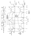
- Figure 7 depicts the frequency response of switched capacitor DAC 500 and low pass filter 310 at various points of reference.
- the frequency axis and amplitudes are not to scale, and the depiction of switched capacitor DAC 500 has been simplified to highlight points of reference in the frequency domain.
- Figure 7 only depicts positive frequencies, and harmonics are not shown but are affected in the same way as their fundamental frequencies. It is understood that a mirror image of the frequency spectrums in Figures 7 and 13 reside at negative frequencies.
- the baseband of the input signal of interest from input signal source 302 has a bandwidth ranging from 0 Hz to f B , where f B is about 25 kHz.
- frequency components of the input signal 702 from the input signal source 302 reside within the baseband, and frequency components of the quantization noise 704 from delta sigma modulator 404 reside between frequencies f B and f S minus f B .
- the DAC input signal 706, received at input terminals 534 and 536, includes the input signal 702 and quantization noise 704.
- the spectrum is repeated at f S and integer multiples of f S in accordance with digital sampling theory.
- chopping circuit 502 modulates the DAC input signal 706 at reference point A by frequency f chop , thereby transposing the frequency spectrum at reference point A up by frequency f chop .
- the delta-sigma modulated input signal 702 now resides within frequencies f chop +/- f B with a mirror image between f chop -f B and f chop , and some quantization noise 704 resides within the baseband.
- the 1/f noise 708, with higher energy levels in the baseband, is introduced and shown at reference point C.
- Chopping circuit 508 demodulates the signal at reference point C, thereby transposing the frequency spectrum down by f chop as depicted at reference point D.
- the modulated input signal 702 (the signal of interest) is transposed back to the baseband.
- the 1/f noise is modulated by f chop , thereby transposing the 1/f noise frequency components up by f chop as depicted at reference point D.
- parasitic modulation causes fold back into the baseband of signals having frequencies within frequencies 2 f chop +/- f B .
- the signal of interest resides at f S +/- f B .
- the signal of interest 702 is folded back and mixed with itself.
- the low pass filter 310 attenuates frequency components in the output of gain stage G2 as depicted at reference point E.
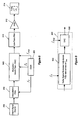
- modulator-notch filter-DAC 800 represents an embodiment of modulator - DAC 306 having a notch filter to attenuate frequency components within f chop +/- f B prior to chopping.
- fold back of noise signals within frequencies f chop +/- f B into the baseband is reduced in direct relation to the attenuation of noise within frequencies f chop +/- f B .
- the notch filter of modulator-notch filter-DAC 800 is implemented within the digital signal processing system 400.
- the delta-sigma modulator 1000 includes a conventional summing node 1002 to sum a received input signal and the negative of the quantizer feedback output signal 1012.
- the delta-sigma modulator 1000 also includes a first order main loop filter H(z) 1004 for noise shaping.
- the main loop filter H(z) 1004 is modified by adding a parallel notch loop filter 1008.
- the notch loop filter 1008 has transfer functions z -1 /(1 + z -1 ) with gain al and notch characteristics and 1/(1 + z -1 ) with gain a2. Coefficients of the notch filter 1008 and gain are dependent on the specific application of digital signal processing system 300 and are determined in a well-known manner to provide attenuation of frequency components within frequencies f chop +/- f B and harmonics.
- Figure 11 depicts another embodiment of modulator-notch filter-DAC 800 that includes a notch FIR filter 1102 implemented as a 2-tap FIR boxcar filter.
- Coefficients of notch FIR filter 1102 are also dependent on the specific application of digital signal processing system 300 and are determined in a well-known manner to provide attenuation of frequency components within frequencies f chop +/- f B and harmonics. It will be recognized by those of ordinary skill in the art that other notch filter embodiments can be used to achieve attenuation at frequencies f chop +/- f B and harmonics thereof, and, thus, prevent noise otherwise present at f chop +/- f B and harmonics thereof from folding into the baseband and mixing with the signal of interest.
- the frequency and amplitude axes are not to scale, and the depiction of switched capacitor DAC 500 has been simplified to highlight points of reference in the frequency domain. Also, for clarity Figure 13 only depicts positive frequencies, and harmonics are not shown but are affected in the same away as their fundamental frequencies.
- the baseband of the input signal of interest from input signal source 302 has a bandwidth ranging from 0 Hz to f B , where f B is about 25 kHz.
- Figure 13 depicts the effects of parasitic fold back of noise at frequency f chop , with and without an attenuation band centered at f chop .
- Chopping events at reference points A, B, C, and E occur as previously described with respect to Figure 7 .
- nonideal properties associated with DACs such as switched capacitor DAC 500, can result in parasitic modulation at the chopping frequency f chop and harmonics and at 2 f chop and harmonics.
- the parasitic modulation at frequencies f chop and 2 f chop cause signals having frequencies within f chop + / - f B and 2 f chop +/ -f B to fold into the baseband and mix with the signal of interest 702.
- the frequency spectrum 1302 illustrates the fold back of quantization noise 704 into the baseband in the absence of signal attenuation at frequencies within f chop +/- f B .
- the folded back quantization noise mixes with the signal of interest 702 and, thus, corrupts the signal of interest 702.
- the frequency spectrum 1304 illustrates the attenuation of quantization noise 704 within frequencies f chop +/- f B due to the presence of a notch filter, such as notch loop filter 1008 or notch FIR filter 1102.
- the attenuation of noise within frequencies f chop +/- f B reduces or prevents, depending on the degree of attenuation and attenuation bandwidth, fold back of noise due to parasitic modulation at frequency f chop .
- Notches can also be set at harmonics of f chop to prevent fold back of noise into the baseband.
- notch filters can be used to attenuate noise prior to chopping at any other parasitic modulation frequency or frequencies to prevent fold back of noise into the baseband during chopping.
- the signal processing system herein provides significant noise attenuation within a baseband of interest using carefully selected chopping frequencies and/or notch filters with attenuation bands around parasitic modulation frequencies.
- the signal processing systems disclosed herein can be manufactured using well-known integrated, discrete, or a combination of integrated and discrete components. Additionally software in combination with a processor can be used to implement features of the signal processing systems, such as a notch filter.
- a notch filter Those of ordinary skill in the art will recognize that the signal processing systems disclosed herein can be implemented with a wide range of components other than those disclosed herein.
- the digital signal modulators could be implemented using mixed signal (analog and digital) technology.
- the attenuation bands of notch filters can be set to greater than, less than, or equal to f B depending on, for example, the amount of acceptable noise fold back into the baseband.
- the DAC many implementations of the DAC are possible including using a single bit delta-sigma modulator in place of the multi-bit delta-sigma modulator.
- the multi-bit switched capacitor circuit can remain a multi-bit circuit with an accumulation of bits from the single bit delta-sigma modulator or could be a single bit circuit.
Landscapes
- Engineering & Computer Science (AREA)
- Power Engineering (AREA)
- Theoretical Computer Science (AREA)
- Compression, Expansion, Code Conversion, And Decoders (AREA)
- Analogue/Digital Conversion (AREA)
- Amplifiers (AREA)
Claims (27)
- System, welches Folgendes umfasst:einen Digital-Analog-Konverter ("DAC"), um (i) ein digitales Eingangssignal zu empfangen, welches bei einer Frequenz fS abgetastet ist und Frequenzkomponenten hauptsächlich innerhalb eines Frequenzbasisbandes und Rauschen außerhalb des Basisbandes aufweist, und um (ii) das digitale Eingangssignal in ein darstellenden Analogsignal zu konvertieren, wobei der DAC Folgendes umfasst:eine Modulationsschaltung (502) mit einer Modulationsfrequenz von etwa oder gleich fS /2, um das digitale Eingangssignal mit etwa oder gleich fS /2 zu modulieren;eine Verstärkungsstufe, die mit der Modulationsschaltung gekoppelt ist, um durch die Modulationsschaltung modulierte Signale zu empfangen und eine Verstärkung für den DAC vorzusehen, wobei die Verstärkungsstufe im Betrieb mit einem Rauschen verknüpft ist, welches Frequenzen innerhalb des Basisbandes aufweist; undeine Demodulationsschaltung (508), die mit der Verstärkungsstufe gekoppelt ist und eine Demodulationsfrequenz besitzt, die etwa gleich oder gleich zu fS /2 ist, um Signale zu demodulieren und zu ermöglichen, Frequenzkomponenten des Eingangssignals in das Basisband zurückzufalten, um ein Zurückfalten der quantisierten Rauschfrequenzkomponenten in das Basisband zu reduzieren, und um das mit der Verstärkungsstufe verknüpfte Rauschen im Wesentlichen außerhalb des Basisbandes zu modulieren.
- System nach Anspruch 1, welches weiterhin Folgendes umfasst:einen Modulator (404), der mit dem DAC gekoppelt ist, um ein erstes digitales Ausgangssignal zu empfangen, welches mit einer Frequenz fS abgetastet ist, um das digitale Eingangssignal zu modulieren, wobei das erste digitale Eingangssignal Frequenzkomponenten umfasst, die innerhalb des Basisbandes liegen, welches von den Frequnzen f1 und f2 begrenzt ist, und wobei ein Nebenprodukt der ersten digitalen Eingangssignalmodulation ein Quantisierungsrauschen aufweist mit Frequenzkomponenten, die außerhalb des Basisbandes liegen, wobei das Eingangssignal des DAC von dem modulierten ersten digitalen Eingangssignal erlangt wird.
- System nach Anspruch 2, wobei f1 und f2 jeweils niedrige und hohe Frequenzen eines Audiosignalbasisbandes definieren.
- System nach Anspruch 3, wobei f1 etwa oder gleich 0 Hz ist und f2 etwa gleich 25 kHz ist.
- System nach Anspruch 2, wobei der Modulator (404) ein Delta-Sigma-Modulator ist und das System ferner Folgendes umfasst:einen Kerbfilter, der in einer Rückkopplungsschleife des Modulators implementiert ist und ein Frequenzdämpfungsband aufweist, um Signale mit Frequenzen innerhalb eines Bandes zu dämpfen, welches in das Basisband durch paraistäre Modulation zurückgefaltet wird.
- System nach Anspruch 5, wobei das Frequenzdämpfungsband +/- eine Bandbreite des Frequenzbasisbands ist.
- System nach Anspruch 5, wobei das Frequenzdämpfungsband um fSl2 zentriert ist.
- System nach Anspruch 1, wobei die Modulationsschaltung (502) ein Zerhackermodulator ist, der Serien- und Überkreuzschalter (538, 540) umfasst, um Eingangssignale der Verstärkungsstufe zu zerhacken, wobei die Demodulationsschaltung (508) eine Zerhackerschaltung ist, die Serien- und Überkreuzschalter (542, 544) umfasst, um Ausgangssignale der Verstärkungsstufe zu zerhacken, und wobei die Verstärkerstufe eine Komponente eines vollständigen Differentialverstärkers ist.
- System nach Anspruch 1, wobei der DAC einen geschaltenen, kapazitiven Digital-Analog-Konverter (406) umfasst.
- System nach Anspruch 9, wobei der geschaltete, kapazitive Digital-Analog-Konverter (406) Abtastungskondesatoren, um Ladung zu empfangen, die das Eingangssignal darstellt, einen Rückkopplungskondensator und Schalter zum Austausch von Ladung zwischen den Abtastungskondensatoren und dem Rückkopplungskondensator umfasst.
- System nach Anspruch 1, wobei das digitale Eingangssignal Audiofrequenzkomponenten aufweist.
- System nach Anspruch 1, das ferner Folgendes umfasst:einen Kerbfilter, um das modulierte digitale Eingangssignal zu empfangen und ein gefiltertes Ausgabesignal zu dem DAC zu liefern, wobei der Kerbfilter ein Frequenzdämpfungsband aufweist, um Signale mit Frequenzen innerhalb eines Bandes zu dämpfen, welche in das Basisband durch parasitäre Modulation zurückgefaltet werden.
- System nach Anspruch 12, wobei das Frequenzdämpfungsband +/- eine Bandbreite des Frequenzbasisbandes ist und um fS /2 zentriert ist.
- System nach Anspruch 12, wobei der Filter ein digitaler Finite-Impule-Response-Filter ist, der unter Verwendung von Hardwarekomponenten implementiert ist.
- System nach Anspruch 1,
wobei die Modulationsschaltung (502) weiterhin Folgendes umfasst:Eingangsanschlüsse, um das digitale Eingangssignal zu empfangen; undDirekt- und Überkreuzschalter (538, 540), die gekoppelt sind, um ein Differentialeingangssignal abwechselnd durchzuleiten oder zu überkreuzen gemäß einem Durchleitungssteuersignal ΦchA und einem Überkreuzsteuersignal ΦchB,wobei das Steuersignal ΦchA gegenphasig zum Steuersignal ΦchB ist; und wobei die Demodulationsschaltung (508) weiterhin Folgendes umfasst:Eingangsanschlüsse, um ein Ausgangssignal der Verstärkungsstufe zu empfangen und das Differentialeingangssignal, welches von der Modulationsschaltung moduliert wird, abwechselnd durchzuleiten und zu überkreuzen gemäß einem Durchleitungssteuersignal ΦchC und einem Überkreuzsteuersignal ΦchD, wobei das Steuersignal ΦchD gegenphasig zu ΦchB ist, und das Steuersignal ΦchA und ΦchC mit den Signalen ΦchB und ΦchD nicht überlappen. - System nach Anspruch 15, wobei das Steuersignal ΦchC dafür eingerichtet ist, die Direktschalter (524), die von ΦchC gesteuert werden, zu veranlassen, nicht leitfähig vor einer Nichtleitfähigkeit der Direktschalter (538), die von ΦchA gesteuert werden, zu werden, und ΦchD dafür eingerichtet ist, die Direktschalter (544), die von ΦchD gesteuert werden, zu veranlassen, nicht leitfähig vor einer Nichtleitfähigkeit der Direktschalter (540), die von ΦchB gesteuert werden, zu werden.
- System nach Anspruch 15, wobei die Steuersignale ΦchA, ΦchB, ΦchC und ΦchD Rechteckwellen sind.
- Verfahren zum Konvertieren eines digitalen Eingangssignals, welches bei einer Frequenz fS abgetastet ist und Frequenzen innerhalb eines Basisbandes aufweist, in ein darstellendes Analogsignal, zum Modulieren von niedrigen Frequenzrauschkomponenten außerhalb des Basisbandes, welche mit einer Digital-Analog-Konverter (DAC)-Verstärkerstufe verknüpft sind, und zum Reduzieren von einer Rückfaltung von Quantisierungsrauschfrequenzkomponenten, welche außerhalb des Basisbandes liegen, wobei das Verfahren Folgendes umfasst:Modulieren eines DAC-Eingangssignals, welches von einem digitalen Eingangssignal erlangt wird, und das Quantifizierungsrauschen durch eine Modulationsfrequenz von etwa oder gleich fS /2;Liefern des modulierten DAC-Eingangssignals an die DAC-Verstärkungsstufe; undDemodulieren von Ausgangssignalen der DAC-Verstärkungsstufe durch eine Demodulationsfreuqenz von etwa oder gleich fSl2, um ein Zurückfalten von Frequenzkomponenten des Eingangssignals in das Basisband zu ermöglichen, um ein Zurückfalten der Quantisierungsrauschfrequenzkomponenten in das Basisband zu reduzieren, und das Rauschen, welches mit der Verstärkerstufe verknüpft ist, im Wesentlichen außerhalb des Basisbandes zu modulieren.
- Verfahren nach Anspruch 18, wobei das Modulieren des DAC-Eingangssignals ein Rauschsignal mit Frequenzkomponenten erzeugt, welche um fS /2 zentriert sind, wobei das Verfahren weiterhin Folgendes umfasst:Filtern des modulierten digitalen Eingangssignals, um Rauschsignalkomponenten mit einer Frequenz bei fS /2 +/- fB zu dämpfen, wobei fB eine Eckfrequenz der Bandbreite des Basisbandes ist.
- Verfahren nach Anspruch 19, wobei das Filtern des modulierten digitalen Signals weiterhin Folgendes umfasst:Filtern des digitalen Eingangssignals unter Verwendung eines digitalen Finite-Input-Response-Kerbfilters.
- Verfahren nach Anspruch 18, das weiterhin Folgendes umfasst:Modulieren des digitalen Eingangssignals, welches das Quantisierungsrauschen als ein Nebenprodukt des Modulieren des Eingangssignals erzeugt.
- Verfahren nach Anspruch 21, wobei das Modulieren des DAC-Eingangssignals ein Rauschsignal mit Frequenzkomponenten, welche um fS /2 zentriert sind, erzeugt, und das Verfahren weiterhin Folgendes umfasst:Modulieren des digitalen Eingangssignals, welches ein Modulieren des digitalen Eingangssignals unter Verwendung eines Delta-Sigma-Modulators (404) umfasst, undFiltern des modulierten digitalen Eingangssignals, um Signalkomponenten mit Frequenzen um etwa fS /2 +/- fB zu dämpfen, wobei fB eine Eckfrequenz einer Bandbreite des Basisbandes ist, wobei das Filtern des modulierten digitalen Signals ferner ein Filtern des modulierten digitalen Eingangssignals innerhalb einer Rückkopplungsschleife des Delta-Sigma-Modulators (404) umfasst.
- Verfahren nach Anspruch 18, wobei das digitale Eingangssignal ein Audiosignal ist.
- Verfahren nach Anspruch 18, wobei:das Modulieren des DAC-Eingangssignals weiterhin Folgendes umfasst: Abwechselndes Durchleiten und Überkreuzen des DAC-Eingangssignals gemäß einem Durchgangssteuersignal ΦchA und einem Überkrezungssteuersignal ΦchB, wobei das Steuersignal ΦchA gegenphasig zum Steuersignal ΦchB ist; unddas Demodulieren der Ausgangssignale der DAC-Verstärkerstufe weiterhin Folgendes umfasst: Abwechselndes Durchleiten und Überkreuzen des DAC-Eingangssignals, welches durch die Modulationsschaltung moduliert ist, gemäß Durchleitungssteuersignalen ΦchC und einem Überkreuzungssteuersignal ΦchD, wobei das Steuersignal ΦchD gegenphasig zu ΦchB ist, und die Steuersignale ΦchA und ΦchC mit den Steuersignalen ΦchB und ΦchD nicht überlappen.
- Verfahren nach Anspruch 24, das weiterhin Folgendes umfasst:Beenden des Durchleitens des DAC-Eingangssignals gemäß einem Steuersignal ΦchC vor einem Beenden des Durchleitens des DAC-Eingangssignals gemäß dem Steuersignal ΦchA; undBeenden des Überkreuzens des DAC-Eingangssignals gemäß dem Steuersignal ΦchD vor einem Beenden des Überkreuzens des DAC-Eingangssignals gemäß dem Steuersignal ΦchB.
- System nach Anspruch 1, das weiterhin Folgendes umfasst:eine digitale Audiosignalquelle;einen Verstärker, der mit dem DAC gekoppelt; undeine Audioausgabevorrichtung, die mit dem DAC gekoppelt ist.
- System nach Anspruch 26, wobei die Modulationsschaltung (502) ein Zerhackermodulator ist, der Serien- und Überkreuzungsschalter (538, 540) umfasst, um Eingangssignale der Verstärkerstufe zu zerhacken, die Demodulationsschaltung (508) eine Zerhackerschaltung ist, welche Serien- und Überkrezungsschalter (542, 544) umfasst, um Ausgangssignale der Verstärkerstufe zu zerhacken, und die Verstärkerstufe eine Komponente eines vollständigen Differentialverstärkers ist.
Applications Claiming Priority (5)
| Application Number | Priority Date | Filing Date | Title |
|---|---|---|---|
| US44129603P | 2003-01-21 | 2003-01-21 | |
| US441296P | 2003-01-21 | ||
| US425285 | 2003-04-29 | ||
| US10/425,285 US6842486B2 (en) | 2003-01-21 | 2003-04-29 | Signal processing system with baseband noise modulation and noise fold back reduction |
| PCT/US2004/001514 WO2004066540A2 (en) | 2003-01-21 | 2004-01-21 | Signal processing system with baseband noise modulation and noise fold back reduction |
Publications (3)
| Publication Number | Publication Date |
|---|---|
| EP1590905A2 EP1590905A2 (de) | 2005-11-02 |
| EP1590905A4 EP1590905A4 (de) | 2011-01-12 |
| EP1590905B1 true EP1590905B1 (de) | 2012-11-28 |
Family
ID=32717562
Family Applications (1)
| Application Number | Title | Priority Date | Filing Date |
|---|---|---|---|
| EP04704054A Expired - Lifetime EP1590905B1 (de) | 2003-01-21 | 2004-01-21 | Signalverarbeitungssystem mit basisbandrauschmodulation und rauschrückfaltungsreduktion |
Country Status (4)
| Country | Link |
|---|---|
| US (1) | US6842486B2 (de) |
| EP (1) | EP1590905B1 (de) |
| JP (1) | JP2006516377A (de) |
| WO (1) | WO2004066540A2 (de) |
Families Citing this family (45)
| Publication number | Priority date | Publication date | Assignee | Title |
|---|---|---|---|---|
| US7084798B2 (en) * | 2004-01-16 | 2006-08-01 | Cirrus Logic, Inc. | Look-ahead delta sigma modulators with quantizer input approximations |
| US7170434B2 (en) * | 2004-01-16 | 2007-01-30 | Cirrus Logic, Inc. | Look-ahead delta sigma modulator with quantization using natural and pattern loop filter responses |
| US7187312B2 (en) * | 2004-01-16 | 2007-03-06 | Cirrus Logic, Inc. | Look-ahead delta sigma modulator having an infinite impulse response filter with multiple look-ahead outputs |
| US7009543B2 (en) * | 2004-01-16 | 2006-03-07 | Cirrus Logic, Inc. | Multiple non-monotonic quantizer regions for noise shaping |
| US7196647B2 (en) * | 2004-01-16 | 2007-03-27 | Cirrus Logic, Inc. | Signal processing with look-ahead modulator noise quantization minimization |
| US7148830B2 (en) * | 2004-01-26 | 2006-12-12 | Cirrus Logic, Inc. | Look-ahead delta sigma modulator with pruning of output candidate vectors using quantization error minimization pruning techniques |
| US7138934B2 (en) * | 2004-01-26 | 2006-11-21 | Cirrus Logic, Inc. | Pattern biasing for look-ahead delta sigma modulators |
| US7081843B2 (en) * | 2004-07-19 | 2006-07-25 | Cirrus Logic, Inc. | Overload protection for look-ahead delta sigma modulators |
| US7525365B1 (en) * | 2005-05-09 | 2009-04-28 | National Semiconductor Corporation | System and method for providing an offset voltage minimization circuit |
| US7183957B1 (en) * | 2005-12-30 | 2007-02-27 | Cirrus Logic, Inc. | Signal processing system with analog-to-digital converter using delta-sigma modulation having an internal stabilizer loop |
| US7391257B1 (en) | 2007-01-31 | 2008-06-24 | Medtronic, Inc. | Chopper-stabilized instrumentation amplifier for impedance measurement |
| US9615744B2 (en) | 2007-01-31 | 2017-04-11 | Medtronic, Inc. | Chopper-stabilized instrumentation amplifier for impedance measurement |
| US8265769B2 (en) * | 2007-01-31 | 2012-09-11 | Medtronic, Inc. | Chopper-stabilized instrumentation amplifier for wireless telemetry |
| US7385443B1 (en) * | 2007-01-31 | 2008-06-10 | Medtronic, Inc. | Chopper-stabilized instrumentation amplifier |
| US20080219331A1 (en) * | 2007-03-07 | 2008-09-11 | Matsushita Electric Industrial Co., Ltd. | Methods and apparatus for reducing the effects of DAC images in radio frequency transceivers |
| US9788750B2 (en) * | 2007-04-30 | 2017-10-17 | Medtronic, Inc. | Seizure prediction |
| US8781595B2 (en) | 2007-04-30 | 2014-07-15 | Medtronic, Inc. | Chopper mixer telemetry circuit |
| US8594779B2 (en) * | 2007-04-30 | 2013-11-26 | Medtronic, Inc. | Seizure prediction |
| US7554473B2 (en) * | 2007-05-02 | 2009-06-30 | Cirrus Logic, Inc. | Control system using a nonlinear delta-sigma modulator with nonlinear process modeling |
| US7894561B1 (en) | 2007-06-21 | 2011-02-22 | National Semiconductor Corporation | Method and system for providing dynamic DC offset correction |
| US7714757B2 (en) * | 2007-09-26 | 2010-05-11 | Medtronic, Inc. | Chopper-stabilized analog-to-digital converter |
| US20090082691A1 (en) * | 2007-09-26 | 2009-03-26 | Medtronic, Inc. | Frequency selective monitoring of physiological signals |
| US7623053B2 (en) * | 2007-09-26 | 2009-11-24 | Medtronic, Inc. | Implantable medical device with low power delta-sigma analog-to-digital converter |
| US8380314B2 (en) | 2007-09-26 | 2013-02-19 | Medtronic, Inc. | Patient directed therapy control |
| US8121694B2 (en) | 2007-10-16 | 2012-02-21 | Medtronic, Inc. | Therapy control based on a patient movement state |
| CN101925377A (zh) | 2008-01-25 | 2010-12-22 | 麦德托尼克公司 | 睡眠阶段的检测 |
| US9425747B2 (en) * | 2008-03-03 | 2016-08-23 | Qualcomm Incorporated | System and method of reducing power consumption for audio playback |
| JP2009232425A (ja) * | 2008-03-25 | 2009-10-08 | Toshiba Corp | 送信機 |
| US20100113964A1 (en) * | 2008-10-31 | 2010-05-06 | Wahlstrand John D | Determining intercardiac impedance |
| US8478402B2 (en) * | 2008-10-31 | 2013-07-02 | Medtronic, Inc. | Determining intercardiac impedance |
| US8189802B2 (en) * | 2009-03-19 | 2012-05-29 | Qualcomm Incorporated | Digital filtering in a Class D amplifier system to reduce noise fold over |
| US9770204B2 (en) | 2009-11-11 | 2017-09-26 | Medtronic, Inc. | Deep brain stimulation for sleep and movement disorders |
| US8072262B1 (en) * | 2010-06-28 | 2011-12-06 | Texas Instruments Incorporated | Low input bias current chopping switch circuit and method |
| KR101749958B1 (ko) * | 2010-07-08 | 2017-06-22 | 마이크로칩 테크놀로지 인코포레이티드 | 초퍼 기준 전압을 이용한 스위치형 커패시터 시그마-델타 변조기의 2단계 이득 교정과 스케일링 방식 |
| US8847139B2 (en) | 2010-08-24 | 2014-09-30 | Intersil Americas LLC | Methods, sub-systems and systems that reduce a mismatch error associated with an analog circuit |
| US8717211B2 (en) | 2010-11-30 | 2014-05-06 | Qualcomm Incorporated | Adaptive gain adjustment system |
| US9521979B2 (en) | 2013-03-15 | 2016-12-20 | Medtronic, Inc. | Control of spectral agressors in a physiological signal monitoring device |
| US9439150B2 (en) | 2013-03-15 | 2016-09-06 | Medtronic, Inc. | Control of spectral agressors in a physiological signal montoring device |
| US9344045B2 (en) * | 2013-05-29 | 2016-05-17 | Intel Mobile Communications GmbH | Amplifier and method of amplifying a differential signal |
| US9924904B2 (en) | 2014-09-02 | 2018-03-27 | Medtronic, Inc. | Power-efficient chopper amplifier |
| US10341148B2 (en) * | 2017-08-25 | 2019-07-02 | Mediatek Inc. | Sigma-delta modulator and associated system improving spectrum efficiency of wired interconnection |
| CN109286378B (zh) * | 2018-09-26 | 2022-04-12 | 复旦大学 | 一种具有自适应失调调节功能的斩波电路 |
| US11251802B1 (en) * | 2020-08-03 | 2022-02-15 | xMEMS Labs, Inc. | Nonlinear digital-to-analog converter |
| US11271480B2 (en) | 2020-08-03 | 2022-03-08 | xMEMS Labs, Inc. | Driving circuit with energy recycle capability and method thereof |
| JP2022148473A (ja) * | 2021-03-24 | 2022-10-06 | 株式会社ミツトヨ | フロントエンド回路及びエンコーダ |
Family Cites Families (6)
| Publication number | Priority date | Publication date | Assignee | Title |
|---|---|---|---|---|
| US4138649A (en) | 1977-03-25 | 1979-02-06 | Emerson Electric Co. | Amplifier system |
| US4939516B1 (en) | 1988-06-13 | 1993-10-26 | Crystal Semiconductor Corporation | Chopper stabilized delta-sigma analog-to-digital converter |
| US5039989A (en) | 1989-10-27 | 1991-08-13 | Crystal Semiconductor Corporation | Delta-sigma analog-to-digital converter with chopper stabilization at the sampling frequency |
| US5148167A (en) * | 1990-04-06 | 1992-09-15 | General Electric Company | Sigma-delta oversampled analog-to-digital converter network with chopper stabilization |
| US5561660A (en) * | 1995-04-05 | 1996-10-01 | Silicon Systems, Inc. | Offset and phase correction for delta-sigma modulators |
| US6744392B2 (en) * | 2002-08-02 | 2004-06-01 | Cirrus Logic, Inc. | Noise shapers with shared and independent filters and multiple quantizers and data converters and methods using the same |
-
2003
- 2003-04-29 US US10/425,285 patent/US6842486B2/en not_active Expired - Lifetime
-
2004
- 2004-01-21 WO PCT/US2004/001514 patent/WO2004066540A2/en not_active Ceased
- 2004-01-21 EP EP04704054A patent/EP1590905B1/de not_active Expired - Lifetime
- 2004-01-21 JP JP2006501064A patent/JP2006516377A/ja active Pending
Also Published As
| Publication number | Publication date |
|---|---|
| EP1590905A4 (de) | 2011-01-12 |
| WO2004066540A2 (en) | 2004-08-05 |
| US20040141558A1 (en) | 2004-07-22 |
| JP2006516377A (ja) | 2006-06-29 |
| US6842486B2 (en) | 2005-01-11 |
| WO2004066540A3 (en) | 2004-11-11 |
| EP1590905A2 (de) | 2005-11-02 |
Similar Documents
| Publication | Publication Date | Title |
|---|---|---|
| EP1590905B1 (de) | Signalverarbeitungssystem mit basisbandrauschmodulation und rauschrückfaltungsreduktion | |
| EP1590888B1 (de) | Signalverarbeitungssystem mit basisbandrauschmodulation und rauschfilterung | |
| EP1590934B1 (de) | Signalverarbeitungssystem mit basisbandrauschen-modulations-chopper-schaltungs-timing zur rauschverringerung | |
| US8570200B2 (en) | Continuous-time oversampled converter having enhanced immunity to noise | |
| US4939516A (en) | Chopper stabilized delta-sigma analog-to-digital converter | |
| Van Veldhoven | A triple-mode continuous-time ΣΔ modulator with switched-capacitor feedback DAC for a GSM-EDGE/CDMA2000/UMTS receiver | |
| US5012245A (en) | Integral switched capacitor FIR filter/digital-to-analog converter for sigma-delta encoded digital audio | |
| US6351506B1 (en) | Switched capacitor filter circuit having reduced offsets and providing offset compensation when used in a closed feedback loop | |
| US6111531A (en) | Parallel architecture for a bandpass sigma-delta modulator | |
| EP1425850B1 (de) | Schaltungen und verfahren zum kompensieren von schaltverstärkern | |
| EP2143208B1 (de) | Verbesserung der leistung eines a/d-wandlers und eines empfängers | |
| WO2017037744A2 (en) | A delta sigma modulator with noise attenuating feedback filters | |
| GB2281828A (en) | Analogue-to-digital converters and digital modulators | |
| WO2000074241A1 (en) | Dc offset correction and hold capability | |
| HK1054631A1 (zh) | 具有可調整的時間響應的數字-模擬接口電路 | |
| US6137429A (en) | Circuit and method for attenuating noise in a data converter | |
| JPH0774645A (ja) | オーバサンプリングd/a変換器の出力フィルタ | |
| EP4329201A1 (de) | System und verfahren zur verringerung von delta-sigma-modulatorfehlern unter verwendung von kraft- und korrektur | |
| JP3628463B2 (ja) | デルタシグマ型a/d変換器 | |
| GB2437414A (en) | Sigma-delta modulator | |
| JPH04243326A (ja) | オーバサンプリングd−a変換器 | |
| JP3367800B2 (ja) | 選択装置およびこれを用いたa/d変換器並びにd/a変換器 | |
| EP1556953B1 (de) | Datenumsetzer | |
| JP2006191168A (ja) | スイッチング増幅回路 | |
| Zhang | High-Performance Multilevel Class-D Audio Amplifiers |
Legal Events
| Date | Code | Title | Description |
|---|---|---|---|
| PUAI | Public reference made under article 153(3) epc to a published international application that has entered the european phase |
Free format text: ORIGINAL CODE: 0009012 |
|
| 17P | Request for examination filed |
Effective date: 20050822 |
|
| AK | Designated contracting states |
Kind code of ref document: A2 Designated state(s): AT BE BG CH CY CZ DE DK EE ES FI FR GB GR HU IE IT LI LU MC NL PT RO SE SI SK TR |
|
| AX | Request for extension of the european patent |
Extension state: AL LT LV MK |
|
| DAX | Request for extension of the european patent (deleted) | ||
| A4 | Supplementary search report drawn up and despatched |
Effective date: 20101214 |
|
| 17Q | First examination report despatched |
Effective date: 20110407 |
|
| REG | Reference to a national code |
Ref country code: DE Ref legal event code: R079 Ref document number: 602004040200 Country of ref document: DE Free format text: PREVIOUS MAIN CLASS: H04B0014060000 Ipc: H03F0001020000 |
|
| GRAP | Despatch of communication of intention to grant a patent |
Free format text: ORIGINAL CODE: EPIDOSNIGR1 |
|
| RIC1 | Information provided on ipc code assigned before grant |
Ipc: H03M 3/04 20060101ALI20120410BHEP Ipc: H03F 3/38 20060101ALI20120410BHEP Ipc: H03F 3/21 20060101ALI20120410BHEP Ipc: H03F 1/26 20060101ALI20120410BHEP Ipc: H03F 1/02 20060101AFI20120410BHEP Ipc: H03F 3/217 20060101ALI20120410BHEP |
|
| GRAS | Grant fee paid |
Free format text: ORIGINAL CODE: EPIDOSNIGR3 |
|
| GRAA | (expected) grant |
Free format text: ORIGINAL CODE: 0009210 |
|
| AK | Designated contracting states |
Kind code of ref document: B1 Designated state(s): AT BE BG CH CY CZ DE DK EE ES FI FR GB GR HU IE IT LI LU MC NL PT RO SE SI SK TR |
|
| REG | Reference to a national code |
Ref country code: GB Ref legal event code: FG4D |
|
| REG | Reference to a national code |
Ref country code: CH Ref legal event code: EP |
|
| REG | Reference to a national code |
Ref country code: AT Ref legal event code: REF Ref document number: 586613 Country of ref document: AT Kind code of ref document: T Effective date: 20121215 |
|
| REG | Reference to a national code |
Ref country code: IE Ref legal event code: FG4D |
|
| REG | Reference to a national code |
Ref country code: DE Ref legal event code: R096 Ref document number: 602004040200 Country of ref document: DE Effective date: 20130124 |
|
| REG | Reference to a national code |
Ref country code: NL Ref legal event code: T3 |
|
| REG | Reference to a national code |
Ref country code: AT Ref legal event code: MK05 Ref document number: 586613 Country of ref document: AT Kind code of ref document: T Effective date: 20121128 |
|
| PG25 | Lapsed in a contracting state [announced via postgrant information from national office to epo] |
Ref country code: ES Free format text: LAPSE BECAUSE OF FAILURE TO SUBMIT A TRANSLATION OF THE DESCRIPTION OR TO PAY THE FEE WITHIN THE PRESCRIBED TIME-LIMIT Effective date: 20130311 Ref country code: FI Free format text: LAPSE BECAUSE OF FAILURE TO SUBMIT A TRANSLATION OF THE DESCRIPTION OR TO PAY THE FEE WITHIN THE PRESCRIBED TIME-LIMIT Effective date: 20121128 Ref country code: SE Free format text: LAPSE BECAUSE OF FAILURE TO SUBMIT A TRANSLATION OF THE DESCRIPTION OR TO PAY THE FEE WITHIN THE PRESCRIBED TIME-LIMIT Effective date: 20121128 |
|
| PG25 | Lapsed in a contracting state [announced via postgrant information from national office to epo] |
Ref country code: CY Free format text: LAPSE BECAUSE OF FAILURE TO SUBMIT A TRANSLATION OF THE DESCRIPTION OR TO PAY THE FEE WITHIN THE PRESCRIBED TIME-LIMIT Effective date: 20121128 Ref country code: BE Free format text: LAPSE BECAUSE OF FAILURE TO SUBMIT A TRANSLATION OF THE DESCRIPTION OR TO PAY THE FEE WITHIN THE PRESCRIBED TIME-LIMIT Effective date: 20121128 Ref country code: PT Free format text: LAPSE BECAUSE OF FAILURE TO SUBMIT A TRANSLATION OF THE DESCRIPTION OR TO PAY THE FEE WITHIN THE PRESCRIBED TIME-LIMIT Effective date: 20130328 Ref country code: SI Free format text: LAPSE BECAUSE OF FAILURE TO SUBMIT A TRANSLATION OF THE DESCRIPTION OR TO PAY THE FEE WITHIN THE PRESCRIBED TIME-LIMIT Effective date: 20121128 Ref country code: GR Free format text: LAPSE BECAUSE OF FAILURE TO SUBMIT A TRANSLATION OF THE DESCRIPTION OR TO PAY THE FEE WITHIN THE PRESCRIBED TIME-LIMIT Effective date: 20130301 |
|
| PG25 | Lapsed in a contracting state [announced via postgrant information from national office to epo] |
Ref country code: AT Free format text: LAPSE BECAUSE OF FAILURE TO SUBMIT A TRANSLATION OF THE DESCRIPTION OR TO PAY THE FEE WITHIN THE PRESCRIBED TIME-LIMIT Effective date: 20121128 |
|
| PG25 | Lapsed in a contracting state [announced via postgrant information from national office to epo] |
Ref country code: CZ Free format text: LAPSE BECAUSE OF FAILURE TO SUBMIT A TRANSLATION OF THE DESCRIPTION OR TO PAY THE FEE WITHIN THE PRESCRIBED TIME-LIMIT Effective date: 20121128 Ref country code: BG Free format text: LAPSE BECAUSE OF FAILURE TO SUBMIT A TRANSLATION OF THE DESCRIPTION OR TO PAY THE FEE WITHIN THE PRESCRIBED TIME-LIMIT Effective date: 20130228 Ref country code: DK Free format text: LAPSE BECAUSE OF FAILURE TO SUBMIT A TRANSLATION OF THE DESCRIPTION OR TO PAY THE FEE WITHIN THE PRESCRIBED TIME-LIMIT Effective date: 20121128 Ref country code: EE Free format text: LAPSE BECAUSE OF FAILURE TO SUBMIT A TRANSLATION OF THE DESCRIPTION OR TO PAY THE FEE WITHIN THE PRESCRIBED TIME-LIMIT Effective date: 20121128 Ref country code: SK Free format text: LAPSE BECAUSE OF FAILURE TO SUBMIT A TRANSLATION OF THE DESCRIPTION OR TO PAY THE FEE WITHIN THE PRESCRIBED TIME-LIMIT Effective date: 20121128 |
|
| PG25 | Lapsed in a contracting state [announced via postgrant information from national office to epo] |
Ref country code: IT Free format text: LAPSE BECAUSE OF FAILURE TO SUBMIT A TRANSLATION OF THE DESCRIPTION OR TO PAY THE FEE WITHIN THE PRESCRIBED TIME-LIMIT Effective date: 20121128 Ref country code: RO Free format text: LAPSE BECAUSE OF FAILURE TO SUBMIT A TRANSLATION OF THE DESCRIPTION OR TO PAY THE FEE WITHIN THE PRESCRIBED TIME-LIMIT Effective date: 20121128 Ref country code: MC Free format text: LAPSE BECAUSE OF NON-PAYMENT OF DUE FEES Effective date: 20130131 |
|
| REG | Reference to a national code |
Ref country code: CH Ref legal event code: PL |
|
| PLBE | No opposition filed within time limit |
Free format text: ORIGINAL CODE: 0009261 |
|
| STAA | Information on the status of an ep patent application or granted ep patent |
Free format text: STATUS: NO OPPOSITION FILED WITHIN TIME LIMIT |
|
| REG | Reference to a national code |
Ref country code: IE Ref legal event code: MM4A |
|
| PG25 | Lapsed in a contracting state [announced via postgrant information from national office to epo] |
Ref country code: LI Free format text: LAPSE BECAUSE OF NON-PAYMENT OF DUE FEES Effective date: 20130131 Ref country code: CH Free format text: LAPSE BECAUSE OF NON-PAYMENT OF DUE FEES Effective date: 20130131 |
|
| 26N | No opposition filed |
Effective date: 20130829 |
|
| REG | Reference to a national code |
Ref country code: DE Ref legal event code: R097 Ref document number: 602004040200 Country of ref document: DE Effective date: 20130829 |
|
| PG25 | Lapsed in a contracting state [announced via postgrant information from national office to epo] |
Ref country code: IE Free format text: LAPSE BECAUSE OF NON-PAYMENT OF DUE FEES Effective date: 20130121 |
|
| PG25 | Lapsed in a contracting state [announced via postgrant information from national office to epo] |
Ref country code: TR Free format text: LAPSE BECAUSE OF FAILURE TO SUBMIT A TRANSLATION OF THE DESCRIPTION OR TO PAY THE FEE WITHIN THE PRESCRIBED TIME-LIMIT Effective date: 20121128 |
|
| PG25 | Lapsed in a contracting state [announced via postgrant information from national office to epo] |
Ref country code: LU Free format text: LAPSE BECAUSE OF NON-PAYMENT OF DUE FEES Effective date: 20130121 Ref country code: HU Free format text: LAPSE BECAUSE OF FAILURE TO SUBMIT A TRANSLATION OF THE DESCRIPTION OR TO PAY THE FEE WITHIN THE PRESCRIBED TIME-LIMIT; INVALID AB INITIO Effective date: 20040121 |
|
| REG | Reference to a national code |
Ref country code: FR Ref legal event code: PLFP Year of fee payment: 13 |
|
| REG | Reference to a national code |
Ref country code: FR Ref legal event code: PLFP Year of fee payment: 14 |
|
| REG | Reference to a national code |
Ref country code: FR Ref legal event code: PLFP Year of fee payment: 15 |
|
| PGFP | Annual fee paid to national office [announced via postgrant information from national office to epo] |
Ref country code: FR Payment date: 20230125 Year of fee payment: 20 |
|
| PGFP | Annual fee paid to national office [announced via postgrant information from national office to epo] |
Ref country code: GB Payment date: 20230127 Year of fee payment: 20 Ref country code: DE Payment date: 20230127 Year of fee payment: 20 |
|
| P01 | Opt-out of the competence of the unified patent court (upc) registered |
Effective date: 20230307 |
|
| PGFP | Annual fee paid to national office [announced via postgrant information from national office to epo] |
Ref country code: NL Payment date: 20230126 Year of fee payment: 20 |
|
| REG | Reference to a national code |
Ref country code: DE Ref legal event code: R071 Ref document number: 602004040200 Country of ref document: DE |
|
| REG | Reference to a national code |
Ref country code: NL Ref legal event code: MK Effective date: 20240120 |
|
| REG | Reference to a national code |
Ref country code: GB Ref legal event code: PE20 Expiry date: 20240120 |
|
| PG25 | Lapsed in a contracting state [announced via postgrant information from national office to epo] |
Ref country code: GB Free format text: LAPSE BECAUSE OF EXPIRATION OF PROTECTION Effective date: 20240120 |