EP4329201A1 - System und verfahren zur verringerung von delta-sigma-modulatorfehlern unter verwendung von kraft- und korrektur - Google Patents
System und verfahren zur verringerung von delta-sigma-modulatorfehlern unter verwendung von kraft- und korrektur Download PDFInfo
- Publication number
- EP4329201A1 EP4329201A1 EP23185554.5A EP23185554A EP4329201A1 EP 4329201 A1 EP4329201 A1 EP 4329201A1 EP 23185554 A EP23185554 A EP 23185554A EP 4329201 A1 EP4329201 A1 EP 4329201A1
- Authority
- EP
- European Patent Office
- Prior art keywords
- signal
- digital
- analog
- circuitry
- input
- Prior art date
- Legal status (The legal status is an assumption and is not a legal conclusion. Google has not performed a legal analysis and makes no representation as to the accuracy of the status listed.)
- Pending
Links
- 238000000034 method Methods 0.000 title claims description 18
- 230000003111 delayed effect Effects 0.000 claims description 39
- 238000001914 filtration Methods 0.000 claims description 8
- 238000010586 diagram Methods 0.000 description 16
- 229920005994 diacetyl cellulose Polymers 0.000 description 10
- 238000013139 quantization Methods 0.000 description 9
- 101100449517 Arabidopsis thaliana GRH1 gene Proteins 0.000 description 6
- 101100434479 Saccharomyces cerevisiae (strain ATCC 204508 / S288c) AFB1 gene Proteins 0.000 description 6
- OQIQSTLJSLGHID-WNWIJWBNSA-N aflatoxin B1 Chemical compound C=1([C@@H]2C=CO[C@@H]2OC=1C=C(C1=2)OC)C=2OC(=O)C2=C1CCC2=O OQIQSTLJSLGHID-WNWIJWBNSA-N 0.000 description 6
- 229930020125 aflatoxin-B1 Natural products 0.000 description 6
- 230000003595 spectral effect Effects 0.000 description 6
- 239000003990 capacitor Substances 0.000 description 5
- 230000000737 periodic effect Effects 0.000 description 5
- 101100434480 Arabidopsis thaliana AFB2 gene Proteins 0.000 description 4
- WWSYXEZEXMQWHT-WNWIJWBNSA-N aflatoxin B2 Chemical compound C=1([C@@H]2CCO[C@@H]2OC=1C=C(C1=2)OC)C=2OC(=O)C2=C1CCC2=O WWSYXEZEXMQWHT-WNWIJWBNSA-N 0.000 description 4
- 238000005516 engineering process Methods 0.000 description 4
- 230000006872 improvement Effects 0.000 description 3
- 230000004044 response Effects 0.000 description 3
- 230000008901 benefit Effects 0.000 description 2
- 230000015556 catabolic process Effects 0.000 description 2
- 238000006731 degradation reaction Methods 0.000 description 2
- 230000000593 degrading effect Effects 0.000 description 2
- 238000004519 manufacturing process Methods 0.000 description 2
- 230000008859 change Effects 0.000 description 1
- 238000006243 chemical reaction Methods 0.000 description 1
- 230000001419 dependent effect Effects 0.000 description 1
- 230000001627 detrimental effect Effects 0.000 description 1
- 230000010354 integration Effects 0.000 description 1
- 238000012986 modification Methods 0.000 description 1
- 230000004048 modification Effects 0.000 description 1
- 230000010363 phase shift Effects 0.000 description 1
- 238000012913 prioritisation Methods 0.000 description 1
- 230000009467 reduction Effects 0.000 description 1
- 238000005070 sampling Methods 0.000 description 1
- 238000000926 separation method Methods 0.000 description 1
- 238000007493 shaping process Methods 0.000 description 1
- 230000001629 suppression Effects 0.000 description 1
- 230000002123 temporal effect Effects 0.000 description 1
Images


Classifications
-
- H—ELECTRICITY
- H03—ELECTRONIC CIRCUITRY
- H03M—CODING; DECODING; CODE CONVERSION IN GENERAL
- H03M3/00—Conversion of analogue values to or from differential modulation
- H03M3/30—Delta-sigma modulation
- H03M3/458—Analogue/digital converters using delta-sigma modulation as an intermediate step
-
- H—ELECTRICITY
- H03—ELECTRONIC CIRCUITRY
- H03M—CODING; DECODING; CODE CONVERSION IN GENERAL
- H03M3/00—Conversion of analogue values to or from differential modulation
- H03M3/30—Delta-sigma modulation
- H03M3/322—Continuously compensating for, or preventing, undesired influence of physical parameters
- H03M3/352—Continuously compensating for, or preventing, undesired influence of physical parameters of deviations from the desired transfer characteristic
- H03M3/354—Continuously compensating for, or preventing, undesired influence of physical parameters of deviations from the desired transfer characteristic at one point, i.e. by adjusting a single reference value, e.g. bias or gain error
-
- H—ELECTRICITY
- H03—ELECTRONIC CIRCUITRY
- H03M—CODING; DECODING; CODE CONVERSION IN GENERAL
- H03M3/00—Conversion of analogue values to or from differential modulation
- H03M3/30—Delta-sigma modulation
- H03M3/322—Continuously compensating for, or preventing, undesired influence of physical parameters
- H03M3/324—Continuously compensating for, or preventing, undesired influence of physical parameters characterised by means or methods for compensating or preventing more than one type of error at a time, e.g. by synchronisation or using a ratiometric arrangement
- H03M3/346—Continuously compensating for, or preventing, undesired influence of physical parameters characterised by means or methods for compensating or preventing more than one type of error at a time, e.g. by synchronisation or using a ratiometric arrangement by suppressing active signals at predetermined times, e.g. muting, using non-overlapping clock phases
-
- H—ELECTRICITY
- H03—ELECTRONIC CIRCUITRY
- H03M—CODING; DECODING; CODE CONVERSION IN GENERAL
- H03M3/00—Conversion of analogue values to or from differential modulation
- H03M3/30—Delta-sigma modulation
- H03M3/38—Calibration
-
- H—ELECTRICITY
- H03—ELECTRONIC CIRCUITRY
- H03M—CODING; DECODING; CODE CONVERSION IN GENERAL
- H03M3/00—Conversion of analogue values to or from differential modulation
- H03M3/30—Delta-sigma modulation
- H03M3/39—Structural details of delta-sigma modulators, e.g. incremental delta-sigma modulators
- H03M3/412—Structural details of delta-sigma modulators, e.g. incremental delta-sigma modulators characterised by the number of quantisers and their type and resolution
- H03M3/422—Structural details of delta-sigma modulators, e.g. incremental delta-sigma modulators characterised by the number of quantisers and their type and resolution having one quantiser only
- H03M3/43—Structural details of delta-sigma modulators, e.g. incremental delta-sigma modulators characterised by the number of quantisers and their type and resolution having one quantiser only the quantiser being a single bit one
- H03M3/434—Structural details of delta-sigma modulators, e.g. incremental delta-sigma modulators characterised by the number of quantisers and their type and resolution having one quantiser only the quantiser being a single bit one with multi-level feedback
Definitions
- the present invention relates in general to delta-sigma modulators and converters, and more particularly to a system and method of reducing delta-sigma error by applying a forced state with correction by injecting compensation signals.
- Delta-sigma ( ⁇ ) modulators including ⁇ analog-to-digital converters (ADCs), are an important class of data modulators that are widely used in the domain of low-to-medium bandwidth and medium-to-high resolution applications, such as, for example, audio codecs, receiver front-ends for mobile applications, narrow-band and wideband automotive radio receivers using amplitude modulation (AM), frequency modulation (FM), or digital audio broadcasting (DAB), and Frequency Modulated Continuous Wave (FMCW) radar front-ends.
- AM amplitude modulation
- FM frequency modulation
- DAB digital audio broadcasting
- FMCW Frequency Modulated Continuous Wave
- Many of these applications require an ADC with very low noise density and very high spectral purity throughout the entire signal band and under any signal condition.
- the bandwidth requirements for the ADC can vary over orders of magnitude from very small (e.g., 20 kilohertz (kHz) for an audio codec) to fairly large (e.g., 110 megahertz (MHz) for a mixer-less wideband FM radio front-end) while noise density, linearity and spurious-free-dynamic-range (SFDR) are similar.
- very small e.g., 20 kilohertz (kHz) for an audio codec
- fairly large e.g., 110 megahertz (MHz) for a mixer-less wideband FM radio front-end
- noise density, linearity and spurious-free-dynamic-range (SFDR) are similar.
- ⁇ modulators are clocked at increasingly higher rates, approaching the gigahertz (GHz) range, taking benefit from the speed capabilities of advanced technology fabrication methods.
- GHz gigahertz
- the flicker noise or 1/f noise, in which "f” denotes frequency
- the flicker noise causes errors in ⁇ modulators.
- 1/f noise in delta-sigma ( ⁇ ) modulators is to increase the device dimensions, but this is at the cost of the speed capability of the transistor and usually is not a feasible solution in high-speed converters.
- Another technique to mitigate 1/f noise is to employ chopping of the 1/f noise critical part of the amplifier, upconverting the 1/f noise spectral content to frequencies outside the signal band of interest, and creating frequency separation between the signal band and the (dominant part of the) 1/f noise band.
- chopping frequency should be high as well.
- spectral content such as out-of-band interferers and high-frequency quantization noise, that is present at the chopping frequency or multiples thereof, can be partly downfolded in the signal band thereby degrading modulator noise, spectral purity, and interference robustness.
- the downfolding of quantization noise is problematic since the out-of-band quantization noise of a ⁇ modulator is very high.
- FIRDACs Finite Impulse Response digital to analog converters
- RTZ return-to-zero
- High-frequency GHz ⁇ modulators usually cannot employ RTZ switching and consequently do not have a periodic zero-state phase that can be used to change the state of the chopper switches.
- the quantizer and DAC may be periodically forced to a zero-state or any other suitable steady state or variable value to facilitate the chopper switching. Forcing may be to a zero value, typically referred to as force-to-zero, but may also be forced to any known or predetermined state which may be a fixed state, a selection of any one of multiple fixed states, or even a variable state.
- force application injects periodic errors in the ⁇ modulator loop.
- a correction signal may be injected in the ⁇ modulator loop in the next clock cycle after the force phase.
- the output minus the input of force circuitry is a force error which may be delayed by a clock period and added to the DAC input. This way the force error remains small and part of the lost stable large signal range is recovered.
- the combination of force application and corresponding correction is referred to herein as "force-and-correction.” It is noted here that the DAC resolution may be increased with one bit to accommodate for the correction signal. Alternatively, the correction signal can be generated with a separate DAC.
- the correction signal may be delayed, however, part of the maximum stable input of the modulator may be lost because the force error is not fully compensated. This loss of maximum range is detrimental in high-performance wideband ⁇ ADCs as it may lead to more stringent thermal noise density requirements and substantial power increase.
- the residual error caused by incomplete correction may eventually be corrected by the ⁇ modulator feedback loop itself, but at the cost of maximum stable input range of the modulator.
- a system and method of reducing ⁇ modulator error using force-and-correction as described herein compensates the force error associated with the force algorithm. Force-and-correction reduces error and improves performance with or without application of chopping.
- Some embodiments of the correction method described herein inject a feedback correction signal in the ⁇ modulator loop in the next clock cycle after the force phase. If the feedback correction is incomplete for some configurations, the stable input range of the modulator may be reduced. Other embodiments additionally inject correction signals internally in the modulator, which ensures that the maximum stable input level remains intact even in the presence of many forced errors if required by the algorithm.
- the error compensation may achieve a maximally stable input without any performance degradation.
- the correction method is generally applicable to any algorithm that periodically or non-periodically forces the quantizer or DAC to a different state.
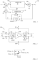
- FIG. 1 is a simplified block diagram of a ⁇ modulator 100 configured as a ⁇ analog-to-digital converter (ADC) with force-and-correction implemented according to an embodiment of the present disclosure.
- the force-and-correction is applied by injecting correction signals into the modulator loop to recover the stability for a large signal range.
- the ⁇ modulator 100 operates to convert an input analog signal U to an output digital signal V.
- U is provided to one input of an analog input combiner 102 having an output providing an adjusted input signal AIN.
- AIN is provided to an input of loop filter circuitry 104 having an output providing a filtered signal F.
- F is provided to an input of an ADC 106 having an output providing the output digital signal V.
- the ADC 106 operates at a sampling frequency FS.
- the loop filter circuitry 104 may be configured as continuous-time or discrete type filters.
- V is fed back to an input of force circuitry 108 that performs a force algorithm for converting V to an output force signal FC in response to a force control signal FFORCE.
- FFORCE may be a frequency signal that is the same as a chopping frequency FCHOP for configurations using chopping, but may also be a different frequency or have a form controlled by a digital algorithm as further described herein.
- the force algorithm periodically forces its output to a predetermined force state which may be zero or non-zero and which may be fixed or variable, referred to herein as a predetermined force state.
- V and FC are provided to respective inputs of a digital combiner 110 having an output providing an error signal E.
- the combiner 110 operates as an adder which subtracts FC from V to generate the error signal E.
- the error signal E is provided to an input of force correction circuitry 112, which generates at least one error correction (EC) signal.
- the EC signal(s) are provided to respective inputs of the loop filter circuitry 104.
- an EC signal may also be provided to an input of the input combiner 102.
- FC is provided to an input of a digital to analog converter (DAC) 114 operating at frequency FS, in which the DAC 114 has an output providing a first analog feedback signal AFB1.
- AFB1 is provided to another input of the input combiner 102.
- the input combiner 102 is configured as an adder which subtracts AFB1 from U to generate the adjusted input signal AIN.
- the input combiner 102 may also be configured to subtract the EC signal from U to generate AIN.
- the loop filter circuitry 104 may include one or more integrators or the like in which at least one integrator which may further include chopping as further described herein.
- the loop filter circuitry 104 may be implemented as a cascade of integrators coupled in series.
- only the initial integrator of the cascade of integrators incorporates the chopping function, although the chopping function may be applied to one or more integrators or loop filters within the loop filter circuitry 104.
- the ⁇ modulator 100 may be clocked at increasingly higher rates such as approaching the gigahertz (GHz) range, taking benefit from the speed capabilities of advanced technology fabrication methods.
- GHz gigahertz
- the 1/f flicker noise contribution of small devices increasingly dominates thermal noise causing errors.
- choppers are included to employ chopping to mitigate the 1/f noise.
- the frequency of FCHOP should also be relatively high, causing the choppers to be prone to nonidealities such as duty cycle error and time skew and the like.
- spectral content such as out-of-band interferers and high-frequency quantization noise that is present at FCHOP or multiples thereof can be partly downfolded in the signal band thereby degrading modulator noise, spectral purity, and interference robustness.
- the force circuitry 108 is included to periodically force the ⁇ modulator 100 to a predetermined force state to facilitate chopper switching or other causes.
- the predetermined force state may be a zero state or non-zero state, which may be any DC-state (including the zero state) or a variable state, which is generally referred to herein as a predetermined force state.
- Such force application injects periodic errors in the ⁇ loop.
- the force correction circuitry 112 is included to compensate and reduce these periodic errors.
- Various embodiments of the force correction circuitry 112 are described herein for receiving the force error signal E and applying one or more force correction signals EC in the loop for correcting the force error caused by the force circuitry 108.
- E may be converted to an analog signal and may also be multiplied by a gain factor to develop EC which is applied at various locations in the loop to implement force-and-correction as further described herein.
- FIG. 2 is a schematic diagram of an integrator 200 that may be used within the loop filter circuitry 104 according to one embodiment of the present disclosure.
- the illustrated configuration of the integrator 200 is exemplary only in which it is understood that many different integrator configurations may be used.
- the input and output signals of the integrator 200 have a differential or pseudo-differential signal form in which each of two analog choppers 218 and 220 are configured to swap the polarities of the respective signals at the chopper frequency FCHOP.
- the output of the integrator 200 is an integrated signal INT, which may be provided to additional loop filters within the loop filter circuitry 104 for developing the filtered signal F.
- the integrator 200 may be implemented without chopping in which the analog choppers 218 and 220 are not provided as further described herein.
- the input signal AIN includes a positive polarity provided to a first end of a resistor 202 with a resistance R1 and includes a negative polarity provided to a first end of another resistor 204 with a resistance R2.
- the other end of the resistor 202 is coupled to a node 203 which is further coupled to a first input I1 of the analog chopper 218 and to one end of a capacitor 206 with a capacitance C1.
- the other end of the resistor 204 is coupled to a node 205 which is further coupled to a second input I2 of the analog chopper 218 and to one end of a capacitor 208 with a capacitance C2.
- the nodes 203 and 205 form the positive and negative polarities of a voltage V1.
- the analog chopper 218 has first and second outputs O1 and O2 coupled to noninverting and inverting inputs, respectively, of an amplifier 210.
- the amplifier 210 has inverting and noninverting outputs coupled to first and second inputs I1 and I2, respectively, of the chopper 220.
- the chopper 220 has a first output O1 coupled to an output node 211 forming a negative polarity of output voltage INT, in which node 211 is further coupled to the other end of the capacitor 206.
- the analog chopper 220 has a second output O2 coupled to another output node 213 forming a positive polarity of INT, in which node 213 is further coupled to the other end of the capacitor 208.
- the polarities of INT are provided to corresponding polarity inputs (not shown) of a next component within the loop filter circuitry 104.
- node 203 is coupled to the noninverting input and node 205 is coupled to the inverting input of the amplifier 210, while the inverting and noninverting outputs of the amplifier 210 are provided to output nodes 211 and 213, respectively.
- the general configuration of the integrator 200 with or without chopping may be used to implement additional cascaded integrators in the loop filter circuitry 104 with the same or with different transfer functions.
- FIG. 3 is a simplified block diagram of the force circuitry 108 implemented according to one embodiment of the present disclosure.
- the force circuitry 108 includes an internal switch that switches between a predetermined force state (PFS) and an input value IN at the rate of FFORCE for providing an output value OUT.
- PFS predetermined force state
- DC is 0 (force-to-zero) although alternative non-zero fixed or variable values are contemplated.
- IN is the V signal which is the output of the ⁇ modulator 100
- OUT is FC, which is the force signal FC provided to the input of the DAC 114.
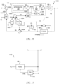
- FIG. 4 is a simplified block diagram of a ⁇ modulator 400 configured as a ⁇ ADC with force-and-correction implemented according to one embodiment of the present disclosure.
- the ⁇ modulator 400 is substantially similar to the ⁇ modulator 100 in which similar components assume identical reference numbers.
- the input combiner 102, the loop filter circuitry 104, the ADC 106, the force circuitry 108, the combiner 110 and the DAC 114 are included and coupled in substantially similar manner for converting U to V.
- the loop filter circuitry 104 may or may not be implemented with chopping.
- the force correction circuitry 112 is implemented as force correction circuitry 412 including delay circuitry 402 operating at frequency FS and a digital combiner 404.
- the delay circuitry 402 may be replaced by an arbitrary filter, such as a FIR filter or the like which may or may not be clocked. It is noted that the delay imposed by the delay circuitry 402 may be any type of delay, such as a fractional delay, a delay of one clock cycle, a delay of multiple clock cycles, etc. The delay may be a phase shift or the like and may be implemented as a filter for shaping the response.
- the error signal E is provided to an input of the delay circuitry 402 having an output providing a delayed error signal DE.
- the FC and DE signals are provided to respective inputs of the combiner 404 having an output providing a digital feedback signal FB.
- the combiner 404 is an adder which adds DE and FC to generate FB, which is provided instead of FC to the input of the DAC 114 for generating the first analog feedback signal AFB1.
- the DAC 114 injects a correction signal in the form of DE in the next FS clock cycle after the force phase.
- This correction signal is generated by delaying the force error signal E to provide the DE signal, which is then added to the input via the input combiner 102 via the DAC 114.
- the DAC 114 may be configured as a FIRDAC or the like. Since this correction signal DE is delayed, however, part of the maximum stable input of the ⁇ modulator 400 may be lost because the force error is not fully compensated. Nonetheless, substantial improvement over conventional configurations may be achieved.
- FIG. 5 is a simplified block diagram of a ⁇ modulator 500 configured as a ⁇ ADC with force-and-correction implemented according to another embodiment of the present disclosure.
- the ⁇ modulator 500 is substantially similar to the ⁇ modulator 400 in which similar components assume identical reference numbers.
- the input combiner 102, the loop filter circuitry 104, the ADC 106, the force circuitry 108, the adder 110, the delay circuitry 402 and the DAC 114 are included and coupled in substantially similar manner for converting U to V.
- the loop filter circuitry 104 may or may not be implemented with chopping.
- the force correction circuitry 112 is implemented as force correction circuitry 512 including the delay circuitry 402 and another DAC 504 that replaces the combiner 404.
- the DAC 504 has an input receiving the delayed error signal DE and has an output providing a second analog feedback signal AFB2 to another input of the input combiner 102.
- FC is provided directly to the input of the DAC 114.
- the input combiner 102 is configured as an adder which subtracts both AFB1 and AFB2 from U to generate AIN.
- the DAC 504 injects a correction signal in the form of DE after the delay.
- This correction signal is generated by delaying the force error signal E to provide the DE signal, which is then added to the input via the input combiner 102 via the DAC 504 rather than the DAC 114.
- Each one or both of the DACs 114 and 504 may be configured as a FIRDAC or the like.
- the ⁇ modulator 500 is similar to the ⁇ modulator 400 in that since the correction signal DE is delayed, part of the maximum stable input of the ⁇ modulator 500 may be lost because the force error is not fully compensated. Nonetheless, substantial improvement over conventional configurations is achieved.
- FIG. 6 is a simplified block diagram of a ⁇ modulator 600 configured as a ⁇ ADC with force-and-correction implemented according to another embodiment of the present disclosure.
- the ⁇ modulator 600 is similar to the ⁇ modulator 400 in which similar components assume identical reference numbers.
- the input combiner 102, the loop filter circuitry 104, the ADC 106, the force circuitry 108, the adder 110, the delay circuitry 402, the combiner 404 and the DAC 114 are included and coupled in substantially similar manner for converting U to V.
- the loop filter circuitry 104 may or may not be implemented with chopping.
- the force correction circuitry 112 is implemented as force correction circuitry 612 which includes the delay circuitry 402, the combiner 404, and another DAC 602.
- the delay circuitry 402 and the combiner 404 are coupled to operate in a substantially similar manner previously described for feeding DE through the DAC 114 to the input combiner 102.
- the error signal E is additionally provided to an input of the DAC 602 having an output providing a first analog version of E, shown as EA1, which is provided to a selected input of the loop filter circuitry 104 to implement further force error correction.
- the INT signal is provided to an input of a loop filter (LF) 604 having an output providing a preliminary filtered signal PF to an input of an analog output combiner 606.
- An amplifier 608 with gain a1 has an input receiving INT and an output providing an amplified signal AN to another input of the combiner 606.
- the output combiner 606 combines the PF, AN and EA1 signals to generate and provide the filtered signal F to the ADC 106.
- the output combiner 606 operates as an adder which adds PF and AN and subtracts EA1 to generate F. The conversion of E into EA1 by the DAC 602 provides additional compensation for the force error.
- the error compensation using both of the DACs 114 and 602 achieves a more stable input at higher frequencies with reduced performance degradation.
- the DACs 114 and 602 may each have separate gain factors, such as 1x or other gain that is empirically determined for best results.
- the DAC 602 may be configured as a multi-tap FIRDAC or the like.
- the loop filter 604 may be configured in any suitable manner, such as resonators, biquad filters, integrators, etc.
- the loop filter 604 may also be configured as one or more continuous-time filters or discrete filters or the like.
- the loop filter 604 includes one or more additional integrators in which the loop filter circuitry 104 may be configured as a series of cascaded integrators or the like with or without chopping.
- the gain factor a1 of the amplifier 608 is a feedforward coefficient having a value that is selected to stabilize the loop and ensure first-order behavior of the ⁇ modulator 600 at higher frequencies.
- the ⁇ modulator 600 is configured with feedback error correction similar to the ⁇ modulator 400 in which an analog version of DE is fed to the input combiner 102 via the combiner 404 and the DAC 114.
- the feedback error correction of the ⁇ modulator 600 may instead be configured similar to the ⁇ modulator 500 in which an analog version of DE is fed to the input combiner 102 via the additional DAC 504.
- FIG. 7 is a simplified block diagram of another ⁇ modulator 700 configured as an ⁇ ADC with force-and-correction implemented according to another embodiment of the present disclosure.
- the ⁇ modulator 700 is substantially similar to the ⁇ modulator 600 in which similar components assume identical reference numbers.
- the input combiner 102, the loop filter circuitry 104, the ADC 106, the force circuitry 108, the adder 110, the delay circuitry 402, the combiner 404 and the DAC 114 are included and coupled in substantially similar manner for converting U to V.
- the loop filter circuitry 104 may or may not be implemented with chopping.
- the loop filter circuitry 104 further includes an analog intermediate combiner 702 inserted between the integrator 200 and the loop filter 604.
- the intermediate combiner 702 has a first input receiving INT, a second input receiving a feed forward error signal EA2, and an output providing an adjusted integration signal INTA to the input of the loop filter 604.
- the force correction circuitry 112 is implemented as force correction circuitry 712 which is similar to the force correction circuitry 612 with the addition of another DAC 704 having in input receiving the error signal E and having an output providing EA2 provided to the intermediate combiner 702.
- the intermediate combiner 702 is configured as an adder which subtracts EA2 from INT to generate INTA.
- the ⁇ modulator 700 achieves further correction as compared to the ⁇ modulator 600 that may be caused by loss of charge in an integrator or within any other filter contained within the loop filter 604. Such error is a residual error that may be reduced by the feedback loop but that nonetheless causes a reduction of performance.
- the DAC 704 provides EA2 to account for the charge loss or other residual error due to incomplete error correction.
- EA2 may be an average error signal with suitable gain scaled to minimize the residual error. It is noted that gain selection is scaled based on loop filter coefficients.
- the DAC 602 may also be configured as a multi-tap FIRDAC or the like.
- FIG. 8 is a simplified block diagram of another ⁇ modulator 800 configured as an ⁇ ADC with force-and-correction implemented according to another embodiment of the present disclosure.
- the ⁇ modulator 800 is substantially similar to the ⁇ modulator 700 in which similar components assume identical reference numbers.
- the loop filter circuitry 104 may or may not be implemented with chopping.
- the force correction circuitry 112 is implemented as force correction circuitry 812 which includes the DACs 602 and 704 along with the DAC 504 in which FC is provided directly to the input of the DAC 114.
- the DAC 504 has an input receiving the delayed error signal DE and has an output providing the second analog feedback signal AFB2 to another input of the input combiner 102 in a similar manner as the ⁇ modulator 500.
- the input combiner 102 is configured as an adder which subtracts both AFB1 and AFB2 from U to generate AIN.
- the DAC 504 of the ⁇ modulator 800 may be used to provide additional compensation for these residual errors.
- the DAC 504 may provide simple fine-tuning sufficient to gain back the full maximum stable input range of the modulator, without the need for full compensation of the force error. Compensation can be adapted by adjusting the gain of the DAC 504. In one embodiment, for example, for certain loop filter coefficients the gain of the DAC 504 may be set to about 1.25, although alternative gain factors are contemplated for different loop filter coefficients.
- further compensation may be achieved by adding a linear component via the DAC 704 by implementing it as a multi-tap FIRDAC.
- Either one or both of the DACs 504 and 602 may also be implemented as multi-tap FIRDACs as well. It is noted that more compensation signals may be injected at other nodes in the loop filter circuitry 104 employing additional DACs or FIRDACs (not shown).
- FIG. 9 is a simplified block diagram of another ⁇ modulator 900 configured as an ⁇ ADC with force-and-correction implemented according to another embodiment of the present disclosure.
- the ⁇ modulator 900 is substantially similar to the ⁇ modulator 800 in which similar components assume identical reference numbers.
- the loop filter circuitry 104 may or may not be implemented with chopping.
- the force correction circuitry 112 is also implemented as force correction circuitry 812. It is noted that the error correction signal EA2 injected at the intermediate combiner 702 may cause a first-order shaped noise in the output signal V.
- the ⁇ modulator 900 further includes a digital noise cancelation filter (NCF) 902 having an input receiving the error signal E and an output providing a filter digital error signal FE.
- NCF digital noise cancelation filter
- the ⁇ modulator 900 further includes a digital output combiner 904 having a first input receiving signal V, another input receiving signal FE, and an output providing an adjusted output signal VA.
- the output combiner 904 may be configured as a digital adder that adds FE to V to generate VA.
- the NCF 902 may be configured to remove the noise injected by the correction signal EA2.
- the NCF 902 may be configured as a 2-tap FIR filter with coefficients [0.5 0.5] to remove the injected noise, although alternative coefficients values may be used in different configurations.
- the gain of the DAC 704 and the coefficient gains of the NCF 402 may be configured to match each other for good noise cancellation. The accuracy of the gains of each of the other error DACs 114, 602 and 504 may have relatively wide variances.
- FIG. 10 is a simplified block diagram of another ⁇ modulator 1000 configured as an ⁇ ADC with force-and-correction implemented according to yet another embodiment of the present disclosure.
- the ⁇ modulator 1000 includes similar components as the ⁇ modulator 600 in which similar components assume identical reference numbers.
- the ⁇ modulator 1000 includes the input combiner 102, the loop filter circuitry 104, the ADC 106, the force circuitry 108, the force combiner 110, and the DAC 114 coupled in substantially the same manner, in which the loop filter circuitry 104 includes the integrator 200 with or without choppers, the intermediate combiner 702, the loop filter 604, the amplifier 608 and the output combiner 606 coupled in substantially similar manner for converting the analog input signal U to the digital output signal V.
- the force correction circuitry 112 for the ⁇ modulator 1000 is implemented as force correction circuitry 1012 which includes the delay circuitry 402 and the digital combiner 404 providing FB to the DAC 114, along with additional DACs 1002 and 1004, an analog combiner 1006, and another integrator 1008 which is configured in substantially identical manner as the integrator 200 without choppers and having the same transfer function.
- the DAC 1002 has an input receiving DE and an output providing a signal DEA
- the DAC 1004 has an input receiving E and an output providing a signal EB.
- the combiner 1006 combines the DEA and EB signals to provide an output feedback signal FB1, which is provided to an input of the integrator 1008. In one embodiment, EB is subtracted from DEA by the combiner 1006 to develop FB1.
- the integrator 1008 provides an integrated feedback signal FBINT to the other input of the intermediate combiner 702.
- the DACs 1002 and 1004 may have any suitable gains determined empirically to achieve best results in a given configuration.
- the DACs 1002 and 1004 may be configured as multi-tap FIRDACs or the like.
- the integrator 1008 is a replica of the first integrator 200 (except without choppers) and is added to create a triangular compensation signal FBINT, which is added to INT to generate a modified adjusted integrated signal INTA' at the output of the intermediate combiner 702.
- a drawback of the ⁇ modulator 1000 is that the extra integrator 1008 operates in an open-loop condition.
- the output FBINT may drift away and clip to the supply voltage if this offset is not counteracted with an additional control loop.
- FIG. 11 is a simplified block diagram of an alternative force algorithm configuration 1102 implemented the according to another embodiment of the present disclosure.
- the force circuitry 108 is included having an input receiving V and an output providing FC in a similar manner as previously described.
- a digital algorithm (DA) block 1102 is also included having a first input receiving V, a second input receiving an external signal W, and an output providing a force signal FRC provided to the "clock" input of the force circuitry 108.
- the DA block 1102 generates FRC based on one or both of V and W for asserting the force algorithm.
- the force algorithm configuration 1102 may be used instead of only the force circuitry 108 in any of the ⁇ modulator configurations described herein.
- circuitry states such as circuitry low and circuitry high may be reversed depending upon whether the pin or signal is implemented in positive or negative circuitry or the like.
- the circuitry state may be programmable in which the circuitry state may be reversed for a given circuitry function.
Landscapes
- Engineering & Computer Science (AREA)
- Theoretical Computer Science (AREA)
- Compression, Expansion, Code Conversion, And Decoders (AREA)
Applications Claiming Priority (1)
| Application Number | Priority Date | Filing Date | Title |
|---|---|---|---|
| US17/880,868 US12015426B2 (en) | 2022-08-04 | 2022-08-04 | System and method of reducing delta-sigma modulator error using force-and-correction |
Publications (1)
| Publication Number | Publication Date |
|---|---|
| EP4329201A1 true EP4329201A1 (de) | 2024-02-28 |
Family
ID=87340766
Family Applications (1)
| Application Number | Title | Priority Date | Filing Date |
|---|---|---|---|
| EP23185554.5A Pending EP4329201A1 (de) | 2022-08-04 | 2023-07-14 | System und verfahren zur verringerung von delta-sigma-modulatorfehlern unter verwendung von kraft- und korrektur |
Country Status (3)
| Country | Link |
|---|---|
| US (1) | US12015426B2 (de) |
| EP (1) | EP4329201A1 (de) |
| CN (1) | CN117526955A (de) |
Families Citing this family (2)
| Publication number | Priority date | Publication date | Assignee | Title |
|---|---|---|---|---|
| US20260066918A1 (en) * | 2024-09-04 | 2026-03-05 | Nxp B.V. | Continuous-Time Delta-Sigma Modulator with Capacitive Feed-ins |
| US20260066919A1 (en) * | 2024-09-04 | 2026-03-05 | Nxp B.V. | High-Speed Continuous-Time Delta-Sigma Modulator Including an Amplifier with Limited Gain |
Citations (3)
| Publication number | Priority date | Publication date | Assignee | Title |
|---|---|---|---|---|
| EP3280055A1 (de) * | 2016-08-05 | 2018-02-07 | MediaTek Inc. | Delta-sigma-modulator mit delta-sigma-trunkator und zugehöriges verfahren zur verringerung der leckfehler eines delta-sigma-modulators |
| EP3709518A1 (de) * | 2019-03-14 | 2020-09-16 | MediaTek Inc. | Delta-sigma-modulator mit trunkierungsfehlerkompensation und zugehöriges verfahren |
| US20200343904A1 (en) * | 2017-12-29 | 2020-10-29 | Robert Bosch Gmbh | Power Reduction and Performance Enhancement Techniques for Delta Sigma Modulator |
Family Cites Families (18)
| Publication number | Priority date | Publication date | Assignee | Title |
|---|---|---|---|---|
| US6304608B1 (en) * | 1998-11-04 | 2001-10-16 | Tai-Haur Kuo | Multibit sigma-delta converters employing dynamic element matching with reduced baseband tones |
| US6724332B1 (en) * | 2002-08-13 | 2004-04-20 | Cirrus Logic, Inc. | Noise shaping circuits and methods with feedback steering overload compensation and systems using the same |
| US6940436B2 (en) * | 2003-10-31 | 2005-09-06 | Texas Instruments Incorporated | Analog-to-digital conversion system with second order noise shaping and a single amplifier |
| JP2006140600A (ja) * | 2004-11-10 | 2006-06-01 | Fujitsu Ltd | シグマデルタa/d変換器 |
| JP4488951B2 (ja) * | 2005-04-26 | 2010-06-23 | 富士通株式会社 | 複素型シグマデルタアナログデジタル変換装置及び受信機 |
| US7423567B2 (en) * | 2006-09-12 | 2008-09-09 | Cirrus Logic, Inc. | Analog-to-digital converter (ADC) having a reduced number of quantizer output levels |
| US7609189B1 (en) * | 2007-04-19 | 2009-10-27 | Marvell International Ltd. | Interface for hybrid sigma-delta data converter |
| US7545303B1 (en) * | 2008-03-14 | 2009-06-09 | National Semiconductor Corporation | Sigma-delta difference-of-squares RMS-to-DC converter with forward and feedback paths signal squaring |
| JP2009290455A (ja) * | 2008-05-28 | 2009-12-10 | Toshiba Corp | Demシステム、デルタシグマa/d変換器、及び受信機 |
| US7961129B2 (en) * | 2009-08-12 | 2011-06-14 | Infineon Technologies Ag | Coupled delta-sigma modulators |
| US20140077984A1 (en) * | 2012-09-14 | 2014-03-20 | Mediatek Inc. | Delta-sigma modulator using hybrid excess loop delay adjustment scheme and related delta-sigma modulation method |
| US9184754B2 (en) * | 2013-12-12 | 2015-11-10 | Mediatek Inc. | Analog-to-digital converting device and analog-to-digital converting method |
| US9240801B2 (en) * | 2014-03-14 | 2016-01-19 | Texas Instruments Incorporated | Analog-to-digital converter |
| US10763888B1 (en) * | 2019-05-09 | 2020-09-01 | Nxp B.V. | Metastability shaping technique for continuous-time sigma-delta analog-to-digital converters |
| US10998917B1 (en) * | 2020-07-14 | 2021-05-04 | Nxp B.V. | Sigma-delta analog-to-digital converter |
| US11394395B1 (en) * | 2021-01-26 | 2022-07-19 | Nxp B.V. | Techniques for linearizing digital-to-analog converters in sigma-delta analog-to-digital converters |
| US11502699B1 (en) * | 2021-06-24 | 2022-11-15 | Nxp B.V. | System and method of calibration of sigma-delta converter using injected signal correlation |
| US11522557B1 (en) * | 2021-07-29 | 2022-12-06 | Nxp B.V. | System and method of calibration of sigma-delta converter using tone injection |
-
2022
- 2022-08-04 US US17/880,868 patent/US12015426B2/en active Active
-
2023
- 2023-07-14 EP EP23185554.5A patent/EP4329201A1/de active Pending
- 2023-08-03 CN CN202310975834.3A patent/CN117526955A/zh active Pending
Patent Citations (3)
| Publication number | Priority date | Publication date | Assignee | Title |
|---|---|---|---|---|
| EP3280055A1 (de) * | 2016-08-05 | 2018-02-07 | MediaTek Inc. | Delta-sigma-modulator mit delta-sigma-trunkator und zugehöriges verfahren zur verringerung der leckfehler eines delta-sigma-modulators |
| US20200343904A1 (en) * | 2017-12-29 | 2020-10-29 | Robert Bosch Gmbh | Power Reduction and Performance Enhancement Techniques for Delta Sigma Modulator |
| EP3709518A1 (de) * | 2019-03-14 | 2020-09-16 | MediaTek Inc. | Delta-sigma-modulator mit trunkierungsfehlerkompensation und zugehöriges verfahren |
Also Published As
| Publication number | Publication date |
|---|---|
| CN117526955A (zh) | 2024-02-06 |
| US12015426B2 (en) | 2024-06-18 |
| US20240048150A1 (en) | 2024-02-08 |
Similar Documents
| Publication | Publication Date | Title |
|---|---|---|
| US8570200B2 (en) | Continuous-time oversampled converter having enhanced immunity to noise | |
| US8570201B2 (en) | Direct feedback for continuous-time oversampled converters | |
| US9543978B2 (en) | Frequency selective circuit configured to convert an analog input signal to a digital output signal | |
| JP5510464B2 (ja) | 独立した遅延を有する複数のフィードバック経路を有する連続時間型シグマデルタ変調器 | |
| EP2410659B1 (de) | Multi-Bit-Sigma-Delta-Modulator mit reduzierter Bitzahl im Rückkopplungspfad | |
| US7084797B2 (en) | Delta sigma modulating apparatus | |
| EP4329201A1 (de) | System und verfahren zur verringerung von delta-sigma-modulatorfehlern unter verwendung von kraft- und korrektur | |
| US8223051B2 (en) | Multi-bit sigma-delta modulator with reduced number of bits in feedback path | |
| US20050068213A1 (en) | Digital compensation of excess delay in continuous time sigma delta modulators | |
| WO2015196175A1 (en) | Interleaved modulator | |
| EP4160924A1 (de) | System und verfahren zur replikation und unterdrückung von häckselfaltungsfehlern in delta-sigma-modulatoren | |
| KR20180117047A (ko) | 아날로그ㆍ디지털 변환기 및 밀리미터파 레이더 시스템 | |
| US7352311B2 (en) | Continuous time noise shaping analog-to-digital converter | |
| KR102617310B1 (ko) | 델타-시그마 변조기 및 변조 방법 | |
| Balachandran et al. | A 1.16 mW 69dB SNR (1.2 MHz BW) continuous time£ Δ ADC with immunity to clock jitter | |
| Buhmann et al. | Time-continuous delta-sigma a/d converters: From theory to practical implementation | |
| US20240364358A1 (en) | Sigma-delta modulator and method for operating a sigma-delta modulator | |
| Gao | A survey on continuous-time modulators: theory, designs and implementations | |
| Pesenti et al. | A low-power strategy for Delta-Sigma modulators |
Legal Events
| Date | Code | Title | Description |
|---|---|---|---|
| PUAI | Public reference made under article 153(3) epc to a published international application that has entered the european phase |
Free format text: ORIGINAL CODE: 0009012 |
|
| STAA | Information on the status of an ep patent application or granted ep patent |
Free format text: STATUS: THE APPLICATION HAS BEEN PUBLISHED |
|
| AK | Designated contracting states |
Kind code of ref document: A1 Designated state(s): AL AT BE BG CH CY CZ DE DK EE ES FI FR GB GR HR HU IE IS IT LI LT LU LV MC ME MK MT NL NO PL PT RO RS SE SI SK SM TR |
|
| STAA | Information on the status of an ep patent application or granted ep patent |
Free format text: STATUS: REQUEST FOR EXAMINATION WAS MADE |
|
| 17P | Request for examination filed |
Effective date: 20240828 |
|
| RBV | Designated contracting states (corrected) |
Designated state(s): AL AT BE BG CH CY CZ DE DK EE ES FI FR GB GR HR HU IE IS IT LI LT LU LV MC ME MK MT NL NO PL PT RO RS SE SI SK SM TR |