EP1425850B1 - Schaltungen und verfahren zum kompensieren von schaltverstärkern - Google Patents
Schaltungen und verfahren zum kompensieren von schaltverstärkern Download PDFInfo
- Publication number
- EP1425850B1 EP1425850B1 EP02756873A EP02756873A EP1425850B1 EP 1425850 B1 EP1425850 B1 EP 1425850B1 EP 02756873 A EP02756873 A EP 02756873A EP 02756873 A EP02756873 A EP 02756873A EP 1425850 B1 EP1425850 B1 EP 1425850B1
- Authority
- EP
- European Patent Office
- Prior art keywords
- filter
- signal
- amplifier
- generating
- adaptive filter
- Prior art date
- Legal status (The legal status is an assumption and is not a legal conclusion. Google has not performed a legal analysis and makes no representation as to the accuracy of the status listed.)
- Expired - Lifetime
Links
- 238000000034 method Methods 0.000 title claims abstract description 23
- 230000003044 adaptive effect Effects 0.000 claims abstract description 32
- 230000004044 response Effects 0.000 claims abstract description 32
- 238000012546 transfer Methods 0.000 claims abstract description 11
- 238000006243 chemical reaction Methods 0.000 claims description 9
- 230000003111 delayed effect Effects 0.000 claims description 5
- 230000007274 generation of a signal involved in cell-cell signaling Effects 0.000 claims description 2
- 238000001914 filtration Methods 0.000 claims 7
- 230000008878 coupling Effects 0.000 claims 1
- 238000010168 coupling process Methods 0.000 claims 1
- 238000005859 coupling reaction Methods 0.000 claims 1
- 230000008569 process Effects 0.000 description 7
- 230000006978 adaptation Effects 0.000 description 6
- 230000008901 benefit Effects 0.000 description 4
- 230000005236 sound signal Effects 0.000 description 3
- 238000013461 design Methods 0.000 description 2
- 238000010586 diagram Methods 0.000 description 2
- 230000001939 inductive effect Effects 0.000 description 2
- 238000012986 modification Methods 0.000 description 2
- 230000004048 modification Effects 0.000 description 2
- 238000012545 processing Methods 0.000 description 2
- 230000004308 accommodation Effects 0.000 description 1
- 230000003321 amplification Effects 0.000 description 1
- 239000003990 capacitor Substances 0.000 description 1
- 238000012937 correction Methods 0.000 description 1
- 239000013078 crystal Substances 0.000 description 1
- 230000017525 heat dissipation Effects 0.000 description 1
- 238000004519 manufacturing process Methods 0.000 description 1
- 230000007246 mechanism Effects 0.000 description 1
- 238000003199 nucleic acid amplification method Methods 0.000 description 1
- 230000010363 phase shift Effects 0.000 description 1
- 230000035945 sensitivity Effects 0.000 description 1
- 238000004088 simulation Methods 0.000 description 1
Images


Classifications
-
- H—ELECTRICITY
- H03—ELECTRONIC CIRCUITRY
- H03F—AMPLIFIERS
- H03F3/00—Amplifiers with only discharge tubes or only semiconductor devices as amplifying elements
- H03F3/20—Power amplifiers, e.g. Class B amplifiers, Class C amplifiers
- H03F3/21—Power amplifiers, e.g. Class B amplifiers, Class C amplifiers with semiconductor devices only
- H03F3/217—Class D power amplifiers; Switching amplifiers
-
- H—ELECTRICITY
- H03—ELECTRONIC CIRCUITRY
- H03F—AMPLIFIERS
- H03F1/00—Details of amplifiers with only discharge tubes, only semiconductor devices or only unspecified devices as amplifying elements
- H03F1/32—Modifications of amplifiers to reduce non-linear distortion
- H03F1/3241—Modifications of amplifiers to reduce non-linear distortion using predistortion circuits
-
- H—ELECTRICITY
- H03—ELECTRONIC CIRCUITRY
- H03F—AMPLIFIERS
- H03F3/00—Amplifiers with only discharge tubes or only semiconductor devices as amplifying elements
- H03F3/20—Power amplifiers, e.g. Class B amplifiers, Class C amplifiers
- H03F3/21—Power amplifiers, e.g. Class B amplifiers, Class C amplifiers with semiconductor devices only
- H03F3/217—Class D power amplifiers; Switching amplifiers
- H03F3/2178—Class D power amplifiers; Switching amplifiers using more than one switch or switching amplifier in parallel or in series
-
- H—ELECTRICITY
- H03—ELECTRONIC CIRCUITRY
- H03F—AMPLIFIERS
- H03F2200/00—Indexing scheme relating to amplifiers
- H03F2200/294—Indexing scheme relating to amplifiers the amplifier being a low noise amplifier [LNA]
-
- H—ELECTRICITY
- H03—ELECTRONIC CIRCUITRY
- H03F—AMPLIFIERS
- H03F2200/00—Indexing scheme relating to amplifiers
- H03F2200/331—Sigma delta modulation being used in an amplifying circuit
-
- H—ELECTRICITY
- H03—ELECTRONIC CIRCUITRY
- H03F—AMPLIFIERS
- H03F2200/00—Indexing scheme relating to amplifiers
- H03F2200/372—Noise reduction and elimination in amplifier
Definitions
- the present invention relates in general to switched mode electronic amplifiers, and in particular to circuits and methods for compensating for switched mode amplifiers.
- Class D audio power amplifiers have been used for many years in systems, such as wireline telephony, where high bandwidth is not critical.
- new fabrication techniques, and in particular, new techniques for fabricating power transistors have made integrated Class D APAs possible. This has extended their potential applications to lower-power, higher-bandwidth systems, including battery-powered portable music players and wireless communications devices.
- Class D amplifiers are their efficiency. Generally, an audio signal is converted into a relatively high frequency stream of pulses varying in width with the amplitude of the audio signal. This pulse width modulated (PWM) signal is used to switch a set of power output transistors between cutoff and saturation which results in efficiencies above ninety percent (90%). In contrast, the typical Class AB push-pull amplifier, using output transistors whose conduction varies linearly during each half-cycle, has an efficiency of around sixty percent (60%). The increased efficiency of Class D amplifiers in turn reduces power consumption and consequently lowers heat dissipation and improves battery life in portable systems.
- PWM pulse width modulated
- an amplifier system which includes a switching amplifier unit and analog conversion circuitry configured to recover an analog signal from an output signal of the switching amplifier.
- An adaptive filter coupled to an output of the conversion circuitry is configured to derive an inverse transfer function of a forward path through the amplifier system, which includes the analog conversion circuitry, the derived inverse transfer function is used to generate a coefficient map from which a compensation filter responsively compensates for variations in the output load of the amplifier unit.
- inventive concepts address a significant problem in the application of switched mode amplifiers generally, and particularly in applications in which faithful reproduction of the input signals is desired, namely the sensitivity of the frequency response of the system to the non-ideal conditions represented by realistic loads.
- these concepts allow for the implementation of compensation mechanisms which equalize the frequency response of the amplifier system in the presence of reactive loads, as well as loads with nominal impedances that span the range of values presented by different output devices that may be connected to the amplifier system.
- FIGURES 1 -4 of the drawings in which like numbers represent like parts.
- the low pass filter is of the passive type, including inductive and/or capacitive reactive elements to smooth the signal.
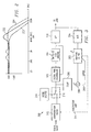
- FIGURE 1A illustrates, in block diagram form, a typical Class D amplifier system 100.
- Amplifier system 100 includes Class D amplifier 102 containing MOSFET switches 104, along with their associated gates and drivers, and PWM controller 106.
- PWM controller 106 receives a digitized audio input signal (Audio In), which constitutes the signal to be amplified.
- MOSFET switches 104 may constitute a full bridge amplifier. Alternatively other circuit designs may be used, including a half-bridge switch.
- PWM controller also receives two feedback signals. Feedback path 109 from the output of MOSFET switches 104 may be used to correct the errors introduced by non-ideal switch behavior.
- PWM signal generation techniques are discussed in coassigned U.S. Patent No.
- LPF 110 low pass filter 110
- LPF 110 is thus preferably a simple digital to analog converter.
- One possible application of audio amplifier 100 is in a digital radio 110, such as that shown in FIGURE 1B.
- Digital radio 110 includes an analog section or front-end 111 which receives radio frequency (RF) signals from an associated antenna 112.
- Analog front-end 111 is preferably a conventional RF down-converter including a low noise amplifier (LNA) 113 for setting the system noise figure, a bandpass filter 114 and mixer 115 driven by an analog local oscillator 116. The mixed-down analog signal is then converted into digital form by analog to digital converter 117.
- LNA low noise amplifier
- the digitized data output from A / D converter 117 is passed to digital processing section 118.
- a pair of mixers 119a,b generate in-phase (I) and quadrature (Q) signals from a corresponding pair of clock phases from crystal oscillator 120.
- the I and Q signals are next passed through bandpass filters 121a and 121b on to digital baseband processor 122.
- the processed digital signal is then reconverted to analog (audio) form by D/A converter 123.
- a switched mode (Class D) audio power amplifier (APA) 124 is used to drive an external set of speakers or a headset.
- APA switched mode audio power amplifier
- SMPS switched mode power supply
- the corner frequency of LPF 110 should be just above the passband of the amplifier system. However, this increases the error in the frequency response in the passband. Moreover, the frequency response is significantly affected by the load impedance, Z.
- FIGURE 2 illustrates typical frequency response curves.
- Curves 200 and 202 are typical frequency responses with eight and sixteen ohm resistive loads, respectively. With a significant inductive component, which may be typical of audio amplification into speakers, a response of the form in curve 204 may result. Curve 204 exhibits a significant passband ripple. (The frequencies and gain levels shown in FIGURE 2 are approximate and are provided as general reference to the depicted curves.)
- a feedback path 112 from the output of LPF may be provided to compensate for frequency response modifications introduced by LPF 110.
- the load, Z has a significant reactive component. Consequently, the phase shift of the filter is not well known, which exacerbates the question of the stability of the feedback loop.
- feedback path 112 must include, an analog to digital (A/D) converter (not shown in FIGURE 1.) This adds additional phase delay, further complicating the performance/stability trade off.
- Amplifier system 300 includes switching amplifier 102 and LPF 110 coupled to the load (not shown in FIGURE 3).
- Amplifier system 300 includes adaptive filter 302, which may be a digital filter.
- the input to adaptive filter 302 is provided by the output of LPF 110 via analog-to-digital converter (A/D) 304.
- A/D 304 outputs a digital representation of the analog audio signal from LPF 110.
- Adaptive filter 302 may be a finite impulse response (FIR) filter that "learns" the inverse of the transfer function of the forward path through amplifier system formed by switching amplifier 102, LPF 110 and the load (not shown in FIGURE 3). Adaptive filter 302 derives the inverse transfer function by adjusting the FIR coefficients, as discussed below. Because the transfer function of LPF 110 is substantially all pole in nature, a FIR implementation of adaptive filter 302 is a good inverse, the FIR being an all zero filter. Filter 302 is adapted such that the combined forward path, including switching amplifier 102, LPF 110, the load, and adaptive filter 302 is equivalent to a pure delay. The signal input to switching amplifier 102 is equivalently delayed in delay 306. The frequency response of delay element 306 is flat. The output of delay element 306 is differenced with the output of adaptive filter 302 in adder 308. The output of adder 308 provides error signal 310 to adaptive filter 302.
- FIR finite impulse response
- Adaptive filter 302 adjusts the coefficients of the FIR in response to error signal 310.
- the adaptive filter adjusts the coefficients so as to drive the error signal towards zero.
- One such algorithm for adjusting the coefficients known in the signal processing art, is the least-mean-square (LMS) algorithm; however, it should be recognized that other adaptation algorithms may also be used in alternative embodiments.
- LMS least-mean-square
- the order of compensating filter 312 may be in the range of from four (4) to ten (10). This range is exemplary, and longer filters may be implemented, in alternative embodiments of the present invention, to accommodate loads that have substantial reactive components, or to accommodate embodiments having more complex output filters, that is, filters having increased numbers of poles.
- the order of compensation filter depends on the desired flatness of the filter response; the longer the filter the more compensation that is possible.
- MATLAB simulations have shown that an audio load of 4-16 ohms plus a reactive component can be suitably compensated for with a 6th order filter.
- the signal to be amplified is input to compensation filter 312.
- the coefficients from adaptive filter 302 are mapped to the coefficients of compensation filter 312, indicated by the dashed path coefficient, coefficient map 314, in FIGURE 3.
- the present invention provides a closed loop feedback compensation in which the loop is closed by the coefficient map 314.
- Compensation filter 312 thus, also has a transfer function that is the inverse of the forward path through switching amplifier system 300. Consequently, the output signal of the loaded amplifier system is flat over the bandwidth of the loop.
- Compensation filter 312 may be, in an embodiment of the present invention a FIR.
- compensation filter 312 coefficient map 314 may be a one-one copying of the coefficients of adaptive filter 302 to filter 312.
- filter 312 may also be implemented as in infinite impulse response (IIR) digital filter, and in yet another alternative embodiment implemented in the analog domain, as, for example, a switched capacitor filter.
- IIR infinite impulse response
- System 300 also includes noise source 314 and switch 316.
- the input to switching amplifier 102 may be switched between noise source 314 and the output of compensation filter 312, as discussed further below. In normal operation, the switch selects the output from compensation filter 312.
- FIGURE 4 is a flow chart of an adaptation (or calibration) methodology 400 in accordance with an embodiment of the present invention.
- Step 402 a determination is made if the system is initializing on power-up, or if user initiated adaptation has been requested.
- the user may, for example, elect to train the compensation filter when the system is installed, or, if the load is changed.
- Step 404 process 400 switches to the noise source.
- switch 316 couples the input of switching amplifier 102 to noise source 314.
- the coefficients of the adaptive filter such as filter 402, FIGURE 3 are adjusted, as long as the calibration cycle has not expired.
- Step 406 the input to the switching amplifier, such as switching amplifier 102, is switched to the signal source, Step 408.
- the signal source in accordance with system 300, is the output of compensation filter 312. Additionally, in Step 410, the coefficients of the adaptive filter are mapped into the compensation filter. Process 400 then returns to step 402.
- Adaption process 400 may also continuously adapt the switch mode amplifier system. If, in Step 402, neither a system power up event nor user demanded calibration event has occurred, then in Step 412, a determination is made as to continuous adaptation is enabled. If not, process 400 loops back to Step 402. Otherwise, process 400 proceeds to Step 413 and adjusts the coefficients of the adaptive filter, such as filter 302. In Step 410, the adaptive filter coefficients are mapped to the compensation filter. Process 400 then continuously loops between Steps 410, 402 and 412 to continuously adapt the switch mode amplifier system. The continuous adaptation may be interrupted by a user elected calibration at Step 402, as process 400 loops.
Landscapes
- Engineering & Computer Science (AREA)
- Power Engineering (AREA)
- Physics & Mathematics (AREA)
- Nonlinear Science (AREA)
- Amplifiers (AREA)
- Filters That Use Time-Delay Elements (AREA)
Claims (14)
- Verstärkersystem umfassend:einen Pulsweitenmodulator (104, 106) zur Erzeugung eines pulsweitenmodulierten Signals in Reaktion auf ein Modulatoreingangssignal;eine Analogwandlerschaltung (110) zur Erzeugung eines analogen Signals von dem pulsweitenmodulierten Signal und zur Bereitstellung einer Verstärkerausgabe zur Ansteuerung einer Last;eine Verzögerungsschaltung (306) mit einer flachen Antwort zur Verzögerung des Modulatoreingangssignals um einen ausgewählten Betrag zur Erzeugung eines verzögerten Signals;einen adaptiven Filter (302) zur Ableitung einer Koeffizientenabbildung in Reaktion auf ein Fehlersignal und ein Verstärkerausgangssignal, welche ein Inverses einer Vorwärts-Transferfunktion durch das Verstärkersystem repräsentiert, wobei der adaptive Filter weiterhin ein Ausgangssignal des adaptiven Filters generiert beinhaltend einen Verzögerungsbetrag relativ zu dem Modulatoreingangssignal als Folge einer Variation in einer Last, die durch die Verstärkerausgabe angesteuert wird;eine Fehlersignal-Erzeugungsschaltung (308) zur Erzeugung des Fehlersignals von einer Differenz zwischen dem verzögerten Signal und dem Ausgangssignal des adaptiven Filters; undeine Kompensationsschaltung (312) zum Empfangen eines Eingangssignals des Verstärkersystems und der Koeffizientenabbildung zur Erzeugung des Modulatoreingangssignals mit einer Kompensation der Variation in der Last, die an dem Verstärkerausgang angesteuert wird.
- Verstärkersystem nach Anspruch 1, weiterhin umfassend einen Analog-Digital-Wandler (304) zur Kopplung des Ausgangs der Analogwandlerschaltung (110) und des adaptiven Filters.
- Verstärkersystem nach Anspruch 1, wobei der adaptive Filter (302) einen digitalen Filter aufweist, der in Reaktion auf einen Satz von Koeffizienten betrieben wird, die ausgewählt sind, um das Fehlersignal zu minimieren, und wobei wenigstens manche der Koeffizienten die Koeffizientenabbildung umfassen.
- Verstärkersystem nach Anspruch 3, wobei der digitale Filter (302) einen Finite-Impuls-Antwort-Filter aufweist.
- Verstärkersystem nach Anspruch 3, wobei der digitale Filter (302) einen Infinite-Impuls-Antwort-Filter aufweist.
- Verstärkersystem nach Anspruch 1, wobei die Analogwandlerschaltung (110) einen Tiefpassfilter aufweist.
- Verstärkersystem nach Anspruch 1, wobei der Kompensationsfilter (312) einen Finite-Impuls-Antwort-Filter aufweist.
- Verfahren zur Kompensation von Lastvariationen in einem Schaltverstärkersystem, umfassend:Erzeugung eines pulsweitenmodulierten Signals mit einem Pulsweitenmodulator (104, 106) in Reaktion auf ein Modulatoreingangssignal;Erzeugung eines Verstärkerausgangssignals von dem pulsweitenmodulierten Signal mit einer Analogwandlerschaltung (110);Verzögern des Modulatoreingangssignals mit einer Verzögerungsschaltung (306) mit einer flachen Antwort, um ein verzögertes Signal zu generieren;Ableiten einer Koeffizientenabbildung mit einem adaptiven Filter (302) in Reaktion auf ein Fehlersignal und das Verstärkerausgangssignal, die ein Inverses einer Vorwärts-Transferfunktion durch das Verstärkersystem repräsentiert;Erzeugung eines Ausgangssignals des adaptiven Filters mit dem adaptiven Filter (302) beinhaltend einen Verzögerungsbetrag relativ zu dem Modulatoreingangssignal als Folge einer Variation in einer Last, die durch das Verstärkerausgangssignal angesteuert wird;Erzeugung des Fehlersignals von einer Differenz zwischen dem verzögerten Signal und dem Ausgangssignal des adaptiven Filters; undErzeugung des Modulatoreingangssignals von einem empfangenen Verstärkereingangssignal, wobei das Modulatoreingangssignal in Reaktion auf die Koeffizientenabbildung im Hinblick auf die Variation in der Last, die durch das Verstärkerausgangssignal angesteuert wird, kompensiert ist.
- Verfahren nach Anspruch 8, weiterhin umfassend das Durchführen einer Analog-Digital-Wandlung, um das Verstärkerausgangssignal von einer analogen in eine digitale Form zur Bereitstellung an den adaptiven Filter zu wandeln.
- Verfahren nach Anspruch 8, wobei die Erzeugung einer Koeffizientenabbildung mit einem adaptiven Filter umfasst:Filtern des Verstärkerausgangssignals mit einem digitalen Filter (302), der in Reaktion auf einen Satz von Filterkoeffizienten betrieben wird;Variieren des Satzes von Koeffizienten, um ein Niveau des Fehlersignals zu minimieren; undErzeugung der Koeffizientenabbildung aus wenigstens manchen der Filterkoeffizienten.
- Verfahren nach Anspruch 10, wobei die Filterung des Verstärkerausgangssignals mit einem digitalen Filter ein Filtern mit einem Finite-Impuls-Antwort-Filter umfasst.
- Verfahren nach Anspruch 10, wobei die Filterung der Verstärkerausgabe mit einem digitalen Filter ein Filtern mit einem Infinite-Impuls-Antwort-Filter umfasst.
- Verfahren nach Anspruch 8, wobei die Durchführung der Analogwandlung eine Filterung des pulsweitenmodulierten Signals mit einem Tiefpassfilter (110) umfasst.
- Verfahren nach Anspruch 8, wobei die Erzeugung des Modulatoreingangssignals ein Filtern des Verstärkereingangssignals mit einem Finite-Impuls-Antwort-Filter (312) mit Filterkoeffizienten, die durch die Koeffizientenabbildung gesteuert werden, umfasst.
Applications Claiming Priority (3)
| Application Number | Priority Date | Filing Date | Title |
|---|---|---|---|
| US09/927,808 US6593806B1 (en) | 2001-08-10 | 2001-08-10 | Circuits and methods for compensating switched mode amplifiers |
| US927808 | 2001-08-10 | ||
| PCT/US2002/024397 WO2003015263A1 (en) | 2001-08-10 | 2002-08-01 | Circuits and methods for compensating switched mode amplifiers |
Publications (3)
| Publication Number | Publication Date |
|---|---|
| EP1425850A1 EP1425850A1 (de) | 2004-06-09 |
| EP1425850A4 EP1425850A4 (de) | 2005-12-07 |
| EP1425850B1 true EP1425850B1 (de) | 2007-05-09 |
Family
ID=25455284
Family Applications (1)
| Application Number | Title | Priority Date | Filing Date |
|---|---|---|---|
| EP02756873A Expired - Lifetime EP1425850B1 (de) | 2001-08-10 | 2002-08-01 | Schaltungen und verfahren zum kompensieren von schaltverstärkern |
Country Status (6)
| Country | Link |
|---|---|
| US (1) | US6593806B1 (de) |
| EP (1) | EP1425850B1 (de) |
| JP (1) | JP2004538701A (de) |
| AT (1) | ATE362218T1 (de) |
| DE (1) | DE60220071T2 (de) |
| WO (1) | WO2003015263A1 (de) |
Families Citing this family (33)
| Publication number | Priority date | Publication date | Assignee | Title |
|---|---|---|---|---|
| JP3896894B2 (ja) * | 2002-05-13 | 2007-03-22 | ソニー株式会社 | 電力増幅装置 |
| US7248649B2 (en) * | 2003-06-25 | 2007-07-24 | Interdigital Technology Corporation | Digital baseband receiver including a time domain compensation module for suppressing group delay variation distortion incurred due to analog low pass filter deficiencies |
| US6885330B2 (en) * | 2003-09-05 | 2005-04-26 | Cirrus Logic, Inc. | Data converters with ternary pulse width modulation output stages and methods and systems using the same |
| JP2005142983A (ja) * | 2003-11-10 | 2005-06-02 | Sony Corp | 電力増幅回路 |
| US7327803B2 (en) | 2004-10-22 | 2008-02-05 | Parkervision, Inc. | Systems and methods for vector power amplification |
| US7355470B2 (en) | 2006-04-24 | 2008-04-08 | Parkervision, Inc. | Systems and methods of RF power transmission, modulation, and amplification, including embodiments for amplifier class transitioning |
| JP2006180198A (ja) * | 2004-12-22 | 2006-07-06 | Alpine Electronics Inc | デジタルアンプ搭載装置 |
| KR100565103B1 (ko) * | 2005-05-10 | 2006-03-30 | (주)유비아이사운드 | 스위칭 증폭기에서의 출력 펄스 폭 변조 방법 및 그 장치 |
| US9106316B2 (en) | 2005-10-24 | 2015-08-11 | Parkervision, Inc. | Systems and methods of RF power transmission, modulation, and amplification |
| US8334722B2 (en) | 2007-06-28 | 2012-12-18 | Parkervision, Inc. | Systems and methods of RF power transmission, modulation and amplification |
| US7911272B2 (en) | 2007-06-19 | 2011-03-22 | Parkervision, Inc. | Systems and methods of RF power transmission, modulation, and amplification, including blended control embodiments |
| US7312654B2 (en) * | 2005-12-20 | 2007-12-25 | Freescale Semiconductor, Inc. | Quiet power up and power down of a digital audio amplifier |
| US7286009B2 (en) * | 2005-12-30 | 2007-10-23 | D2Audio Corporation | Digital PWM amplifier with simulation-based feedback |
| US7576606B2 (en) * | 2007-07-25 | 2009-08-18 | D2Audio Corporation | Digital PWM amplifier having a low delay corrector |
| US8031804B2 (en) | 2006-04-24 | 2011-10-04 | Parkervision, Inc. | Systems and methods of RF tower transmission, modulation, and amplification, including embodiments for compensating for waveform distortion |
| US7937106B2 (en) | 2006-04-24 | 2011-05-03 | ParkerVision, Inc, | Systems and methods of RF power transmission, modulation, and amplification, including architectural embodiments of same |
| ITMI20070009A1 (it) * | 2007-01-05 | 2008-07-06 | St Microelectronics Srl | Un sistema elettronico interattivo di intrattenimento |
| US7620129B2 (en) | 2007-01-16 | 2009-11-17 | Parkervision, Inc. | RF power transmission, modulation, and amplification, including embodiments for generating vector modulation control signals |
| DE102007007357B4 (de) | 2007-02-14 | 2018-06-21 | Infineon Technologies Ag | Integrierte Schaltungsanordnung |
| KR100858292B1 (ko) * | 2007-02-26 | 2008-09-11 | (주)유비아이사운드 | 기동소음을 감소시키는 스위칭 증폭 드라이버 및 상기스위칭 증폭 드라이버를 구비하는 오디오 증폭기 |
| WO2008144017A1 (en) | 2007-05-18 | 2008-11-27 | Parkervision, Inc. | Systems and methods of rf power transmission, modulation, and amplification |
| WO2008156800A1 (en) | 2007-06-19 | 2008-12-24 | Parkervision, Inc. | Combiner-less multiple input single output (miso) amplification with blended control |
| US7728658B2 (en) * | 2007-07-25 | 2010-06-01 | D2Audio Corporation | Low-noise, low-distortion digital PWM amplifier |
| WO2012020363A1 (en) * | 2010-08-13 | 2012-02-16 | Koninklijke Philips Electronics N.V. | Switched-mode power supply apparatus and method |
| KR20140026458A (ko) | 2011-04-08 | 2014-03-05 | 파커비전, 인크. | Rf 전력 송신, 변조 및 증폭 시스템들 및 방법들 |
| KR20140034895A (ko) | 2011-06-02 | 2014-03-20 | 파커비전, 인크. | 안테나 제어 |
| CN106415435B (zh) | 2013-09-17 | 2020-08-11 | 帕克维辛股份有限公司 | 用于呈现信息承载时间函数的方法、装置和系统 |
| US9319011B2 (en) | 2014-04-21 | 2016-04-19 | Taiwan Semiconductor Manufacturing Company, Ltd. | Class-D amplifier having mixed signal feedback control |
| US10250205B2 (en) | 2015-06-22 | 2019-04-02 | Hitachi Kokusai Electric Inc. | Power amplifying device |
| GB2563092A (en) | 2017-06-02 | 2018-12-05 | Cirrus Logic Int Semiconductor Ltd | Audio amplifiers |
| GB2563094A (en) * | 2017-06-02 | 2018-12-05 | Cirrus Logic Int Semiconductor Ltd | Audio amplifiers |
| IT201900005268A1 (it) | 2019-04-05 | 2020-10-05 | Wise S R L | Dispositivo per elettroterapia e/o elettrofisiologia, kit e assieme |
| US11539331B2 (en) | 2021-04-12 | 2022-12-27 | Cirrus Logic, Inc. | Signal amplitude-selected signal predistortion in an amplifier |
Citations (1)
| Publication number | Priority date | Publication date | Assignee | Title |
|---|---|---|---|---|
| US5164678A (en) * | 1990-07-12 | 1992-11-17 | Asea Brown Boveri Ltd | Process for compensating nonlinearities in an amplifier circuit |
Family Cites Families (15)
| Publication number | Priority date | Publication date | Assignee | Title |
|---|---|---|---|---|
| US4178557A (en) * | 1978-12-15 | 1979-12-11 | Bell Telephone Laboratories, Incorporated | Linear amplification with nonlinear devices |
| US4831334A (en) * | 1987-06-08 | 1989-05-16 | Hughes Aircraft Company | Envelope amplifier |
| US5132637A (en) * | 1991-03-25 | 1992-07-21 | Harris Corporation | RF power amplifier system having improved distortion reduction |
| FR2705844B1 (fr) * | 1993-05-28 | 1995-07-21 | Thomson Csf | Procédé et dispositif de modulation en amplitude d'un signal radiofréquence. |
| US5438694A (en) * | 1993-08-09 | 1995-08-01 | Motorola, Inc. | Distortion compensation for a pulsewidth-modulated circuit |
| JP2967699B2 (ja) * | 1995-03-06 | 1999-10-25 | 日本電気株式会社 | 送信装置 |
| US5617058A (en) | 1995-11-13 | 1997-04-01 | Apogee Technology, Inc. | Digital signal processing for linearization of small input signals to a tri-state power switch |
| US5959499A (en) * | 1997-09-30 | 1999-09-28 | Motorola, Inc. | Predistortion system and method using analog feedback loop for look-up table training |
| US5886573A (en) | 1998-03-06 | 1999-03-23 | Fujant, Inc. | Amplification using amplitude reconstruction of amplitude and/or angle modulated carrier |
| US6078216A (en) * | 1998-03-31 | 2000-06-20 | Spectrian Corporation | Aliased wide band performance monitor for adjusting predistortion and vector modulator control parameters of RF amplifier |
| US6054896A (en) * | 1998-12-17 | 2000-04-25 | Datum Telegraphic Inc. | Controller and associated methods for a linc linear power amplifier |
| US6342810B1 (en) * | 1999-07-13 | 2002-01-29 | Pmc-Sierra, Inc. | Predistortion amplifier system with separately controllable amplifiers |
| GB2357915B (en) * | 1999-12-30 | 2001-12-05 | John Francis Hope | A scheme for correcting distortion in an all-digital power amplifier |
| ATE522023T1 (de) * | 2000-01-07 | 2011-09-15 | Powerwave Technologies Inc | Trägerunterdrückungsmechanismus für einen abtastdetector zum messen und korrigieren der verzerrung des hf-leistungsverstärkers |
| US6373334B1 (en) | 2000-06-12 | 2002-04-16 | Cirrus Logic, Inc. | Real time correction of a digital PWM amplifier |
-
2001
- 2001-08-10 US US09/927,808 patent/US6593806B1/en not_active Expired - Lifetime
-
2002
- 2002-08-01 EP EP02756873A patent/EP1425850B1/de not_active Expired - Lifetime
- 2002-08-01 JP JP2003520068A patent/JP2004538701A/ja active Pending
- 2002-08-01 AT AT02756873T patent/ATE362218T1/de not_active IP Right Cessation
- 2002-08-01 WO PCT/US2002/024397 patent/WO2003015263A1/en not_active Ceased
- 2002-08-01 DE DE60220071T patent/DE60220071T2/de not_active Expired - Lifetime
Patent Citations (1)
| Publication number | Priority date | Publication date | Assignee | Title |
|---|---|---|---|---|
| US5164678A (en) * | 1990-07-12 | 1992-11-17 | Asea Brown Boveri Ltd | Process for compensating nonlinearities in an amplifier circuit |
Non-Patent Citations (2)
| Title |
|---|
| IN-SEUNG PARK; POWERS E J: "An adaptive predistorter for high power amplifiers", SIGNALS, SYSTEMS & COMPUTERS, vol. 1, 2 November 1997 (1997-11-02), LOS ALAMITOS, CA, USA,IEEE COMPUT. SOC, US, pages 8 - 12, XP010280823 * |
| TUMMLA M; DONOVAN M T; WATKINS B E; NORTH R: "Volterra series based modeling and compensation of nonlinearities in high power amplifiers", ACOUSTICS, SPEECH, AND SIGNAL PROCESSING, vol. 3, 21 April 1997 (1997-04-21), LOS ALAMITOS, CA, USA,IEEE COMPUT. SOC, US, pages 2417 - 2420, XP010226429 * |
Also Published As
| Publication number | Publication date |
|---|---|
| JP2004538701A (ja) | 2004-12-24 |
| DE60220071T2 (de) | 2008-01-10 |
| EP1425850A1 (de) | 2004-06-09 |
| ATE362218T1 (de) | 2007-06-15 |
| WO2003015263A1 (en) | 2003-02-20 |
| US6593806B1 (en) | 2003-07-15 |
| EP1425850A4 (de) | 2005-12-07 |
| DE60220071D1 (de) | 2007-06-21 |
Similar Documents
| Publication | Publication Date | Title |
|---|---|---|
| EP1425850B1 (de) | Schaltungen und verfahren zum kompensieren von schaltverstärkern | |
| US8189817B2 (en) | System for amplifiers with low distortion and low output impedance | |
| US10008994B2 (en) | Audio amplifier system | |
| EP1590905B1 (de) | Signalverarbeitungssystem mit basisbandrauschmodulation und rauschrückfaltungsreduktion | |
| US6605991B2 (en) | Circuitry for creating a spectral null in a differential output switching amplifier and method therefor | |
| US7750731B2 (en) | PWM loop filter with minimum aliasing error | |
| JP5253413B2 (ja) | D級電力段のためのエラー修正システム | |
| US8362832B2 (en) | Half-bridge three-level PWM amplifier and audio processing apparatus including the same | |
| EP1590934B1 (de) | Signalverarbeitungssystem mit basisbandrauschen-modulations-chopper-schaltungs-timing zur rauschverringerung | |
| US12166456B2 (en) | Loop filter stabilization for class D amplifier | |
| US9929664B2 (en) | Prevention of switching discontinuity in a hybrid switched mode amplifier | |
| EP1441447A1 (de) | D/a-umsetzer und ausgangsverstärkungsschaltung | |
| EP1456943B1 (de) | Dämpfungsregelung für digitale stromwandler | |
| US20200412320A1 (en) | An electronic filter apparatus | |
| JP2004088430A (ja) | D級増幅器 | |
| JP4677492B2 (ja) | 無線装置の受信機および併合adcフィルタ回路 | |
| US5796302A (en) | Single pole negative feedback for class-D amplifier | |
| US20250343714A1 (en) | Modulator circuits | |
| US6995482B2 (en) | Switching circuit and method therefor | |
| JP4110166B2 (ja) | 電力制御回路および無線通信装置 | |
| KR20230117522A (ko) | 포락선 추적 집적 회로(etic)용 가상 무선 주파수(vrf) 이퀄라이저 | |
| JP2004015422A (ja) | 入力信号処理回路 |
Legal Events
| Date | Code | Title | Description |
|---|---|---|---|
| PUAI | Public reference made under article 153(3) epc to a published international application that has entered the european phase |
Free format text: ORIGINAL CODE: 0009012 |
|
| 17P | Request for examination filed |
Effective date: 20040209 |
|
| AK | Designated contracting states |
Kind code of ref document: A1 Designated state(s): AT BE BG CH CY CZ DE DK EE ES FI FR GB GR IE IT LI LU MC NL PT SE SK TR |
|
| AX | Request for extension of the european patent |
Extension state: AL LT LV MK RO SI |
|
| RIN1 | Information on inventor provided before grant (corrected) |
Inventor name: MELANSON, JOHN LAURENCE |
|
| A4 | Supplementary search report drawn up and despatched |
Effective date: 20051020 |
|
| GRAP | Despatch of communication of intention to grant a patent |
Free format text: ORIGINAL CODE: EPIDOSNIGR1 |
|
| RIN1 | Information on inventor provided before grant (corrected) |
Inventor name: MELANSON, JOHN LAURENCE |
|
| GRAS | Grant fee paid |
Free format text: ORIGINAL CODE: EPIDOSNIGR3 |
|
| GRAA | (expected) grant |
Free format text: ORIGINAL CODE: 0009210 |
|
| AK | Designated contracting states |
Kind code of ref document: B1 Designated state(s): AT BE BG CH CY CZ DE DK EE ES FI FR GB GR IE IT LI LU MC NL PT SE SK TR |
|
| PG25 | Lapsed in a contracting state [announced via postgrant information from national office to epo] |
Ref country code: LI Free format text: LAPSE BECAUSE OF FAILURE TO SUBMIT A TRANSLATION OF THE DESCRIPTION OR TO PAY THE FEE WITHIN THE PRESCRIBED TIME-LIMIT Effective date: 20070509 Ref country code: FI Free format text: LAPSE BECAUSE OF FAILURE TO SUBMIT A TRANSLATION OF THE DESCRIPTION OR TO PAY THE FEE WITHIN THE PRESCRIBED TIME-LIMIT Effective date: 20070509 Ref country code: CH Free format text: LAPSE BECAUSE OF FAILURE TO SUBMIT A TRANSLATION OF THE DESCRIPTION OR TO PAY THE FEE WITHIN THE PRESCRIBED TIME-LIMIT Effective date: 20070509 |
|
| REG | Reference to a national code |
Ref country code: GB Ref legal event code: FG4D |
|
| REG | Reference to a national code |
Ref country code: CH Ref legal event code: EP |
|
| REG | Reference to a national code |
Ref country code: IE Ref legal event code: FG4D |
|
| REF | Corresponds to: |
Ref document number: 60220071 Country of ref document: DE Date of ref document: 20070621 Kind code of ref document: P |
|
| PG25 | Lapsed in a contracting state [announced via postgrant information from national office to epo] |
Ref country code: SE Free format text: LAPSE BECAUSE OF FAILURE TO SUBMIT A TRANSLATION OF THE DESCRIPTION OR TO PAY THE FEE WITHIN THE PRESCRIBED TIME-LIMIT Effective date: 20070809 |
|
| PG25 | Lapsed in a contracting state [announced via postgrant information from national office to epo] |
Ref country code: ES Free format text: LAPSE BECAUSE OF FAILURE TO SUBMIT A TRANSLATION OF THE DESCRIPTION OR TO PAY THE FEE WITHIN THE PRESCRIBED TIME-LIMIT Effective date: 20070820 |
|
| REG | Reference to a national code |
Ref country code: CH Ref legal event code: PL |
|
| PG25 | Lapsed in a contracting state [announced via postgrant information from national office to epo] |
Ref country code: AT Free format text: LAPSE BECAUSE OF FAILURE TO SUBMIT A TRANSLATION OF THE DESCRIPTION OR TO PAY THE FEE WITHIN THE PRESCRIBED TIME-LIMIT Effective date: 20070509 |
|
| PG25 | Lapsed in a contracting state [announced via postgrant information from national office to epo] |
Ref country code: BE Free format text: LAPSE BECAUSE OF FAILURE TO SUBMIT A TRANSLATION OF THE DESCRIPTION OR TO PAY THE FEE WITHIN THE PRESCRIBED TIME-LIMIT Effective date: 20070509 |
|
| EN | Fr: translation not filed | ||
| PG25 | Lapsed in a contracting state [announced via postgrant information from national office to epo] |
Ref country code: PT Free format text: LAPSE BECAUSE OF FAILURE TO SUBMIT A TRANSLATION OF THE DESCRIPTION OR TO PAY THE FEE WITHIN THE PRESCRIBED TIME-LIMIT Effective date: 20071009 Ref country code: DK Free format text: LAPSE BECAUSE OF FAILURE TO SUBMIT A TRANSLATION OF THE DESCRIPTION OR TO PAY THE FEE WITHIN THE PRESCRIBED TIME-LIMIT Effective date: 20070509 Ref country code: CZ Free format text: LAPSE BECAUSE OF FAILURE TO SUBMIT A TRANSLATION OF THE DESCRIPTION OR TO PAY THE FEE WITHIN THE PRESCRIBED TIME-LIMIT Effective date: 20070509 Ref country code: BG Free format text: LAPSE BECAUSE OF FAILURE TO SUBMIT A TRANSLATION OF THE DESCRIPTION OR TO PAY THE FEE WITHIN THE PRESCRIBED TIME-LIMIT Effective date: 20070809 |
|
| PG25 | Lapsed in a contracting state [announced via postgrant information from national office to epo] |
Ref country code: SK Free format text: LAPSE BECAUSE OF FAILURE TO SUBMIT A TRANSLATION OF THE DESCRIPTION OR TO PAY THE FEE WITHIN THE PRESCRIBED TIME-LIMIT Effective date: 20070509 |
|
| PLBE | No opposition filed within time limit |
Free format text: ORIGINAL CODE: 0009261 |
|
| STAA | Information on the status of an ep patent application or granted ep patent |
Free format text: STATUS: NO OPPOSITION FILED WITHIN TIME LIMIT |
|
| 26N | No opposition filed |
Effective date: 20080212 |
|
| PG25 | Lapsed in a contracting state [announced via postgrant information from national office to epo] |
Ref country code: MC Free format text: LAPSE BECAUSE OF NON-PAYMENT OF DUE FEES Effective date: 20070831 Ref country code: IT Free format text: LAPSE BECAUSE OF FAILURE TO SUBMIT A TRANSLATION OF THE DESCRIPTION OR TO PAY THE FEE WITHIN THE PRESCRIBED TIME-LIMIT Effective date: 20070509 Ref country code: GR Free format text: LAPSE BECAUSE OF FAILURE TO SUBMIT A TRANSLATION OF THE DESCRIPTION OR TO PAY THE FEE WITHIN THE PRESCRIBED TIME-LIMIT Effective date: 20070810 |
|
| PG25 | Lapsed in a contracting state [announced via postgrant information from national office to epo] |
Ref country code: FR Free format text: LAPSE BECAUSE OF FAILURE TO SUBMIT A TRANSLATION OF THE DESCRIPTION OR TO PAY THE FEE WITHIN THE PRESCRIBED TIME-LIMIT Effective date: 20080104 |
|
| PG25 | Lapsed in a contracting state [announced via postgrant information from national office to epo] |
Ref country code: EE Free format text: LAPSE BECAUSE OF FAILURE TO SUBMIT A TRANSLATION OF THE DESCRIPTION OR TO PAY THE FEE WITHIN THE PRESCRIBED TIME-LIMIT Effective date: 20070509 |
|
| PG25 | Lapsed in a contracting state [announced via postgrant information from national office to epo] |
Ref country code: CY Free format text: LAPSE BECAUSE OF FAILURE TO SUBMIT A TRANSLATION OF THE DESCRIPTION OR TO PAY THE FEE WITHIN THE PRESCRIBED TIME-LIMIT Effective date: 20070509 |
|
| PG25 | Lapsed in a contracting state [announced via postgrant information from national office to epo] |
Ref country code: LU Free format text: LAPSE BECAUSE OF NON-PAYMENT OF DUE FEES Effective date: 20070801 |
|
| PG25 | Lapsed in a contracting state [announced via postgrant information from national office to epo] |
Ref country code: TR Free format text: LAPSE BECAUSE OF FAILURE TO SUBMIT A TRANSLATION OF THE DESCRIPTION OR TO PAY THE FEE WITHIN THE PRESCRIBED TIME-LIMIT Effective date: 20070509 |
|
| REG | Reference to a national code |
Ref country code: DE Ref legal event code: R082 Ref document number: 60220071 Country of ref document: DE Representative=s name: SCHMITT-NILSON SCHRAUD WAIBEL WOHLFROM PATENTA, DE |
|
| PGFP | Annual fee paid to national office [announced via postgrant information from national office to epo] |
Ref country code: NL Payment date: 20210826 Year of fee payment: 20 |
|
| PGFP | Annual fee paid to national office [announced via postgrant information from national office to epo] |
Ref country code: IE Payment date: 20210827 Year of fee payment: 20 |
|
| PGFP | Annual fee paid to national office [announced via postgrant information from national office to epo] |
Ref country code: GB Payment date: 20210827 Year of fee payment: 20 Ref country code: DE Payment date: 20210827 Year of fee payment: 20 |
|
| REG | Reference to a national code |
Ref country code: DE Ref legal event code: R071 Ref document number: 60220071 Country of ref document: DE |
|
| REG | Reference to a national code |
Ref country code: NL Ref legal event code: MK Effective date: 20220731 |
|
| REG | Reference to a national code |
Ref country code: GB Ref legal event code: PE20 Expiry date: 20220731 |
|
| REG | Reference to a national code |
Ref country code: IE Ref legal event code: MK9A |
|
| PG25 | Lapsed in a contracting state [announced via postgrant information from national office to epo] |
Ref country code: IE Free format text: LAPSE BECAUSE OF EXPIRATION OF PROTECTION Effective date: 20220801 Ref country code: GB Free format text: LAPSE BECAUSE OF EXPIRATION OF PROTECTION Effective date: 20220731 |