EP1589402A2 - Leistungregelvorrichtung, elektronisches Gerät, und tragbares Kommunkationsendgerät - Google Patents
Leistungregelvorrichtung, elektronisches Gerät, und tragbares Kommunkationsendgerät Download PDFInfo
- Publication number
- EP1589402A2 EP1589402A2 EP05008793A EP05008793A EP1589402A2 EP 1589402 A2 EP1589402 A2 EP 1589402A2 EP 05008793 A EP05008793 A EP 05008793A EP 05008793 A EP05008793 A EP 05008793A EP 1589402 A2 EP1589402 A2 EP 1589402A2
- Authority
- EP
- European Patent Office
- Prior art keywords
- timing
- count value
- cpu
- volatile storage
- storage means
- Prior art date
- Legal status (The legal status is an assumption and is not a legal conclusion. Google has not performed a legal analysis and makes no representation as to the accuracy of the status listed.)
- Withdrawn
Links
Images


Classifications
-
- G—PHYSICS
- G06—COMPUTING OR CALCULATING; COUNTING
- G06F—ELECTRIC DIGITAL DATA PROCESSING
- G06F1/00—Details not covered by groups G06F3/00 - G06F13/00 and G06F21/00
- G06F1/26—Power supply means, e.g. regulation thereof
-
- G—PHYSICS
- G06—COMPUTING OR CALCULATING; COUNTING
- G06F—ELECTRIC DIGITAL DATA PROCESSING
- G06F1/00—Details not covered by groups G06F3/00 - G06F13/00 and G06F21/00
- G06F1/24—Resetting means
Definitions
- the present invention relates to a power control apparatus which supplies power to a CPU (Central Processing Unit) and other constituent elements after performing reset release of the CPU at the time of power-on, an electronic apparatus equipped with such power control apparatus, and a portable communications terminal equipped with such power control apparatus.
- a CPU Central Processing Unit
- a power management IC has heretofore performed reset release of the CPU and control of the power-on of a regulator at the time of power-on, for example, at the time of attachment of a battery to the electronic apparatus or at the time of connection of the electronic apparatus to a power receptacle.
- the power management IC detects that a voltage value after power-on has become not less than a predetermined voltage value
- the power management IC after the lapse of a predetermined set time of a built-in delay circuit, performs reset release of the CPU and further causes the regulator to power-on so as to supply I/O power to an internal memory and the like of the CPU.
- Patent Document 1 discloses a control circuit which sets the circuit configuration (logic) of a backup hardware circuit to be managed by a microcomputer, before the start of operation of the microcomputer.
- a control circuit which sets the circuit configuration (logic) of a backup hardware circuit to be managed by a microcomputer, before the start of operation of the microcomputer.
- a non-volatile memory for setting the circuit configuration is provided in its hardware circuit, and the circuit configuration of the hardware circuit is set in accordance with the data stored in the non-volatile memory, before the microcomputer starts operation after power-on. Therefore, according to this control circuit, it is possible to complete the setting of the circuit configuration of the hardware circuit before the start of operation of the microcomputer, whereby it is possible to compatibly realize the prevention of malfunctions in systems and an increase in processing speed.
- the set time of the built-in delay circuit is a fixed time, so that if the set time is to be modified, it is necessary to modify an aluminum wiring pattern in the IC (the so-called aluminum modification). Accordingly, if the specifications of the CPU are modified and modification of timing of reset release and timing of power-on is necessary, specification modification such as aluminum modification becomes necessary for the power management IC as well. This fact may constitute a major cause of cost increase of electronic apparatuses and prolonged development time.
- the present invention has been made in view of these circumstances, and provides an electronic control apparatus, an electronic apparatus and a portable communications terminal, all of which having timing of reset release and timing of power-on that can be readily modified without aluminum modification and the like in the case where the specifications of a CPU are modified and modification of timing of reset release and timing of power-on is necessary.
- a power control apparatus includes detection means which detects a start of power supply, timing determination means which determines at least one of timing of CPU reset release and timing of I/O power supply to the CPU after the start of power supply is detected, rewritable non-volatile storage means which stores control values for controlling the timing determined by the timing determination means, and rewriting interface means for rewriting the control values stored in the non-volatile storage means.
- the non-volatile storage means stores as the control values a first count value for controlling the timing of reset release of the CPU and a second count value for controlling the timing of I/O power supply to the CPU
- the timing determination means includes counting means which starts counting reference clocks after the start of power supply is detected, first comparison means which compares the first count value stored in the non-volatile storage means and a count value output from the counting means, and second comparison means which compares a second count value stored in the non-volatile storage means and the count value output from the counting means.
- the timing determination means is operative to determine, as the timing of reset release of the CPU, the timing at which the first comparison means detects a coincidence between the first count value of the non-volatile storage means and the count value of the counter, and to determine, as the timing of I/O power supply to the CPU, the timing at which the second comparison means detects a coincidence between the second count value of the non-volatile storage means and the count value of the counting means.
- an electronic apparatus and a portable communications terminal may include the power control apparatus according to the preferred embodiment of the present invention.
- control values for determining at least one of the timing of reset release of the CPU and the timing of I/O power supply to the CPU are stored in the rewritable non-volatile storage means, whereby merely by rewriting the control values stored in the non-volatile storage means, it is possible to arbitrarily modify at least one of the timing of reset release and the timing of I/O power supply.
- the timing of reset release and the timing of I/O power supply it is attempted to modify at least one of the timing of reset release and the timing of I/O power supply by rewriting the control values of the non-volatile storage means, whereby if the specifications of the CPU are modified and modification of the timing of reset release and the timing of I/O power supply is necessary, for example, the timing of reset release and the timing of I/O power supply can be readily modified without aluminum modification or the like.
- Fig. 1 shows an example of configuration which includes a power management IC 11 constituting a power control apparatus according to the preferred embodiment of the present invention, as well as a CPU 12 and a flash memory 13 each of which power is to be supplied to from a battery 10 via the power management IC 11.
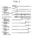
- Figs. 2A to 2J show operation timing charts of the respective constituent elements shown in Fig. 1.
- the battery 10 is a removable battery, for example.
- an AC/DC converter which converts AC power to DC power may be used to supply power to the power management IC 11, for example.
- the voltage at the input terminal of a voltage detector 20 of the power management IC 11 starts to increase gradually as shown in Fig. 2A.
- the voltage detector 20 monitors the voltage value supplied from the battery 10.
- the voltage detector 20 is held at its L (low) level until the voltage value from the battery 10 reaches a predetermined detected voltage value, and when the voltage value from the battery 10 reaches the predetermined detected voltage, the voltage detector 20 outputs a voltage detection signal which changes to its H (high) level.
- the voltage detection signal from the voltage detector 20 is sent to a counter 22.
- a first regulator 29 supplies the predetermined core voltage shown in Fig. 2C to the CPU 12.
- a clock generator 21 is a so-called RTC (real-time clock), and when the battery 10 is connected to the power management IC 11, the clock generator 21 starts a clock operation as shown in Fig. 2D.
- the clock signals outputted from the clock generator 21 are sent to the counter 22.
- the counter 22 starts to count the clock signals sent from the clock generator 21.
- the count signal outputted from the counter 22 is sent to each of a first comparator 26, a second comparator 27 and a third comparator 28.
- the first comparator 26 compares a count value M stored in a first MONOS (Metal-Oxide-Nitride-Oxide-Semiconductor) 23, which is a rewritable non-volatile memory, and the count value sent from the counter 22, and outputs a comparison detection signal which, as shown in Fig. 2F, is held at its L level until the count value from the counter 22 reaches the count value M of the first MONOS 23, and changes to its H level when the count value from the counter 22 reaches the count value M of the first MONOS 23.
- MONOS Metal-Oxide-Nitride-Oxide-Semiconductor
- the comparison detection signal of the first comparator 26 when the comparison detection signal of the first comparator 26 goes to the H level, the comparison detection signal of H level is sent to the CPU 12 as a reset release signal. In other words, in the preferred embodiment of the present invention, when the comparison detection signal of the first comparator 26 goes to the H level, reset release of the CPU 12 is performed.
- the second comparator 27 compares a count value N (N > M) stored in a second MONOS 24, which is a rewritable non-volatile memory, and the count value sent from the counter 22, and outputs a comparison detection signal which, as shown in Fig. 2G, is held at its L level until the count value from the counter 22 reaches the count value N of the second MONOS 24, and changes to its H level when the count value from the counter 22 reaches the count value N of the second MONOS 24.
- the comparison detection signal of the second comparator 27 goes to the H level, the comparison detection signal of H level is sent to a second regulator 30 as a power-on signal.
- the second regulator 30 When the power-on signal is supplied to the second regulator 30 from the second comparator 27 (when the comparison detection signal of the second comparator 27 goes to the H level), the second regulator 30 supplies I/O power of a predetermined voltage to the CPU 12 and the flash memory 13 as shown in Fig. 2H.
- the third comparator 28 compares a count value O (O > N) stored in a third MONOS 25, which is a rewritable non-volatile memory, and the count value sent from the counter 22, and outputs a comparison detection signal which, as shown in Fig. 2I, is held at its L level until the count value from the counter 22 reaches the count value O of the third MONOS 25, and changes to its H level when the count value from the counter 22 reaches the count value O of the third MONOS 25.
- the comparison detection signal of the third comparator 28 goes to the H level, the comparison detection signal of H level is sent to a third regulator 31 as a power-on signal.
- the third regulator 31 supplies I/O power of a predetermined voltage to the flash memory 13 as shown in Fig. 2J.
- each of the first MONOS 23, the second MONOS 24 and the third MONOS 25 is a non-volatile memory which data can be rewritten by injecting and ejecting electrons into and from the entire surface region under the gate electrode by tunnel current, or by using so-called hot carriers.
- the power management IC 11 according to the preferred embodiment of the present invention is configured so that the data of each of the first MONOS 23, the second MONOS 24 and the third MONOS 25 can be rewritten via a MONOS interface (I/F) 19.
- the timing of reset release of the CPU 12 can be changed to another desired timing.
- the count value N stored in the second MONOS 24 is rewritten into another desired value, the timing of I/O power supply to each of the CPU 12 and the flash memory 13 can be changed to another desired timing.
- the count value O stored in the third MONOS 25 is rewritten into another desired value, the timing of supply of core power to the flash memory 13 can be changed to another desired timing.
- the power management IC 11 in the power management IC 11 according to the preferred embodiment of the present invention, even if the specifications of the CPU 12 are modified and it is necessary to modify the timing of reset release of the CPU 12 and the timing of power-on of the corresponding ones of the regulators 29 to 31, or even if the specifications of the flash memory 13 are modified and it is necessary to modify the timing of power-on of the corresponding ones of the regulators 29 to 31, for example, it is possible to readily modify the timing of reset release of the CPU 12 and the timing of power-on of the regulators 29 to 31.
- the count values M, N and O which serve as comparison references in the respective first to third comparators 26 to 28 are stored in the first MONOS 23, second MONOS 24 and third MONOS 25, respectively.
- the counter setting values of a first variable counter, a second variable counter and a third variable counter may also be stored in the first MONOS 23, second MONOS 24 and third MONOS 25, respectively.
- the power management IC 11 may be configured so that the counter 22 shown in Fig.
- the first variable counter is configured to output a signal which goes to its H level when its count value reaches the count value M set by the first MONOS 23
- the second variable counter is configured to output a signal which goes to its H level when its count value reaches the count value N set by the second MONOS 24
- the third variable counter is configured to output a signal which goes to its H level when its count value reaches the count value O set by the third MONOS 25.
- the power management IC 11 can be applied to portable communications terminals and various other electronic apparatuses such as PDAs (Personal Digital Assistants) and digital cameras, portable and stationary television receivers, and personal computers, for example,.
- PDAs Personal Digital Assistants
- digital cameras Portable and stationary television receivers
- personal computers for example
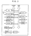
- Fig. 3 shows a main internal configuration of a portable communications terminal in which the power management IC 11 according to the present embodiment is incorporated.
- an antenna 41 is a built-in antenna, for example, and performs transmission and reception of radio wave signals.
- An RF block 43 is a communication circuit which performs wireless communication, and performs, for example, amplification and level adjustment of signals transmitted and received via the antenna 41, frequency conversion from RF to baseband, or frequency conversion from baseband to RF.
- a DSP (Digital Signal Processor) 47 performs modulation and demodulation of signals, spectrum spread and inverse spectrum spread, and a decision as to whether transmitted/received data are call voice data or data other than call voice data, for example.
- the data other than call voice data may be image data, electronic mails, program data and various other kinds of data.
- the received call voice data are sent to a codec 48 via a data line.
- the codec 48 decodes the call voice data, and sends the decoded voice data to a speaker 49 via the data line.
- the speaker 49 includes a digital/analog converter and an amplifier, and performs digital-to-analog conversion and amplification of the voice data and outputs the obtained voice data, thereby reproducing a call voice.
- the microphone 50 includes an analog/digital converter and an amplifier.
- a call voice signal inputted via this microphone 50 is amplified to a predetermined level by the amplifier and converted to digital voice data by the analog/digital converter.
- the digital voice data are sent to the codec 48 via the data line, and after having been encoded by the codec 48, are sent to the RF block 43 via the DSP 47.
- a memory 46 includes a ROM and a RAM.
- the ROM stores, for example, control programs and various initial setting values which are necessary for the CPU 12 to control each section, the telephone number of the portable communications terminal, font data, dictionary data, program codes for various applications, and identification information (ID) for the portable communications terminal.
- This ROM includes a rewritable ROM such as an EEPROM, and is also capable of storing telephone directories and electronic mail addresses which are set by a user, image data and ring tone data, character data, and various other user setting values.
- the flash memory 13 shown in Fig. 1 may be included in the ROM.
- the RAM serves as a work area during various kinds of data processing, and stores data as needed.
- a display section 44 includes, for example, a liquid crystal display and a drive circuit for displaying an image and the like on the display.
- An operation section 45 has various keys and a jog dial which are disposed on the case of the portable communications terminal, and a key operation signal generation section which generates an operation signal corresponding to the operation of each of the keys and the jog dial.
- the CPU 12 controls each constituent element of the portable communications terminal via a control line, and performs various arithmetic operations.
- the power management IC 11 has the configuration shown in Fig. 1 mentioned previously, and supplies power to each section from the battery 10.
- the portable communications terminal also includes a music recording and reproduction section for performing recording and reproduction of music, a browser function, an interface for providing connection between an external storage device such as an external memory and the terminal body, a connection terminal for an external remote controller, a short-distance wireless communication section for performing wireless communication (infrared communication and the like) of various kinds of information within a short distance, and a GPS (Global Positioning System) section which is a positioning device for detecting the current position of the portable communications terminal.
- a music recording and reproduction section for performing recording and reproduction of music
- a browser function an interface for providing connection between an external storage device such as an external memory and the terminal body
- a connection terminal for an external remote controller for an external remote controller
- a short-distance wireless communication section for performing wireless communication (infrared communication and the like) of various kinds of information within a short distance
- GPS Global Positioning System
- Fig. 4 shows essential constituent elements each of which power is to be supplied to from the power management IC 11 according to the preferred embodiment of the present invention, from among the constituent elements of the portable communications terminal which are shown in Fig. 3.
- a regulator 70 incorporated in the power management IC 11 includes a CPU core regulator 76 for supplying core power to the CPU 12 (the first regulator 29 shown in Fig. 1), a memory core regulator 77 for supplying core power to the memory 46 (the third regulator 31 shown in Fig. 1), an RF regulator 71 for supplying power to the RF block 43, an audio regulator 73 for supplying power to the codec 48, an LCD regulator 74 for supplying power to an LCD 61 of the display section 44, and a DSP core regulator 76 for supplying core power to the DSP 47.
- An I/O power supply regulator 72 (the second regulator 30 shown in Fig. 1) supplies I/O power not only to the CPU 12 and the memory 46 but also to the LCD 61 and the DSP 47.
- the power management IC 11 incorporated in the example shown in Fig. 4 includes MONOS's (not shown) each of which stores a value for setting the timing of power-on of a respective one of the regulators to the desired timing.
Landscapes
- Engineering & Computer Science (AREA)
- Theoretical Computer Science (AREA)
- Physics & Mathematics (AREA)
- General Engineering & Computer Science (AREA)
- General Physics & Mathematics (AREA)
- Power Sources (AREA)
- Mobile Radio Communication Systems (AREA)
- Charge And Discharge Circuits For Batteries Or The Like (AREA)
- Direct Current Feeding And Distribution (AREA)
Applications Claiming Priority (2)
| Application Number | Priority Date | Filing Date | Title |
|---|---|---|---|
| JP2004125833A JP2005309767A (ja) | 2004-04-21 | 2004-04-21 | 電源制御装置、電子機器、及び携帯電話端末 |
| JP2004125833 | 2004-04-21 |
Publications (2)
| Publication Number | Publication Date |
|---|---|
| EP1589402A2 true EP1589402A2 (de) | 2005-10-26 |
| EP1589402A3 EP1589402A3 (de) | 2007-07-04 |
Family
ID=34935557
Family Applications (1)
| Application Number | Title | Priority Date | Filing Date |
|---|---|---|---|
| EP05008793A Withdrawn EP1589402A3 (de) | 2004-04-21 | 2005-04-21 | Leistungregelvorrichtung, elektronisches Gerät, und tragbares Kommunkationsendgerät |
Country Status (5)
| Country | Link |
|---|---|
| US (1) | US7434077B2 (de) |
| EP (1) | EP1589402A3 (de) |
| JP (1) | JP2005309767A (de) |
| KR (1) | KR20060047357A (de) |
| CN (1) | CN100339795C (de) |
Families Citing this family (9)
| Publication number | Priority date | Publication date | Assignee | Title |
|---|---|---|---|---|
| US7627353B2 (en) * | 2007-03-01 | 2009-12-01 | Aerielle Technologies, Inc. | Circuit and method for providing an auto-off capability for a wireless transmitter |
| US7337342B1 (en) * | 2005-04-28 | 2008-02-26 | Summit Microelectronics, Inc. | Power supply sequencing distributed among multiple devices with linked operation |
| US7542445B2 (en) * | 2006-06-14 | 2009-06-02 | Sony Ericsson Mobile Communications Ab | Method and system for maintaining autonomous system clock accuracy for a mobile radio terminal |
| JP5173215B2 (ja) * | 2007-03-06 | 2013-04-03 | キヤノン株式会社 | 光学機器 |
| JP5107121B2 (ja) * | 2008-04-02 | 2012-12-26 | 株式会社リコー | データ転送装置及びその初期化方法、並びに画像形成装置 |
| JP2011114953A (ja) * | 2009-11-26 | 2011-06-09 | Seiko Instruments Inc | 通電時間計測回路及び電源装置 |
| JP5867173B2 (ja) * | 2012-03-05 | 2016-02-24 | 株式会社リコー | 電源起動制御装置 |
| CN104205002B (zh) * | 2012-03-30 | 2017-09-05 | 英特尔公司 | 用于传送可用电池电力的方法和装置 |
| US11385692B2 (en) * | 2019-11-27 | 2022-07-12 | Chao-Cheng Yu | Remote automatic control power supply system |
Citations (2)
| Publication number | Priority date | Publication date | Assignee | Title |
|---|---|---|---|---|
| EP0532790A1 (de) | 1991-09-16 | 1993-03-24 | Rohm Co., Ltd. | Ein-Chip-Mikrorechner |
| JPH0944468A (ja) | 1995-08-01 | 1997-02-14 | Denso Corp | 制御回路 |
Family Cites Families (10)
| Publication number | Priority date | Publication date | Assignee | Title |
|---|---|---|---|---|
| JPS62210521A (ja) | 1986-03-11 | 1987-09-16 | Fujitsu Ltd | リセツト処理方式 |
| JPH087742B2 (ja) | 1990-05-28 | 1996-01-29 | ローム株式会社 | ワンチップマイクロコンピュータ |
| US5530879A (en) * | 1994-09-07 | 1996-06-25 | International Business Machines Corporation | Computer system having power management processor for switching power supply from one state to another responsive to a closure of a switch, a detected ring or an expiration of a timer |
| JPH10105296A (ja) * | 1996-09-30 | 1998-04-24 | Casio Comput Co Ltd | 電源制御装置 |
| KR100253076B1 (ko) * | 1997-05-02 | 2000-05-01 | 윤종용 | 순차 로직들을 위한 파워-온 리셋 회로(power-on reset circuit for sequential logics) |
| US6173436B1 (en) * | 1997-10-24 | 2001-01-09 | Vlsi Technology, Inc. | Standard cell power-on-reset circuit |
| US6154821A (en) * | 1998-03-10 | 2000-11-28 | Rambus Inc. | Method and apparatus for initializing dynamic random access memory (DRAM) devices by levelizing a read domain |
| FR2788145B1 (fr) * | 1999-01-05 | 2001-08-17 | St Microelectronics Sa | Procede d'initialisation d'un microcontroleur |
| US6946753B2 (en) | 2002-11-14 | 2005-09-20 | Fyre Storm, Inc. | Switching power converter controller with watchdog timer |
| US7302600B2 (en) * | 2004-06-30 | 2007-11-27 | Marvell International Ltd. | Power supply detection method, apparatus, and system |
-
2004
- 2004-04-21 JP JP2004125833A patent/JP2005309767A/ja active Pending
-
2005
- 2005-04-18 US US11/107,803 patent/US7434077B2/en not_active Expired - Fee Related
- 2005-04-21 EP EP05008793A patent/EP1589402A3/de not_active Withdrawn
- 2005-04-21 CN CNB2005100656859A patent/CN100339795C/zh not_active Expired - Fee Related
- 2005-04-21 KR KR1020050033239A patent/KR20060047357A/ko not_active Ceased
Patent Citations (2)
| Publication number | Priority date | Publication date | Assignee | Title |
|---|---|---|---|---|
| EP0532790A1 (de) | 1991-09-16 | 1993-03-24 | Rohm Co., Ltd. | Ein-Chip-Mikrorechner |
| JPH0944468A (ja) | 1995-08-01 | 1997-02-14 | Denso Corp | 制御回路 |
Also Published As
| Publication number | Publication date |
|---|---|
| JP2005309767A (ja) | 2005-11-04 |
| CN100339795C (zh) | 2007-09-26 |
| KR20060047357A (ko) | 2006-05-18 |
| CN1690922A (zh) | 2005-11-02 |
| US7434077B2 (en) | 2008-10-07 |
| EP1589402A3 (de) | 2007-07-04 |
| US20050240789A1 (en) | 2005-10-27 |
Similar Documents
| Publication | Publication Date | Title |
|---|---|---|
| US6484041B1 (en) | Method for adjusting power consumption | |
| US7434077B2 (en) | Power control apparatus, electronic apparatus, and portable communications terminal | |
| KR20060121975A (ko) | 단일 라인상에 비휘발성 메모리 및 서미스터를 갖는 배터리회로 | |
| US6362605B1 (en) | Method and apparatus for providing power to an integrated circuit | |
| US20130159737A1 (en) | Universal Serial Bus Current Limit | |
| US7512821B2 (en) | Power supply system and method for supplying power to CPU providing power saving mode | |
| JP4131844B2 (ja) | 携帯端末 | |
| KR20040069512A (ko) | 전원제어 기능을 갖는 모바일 디바이스 및 모바일디바이스의 전원제어방법 | |
| US8249668B2 (en) | Communication device and power saving method thereof | |
| US7865168B2 (en) | Apparatus for controlling power consumption in PDA phone | |
| US7440773B2 (en) | Method for protecting user data in a personal digital assistant (PDA) telephone | |
| CA2509026C (en) | Universal serial bus current limit | |
| JP2000286930A (ja) | 携帯電話装置 | |
| CN115459374B (zh) | 无线耳机及其电路、充电盒及其电路、无线耳机组件 | |
| JP2010130755A (ja) | 保護回路及び電池パック並びに電子機器 | |
| KR100620745B1 (ko) | 배터리 잔류량 표시 기능을 가지는 전자기기 및 그 방법 | |
| JP2003018076A (ja) | 無線端末機 | |
| JP2000253593A (ja) | 携帯型無線電話装置とその電源制御方法 | |
| KR100706396B1 (ko) | 화면 밝기 조절 기능을 가지는 무선통신 단말기 및 그 방법 | |
| KR20030093878A (ko) | 절전기능을 갖는 휴대용 단말기 및 그 제어방법 | |
| KR101059841B1 (ko) | 이동통신 단말기에서 자동 파워 온을 위한 신호 지연 회로장치 | |
| JP2004096960A (ja) | 携帯機器のバックアップ電池充電回路 | |
| KR20010074405A (ko) | 내장된 충전 회로를 갖는 스마트 배터리 장치 및 그 제어방법 | |
| KR20050042835A (ko) | 비상전원을 이용하는 방법 및 이를 구현하는 이동통신단말기 | |
| EP0848317A2 (de) | Signalerzeugungsgerät und elektronisches Gerät dieses verwendend |
Legal Events
| Date | Code | Title | Description |
|---|---|---|---|
| PUAI | Public reference made under article 153(3) epc to a published international application that has entered the european phase |
Free format text: ORIGINAL CODE: 0009012 |
|
| AK | Designated contracting states |
Kind code of ref document: A2 Designated state(s): AT BE BG CH CY CZ DE DK EE ES FI FR GB GR HU IE IS IT LI LT LU MC NL PL PT RO SE SI SK TR |
|
| AX | Request for extension of the european patent |
Extension state: AL BA HR LV MK YU |
|
| PUAL | Search report despatched |
Free format text: ORIGINAL CODE: 0009013 |
|
| AK | Designated contracting states |
Kind code of ref document: A3 Designated state(s): AT BE BG CH CY CZ DE DK EE ES FI FR GB GR HU IE IS IT LI LT LU MC NL PL PT RO SE SI SK TR |
|
| AX | Request for extension of the european patent |
Extension state: AL BA HR LV MK YU |
|
| 17P | Request for examination filed |
Effective date: 20071204 |
|
| AKX | Designation fees paid |
Designated state(s): DE FR GB |
|
| 17Q | First examination report despatched |
Effective date: 20110406 |
|
| STAA | Information on the status of an ep patent application or granted ep patent |
Free format text: STATUS: THE APPLICATION IS DEEMED TO BE WITHDRAWN |
|
| 18D | Application deemed to be withdrawn |
Effective date: 20121101 |