EP1586004B1 - Platine oder substrat für ein organisches elektronikgerät, sowie verwendung dazu - Google Patents
Platine oder substrat für ein organisches elektronikgerät, sowie verwendung dazu Download PDFInfo
- Publication number
- EP1586004B1 EP1586004B1 EP03815039A EP03815039A EP1586004B1 EP 1586004 B1 EP1586004 B1 EP 1586004B1 EP 03815039 A EP03815039 A EP 03815039A EP 03815039 A EP03815039 A EP 03815039A EP 1586004 B1 EP1586004 B1 EP 1586004B1
- Authority
- EP
- European Patent Office
- Prior art keywords
- circuit board
- organic
- integrated
- display
- electronic device
- Prior art date
- Legal status (The legal status is an assumption and is not a legal conclusion. Google has not performed a legal analysis and makes no representation as to the accuracy of the status listed.)
- Expired - Lifetime
Links
Images


Classifications
-
- G—PHYSICS
- G06—COMPUTING OR CALCULATING; COUNTING
- G06K—GRAPHICAL DATA READING; PRESENTATION OF DATA; RECORD CARRIERS; HANDLING RECORD CARRIERS
- G06K19/00—Record carriers for use with machines and with at least a part designed to carry digital markings
- G06K19/06—Record carriers for use with machines and with at least a part designed to carry digital markings characterised by the kind of the digital marking, e.g. shape, nature, code
- G06K19/067—Record carriers with conductive marks, printed circuits or semiconductor circuit elements, e.g. credit or identity cards also with resonating or responding marks without active components
- G06K19/07—Record carriers with conductive marks, printed circuits or semiconductor circuit elements, e.g. credit or identity cards also with resonating or responding marks without active components with integrated circuit chips
- G06K19/077—Constructional details, e.g. mounting of circuits in the carrier
- G06K19/07701—Constructional details, e.g. mounting of circuits in the carrier the record carrier comprising an interface suitable for human interaction
- G06K19/07703—Constructional details, e.g. mounting of circuits in the carrier the record carrier comprising an interface suitable for human interaction the interface being visual
-
- G—PHYSICS
- G06—COMPUTING OR CALCULATING; COUNTING
- G06K—GRAPHICAL DATA READING; PRESENTATION OF DATA; RECORD CARRIERS; HANDLING RECORD CARRIERS
- G06K19/00—Record carriers for use with machines and with at least a part designed to carry digital markings
- G06K19/06—Record carriers for use with machines and with at least a part designed to carry digital markings characterised by the kind of the digital marking, e.g. shape, nature, code
- G06K19/067—Record carriers with conductive marks, printed circuits or semiconductor circuit elements, e.g. credit or identity cards also with resonating or responding marks without active components
- G06K19/07—Record carriers with conductive marks, printed circuits or semiconductor circuit elements, e.g. credit or identity cards also with resonating or responding marks without active components with integrated circuit chips
- G06K19/077—Constructional details, e.g. mounting of circuits in the carrier
-
- H—ELECTRICITY
- H01—ELECTRIC ELEMENTS
- H01L—SEMICONDUCTOR DEVICES NOT COVERED BY CLASS H10
- H01L2924/00—Indexing scheme for arrangements or methods for connecting or disconnecting semiconductor or solid-state bodies as covered by H01L24/00
- H01L2924/0001—Technical content checked by a classifier
- H01L2924/0002—Not covered by any one of groups H01L24/00, H01L24/00 and H01L2224/00
-
- H—ELECTRICITY
- H05—ELECTRIC TECHNIQUES NOT OTHERWISE PROVIDED FOR
- H05K—PRINTED CIRCUITS; CASINGS OR CONSTRUCTIONAL DETAILS OF ELECTRIC APPARATUS; MANUFACTURE OF ASSEMBLAGES OF ELECTRICAL COMPONENTS
- H05K1/00—Printed circuits
- H05K1/16—Printed circuits incorporating printed electric components, e.g. printed resistor, capacitor, inductor
Definitions
- the invention relates to a circuit board or a substrate for an electronic device, which is inexpensive to produce and can be easily integrated into the production process for organic electronics.
- the DE 199 35 527 A1 describes chip cards with display and a method for producing display elements with electronic control and drive lines for the display elements. It is described, the optical display elements as well as the electronic control components, possibly also a voltage source to arrange by means of organic semiconductor materials side by side on a plastic film.
- the DE 33 38 597 A1 discloses a multilayer data carrier in which a carrier element accommodating an IC module is installed, and a method for producing such a data carrier.
- organic-based active components such as transistors or passive components, such as resistors on substrates
- organic-based active components are known (not necessarily only of polymeric, but more generally of conductive, semiconducting, and insulating organic, ie, non-silicon-containing materials). preferably also flexible substrates to build.
- the electronics not based on the traditional semiconductors with silicon as a core element, but includes the organic semiconducting and conductive materials, it is necessary to provide the most affordable electronics available.
- the object of the present invention is therefore to provide a printed circuit board, a substrate or a base plate (all three terms stand for the same device) for an organic device which is intelligent or in which passive and / or active electronic components are integrated. This object is achieved by a circuit board according to claim 1.
- Active components are transistors, diodes, photocells, integrated circuits or the like. Furthermore, at least one active organic component in addition to at least one passive organic component is preferably integrated into the circuit board or the substrate. Passive components are resistors, coils and / or capacitors.
- Integrated is understood here as a contrast to the said hybrid structure.
- the integrated components are therefore not made extra and / or mounted in an extra step on the substrate, but the substrate is used according to the invention both as (conventional) board and to build the integrated electronics (therefore “smart board”).
- integrated also means, for example, applied to the surface, e.g. printed).
- the production of the entire electronic device takes place in a so-called thin-film process, (Organic thin functional layers that are inexpensive and easy to produce) and / or in a printing process, particularly preferably at least partially in the roll-to-roll process.
- a so-called thin-film process Organic thin functional layers that are inexpensive and easy to produce
- a printing process particularly preferably at least partially in the roll-to-roll process.
- the (total) power supply for the electronic device such as an energy converter, a photovoltaic cell, a piezoceramic element, an inductive coupling coil, a capacitive coupling antenna, can contact one another external power supply, a battery or similar integrated.
- an input element that is to say a sensor or a keyboard, as well as an output element, an antenna or the like can be integrated in the substrate or on the intelligent board.
- sensor for pressure, electrical current, electrical voltage, noise, temperature, humidity, pH, chemical compounds, gases, respiratory and / or blood alcohol, analysis of body fluids or aqueous starting materials in general
- Keyboard individual pushbuttons (simple connections or capacitively coupled pushbuttons or inductive pushbuttons), keyboard - keyboard, input matrix (eg touch screen)), microphone (sounds, noises), light sensor (also as detector or solar cell).
- optical elements light-emitting diodes (organic or inorganic), incandescent lamps, electrochromic elements (those which change their color or light absorption under the action of electric current / electrical voltage, Liquid crystal displays (LCD); Speakers (conventional or based on piezo-active materials (organic or inorganic)), antennas (inductively as coil or capacitive), electrical contacts for external contacting, screen (based on all possible principles such as conventional CRT screens, LCD (liquid crystal) displays, screens based on electrochromic materials, on so-called E-ink (name of an American company).
- optical elements light-emitting diodes (organic or inorganic), incandescent lamps, electrochromic elements (those which change their color or light absorption under the action of electric current / electrical voltage, Liquid crystal displays (LCD); Speakers (conventional or based on piezo-active materials (organic or inorganic)), antennas (inductively as coil or capacitive), electrical contacts for external contacting,
- Conventional wire or cable connections can be easily replaced by, for example, produced by printing, structured electrically conductive layers and / or conductor tracks.
- the substrate on which the active elements e.g. individual transistors or integrated circuits are constructed, at the same time serves as a circuit board and the necessary conductive connections (or resistors, coils or antennas) are applied directly to the same substrate with.
- the source / drain or gate electrode planes of the integrated circuits can be used over a large area for these printed conductors.
- Conductor tracks or conductive contacts can be realized for example by conductive adhesive.
- the substrate may be a flexible film, but it may be any other suitable material, almost any material.
- an inexpensive display which is based on the electrochromic effect
- an intelligent board or a substrate according to the invention wherein, for example, an electrochromic material is used as the display element and organic transistors are used as the drive circuit.
- the display can be pluggable or otherwise integrated, but it can also be considered as an independent component.
- the connections can be realized for example by a conductive adhesive. It is also possible to contactlessly transfer the data from an external device to the display (e.g., through a coil).
- a volatile or non-volatile memory may be integrated (organic or inorganic based).
- the color of a material is reversibly or irreversibly changed by applying an electrical voltage.
- an electrical voltage For example, you can change the color of the material PEDOT / PSS from almost clear to dark blue and PANI from green to blue.
- a second electrode is placed next to or above the electrochromic material and these two elements are connected by an electrolyte.
- a voltage between the two elements By applying a voltage between the two elements, a redox reaction takes place in the electrochromic material, which eventually leads to discoloration.
- a significant change in the electrical resistance of the materials takes place during this reaction.
- a control is needed, if it is not just a simple symbol, but as for example a 7-segment display or a matrix display is a variable display.
- This drive must receive the incoming signals e.g. connected by a NOR logic linked to the display so that the desired display appears.
- This control is advantageously constructed as an organic circuit based on organic field effect transistors whose function and structure are known.
- the display and the control electronics can for example be integrated in the same production step on the same substrate.
- the substrate is typically a low cost polymer film (e.g., PET, or PP, or PEN .. or polyimide).
- the display principle can be implemented very simply and inexpensively (for example, according to the publication of the Swedish Institute ACREO) This construction can also be carried out in the thin-film process and realized by printing processes, resulting in low cost and high numbers of displays for the first time.
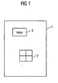
- FIG. 12 shows the area of the smart board or the substrate surface 1, where the substrate may be, for example, a flexible film, a cardboard, a flexible or a conventional glass substrate or the like. Externally visible are the input elements (keyboard, sensors, etc.) and the output elements 3 (display, display, light element, speaker). An opaque top surface hides the interior of the electronic device. The top surface can be designed or printed as desired.
- Each of the mentioned or usable electronic components may be organic, wherein organic and conventional, based on silicon based may be combined arbitrarily.
- FIG. 2 shows the structure of the smart board or the substrate according to the invention, wherein the layer below the opaque top surface ("the inner life") from FIG. 1 will be shown.
- the substrate 1 in addition to the visible input and output elements 2, 3, further elements 4, 5, 6 and, in between, electrical connections 7 are present.
- These elements 4 to 7 can either on the substrate 1 directly applied electronic
- elements integrated circuit, sensors, memory
- both the conductive compounds and the active electronic elements can be applied to the substrate.
- the invention can be used, for example, for the inexpensive production of greeting cards with small electronic games. In conventional greeting cards, in which when opening a small melody is played or the like, so far, the individual components are connected for example by wires. These compounds can be made much simpler according to the invention.
- FIG. 3 shows the top view of a 7 segment IPC display.
- an electrochromic display 9 and necessary control electronics 10 is applied based on organic transistors.
- contacts 11 are provided, which realize the electrical connection between the control electronics 10 and the display 9 via electrical connections 12.
- FIG. 4 Finally, it shows a cross section through the IPC display. In addition to the already in FIG. 3 elements described is still the protective layer 13 can be seen, which protects the system from external influences.
- electrochromic display for example, functional polymers such as PANI, PEDOT, or similar materials, for example macromolecules doped with chemical additives, are used.
- the invention makes it possible for the first time to integrate a printed circuit board as an active electronic component into an electronic device and to use it not only as a kind of base plate.
- an electronic device is created, which is not only much flatter and more compact, but an electronic device, the circuit board and even, depending on the embodiment, including display simple, inexpensive, so low-cost disposable product can be produced.
Landscapes
- Engineering & Computer Science (AREA)
- Computer Hardware Design (AREA)
- Microelectronics & Electronic Packaging (AREA)
- Physics & Mathematics (AREA)
- General Physics & Mathematics (AREA)
- Theoretical Computer Science (AREA)
- Thin Film Transistor (AREA)
- Devices For Indicating Variable Information By Combining Individual Elements (AREA)
Abstract
Description
- Die Erfindung betrifft eine Platine oder ein Substrat für ein elektronisches Gerät, die kostengünstig herstellbar ist und einfach in den Produktionsprozess für organische Elektronik integrierbar ist.
- Bekannt sind elektronische Bauteile, die auf sogenannten Platinen aufgebracht sind. Dabei werden einzelne aktive elektronische Elemente wie Transistoren, integrierte Schaltungen etc. auf die passive Platine gelötet und leitend entweder durch vorstrukturierte Leiterbahnen auf der Platine oder durch Kabelleitungen verbunden. Die einzelnen aktiven elektronischen Bauteile werden dabei alle extra gefertigt und in einem extra Arbeitsschritt auf die Platine montiert (Hybridaufbau). Bisher ist es nur möglich, passive Bauteile wie Widerstände oder Kondensatoren in solche Platinen zu integrieren, alle aktiven Teile werden wie beschrieben hybrid aufgebaut.
- Der nächste Stand der Technik, die
DE 199 35 527 A1 , beschreibt Chipkarten mit Display und ein Verfahren zum Herstellen von Anzeigeelementen mit elektronischer Ansteuerung und Ansteuerleitungen für die Anzeigeelemente. Dabei ist beschrieben, die optischen Anzeigeelemente als auch die elektronischen Ansteuerungsbestandteile, gegebenenfalls auch eine Spannungsquelle, mittels organischen Halbeitermaterialien nebeneinander auf einer Kunststofffolie anzuordnen. - Die
DE 33 38 597 A1 offenbart einen mehrschichtigen Datenträger, in welchen ein einen IC-Baustein aufnehmendes Trägerelement eingebaut ist, sowie ein Verfahren zur Herstellung eines solchen Datenträgers. - Bekannt ist in der organischen Elektronik, der sogenannten Polymerelektronik, organische basierte (nicht notwendigerweise nur aus polymeren, sondern allgemeiner gesehen aus leitfähigen, halbleitenden, und isolierenden organischen, also nicht Silizium enthaltenden Materialien) aktive Bauteile wie Transistoren oder passive Bauteile wie Widerstände auf Substraten, vorzugsweise auch flexiblen Substraten, aufzubauen.
- Zur Realisierung der sogenannten organischen Elektronik, der Elektronik die nicht auf den traditionellen Halbleitern mit Silizium als Kernelement aufbaut, sondern die organische halbleitende und leitende Materialien umfasst, ist es notwendig, eine möglichst preisgünstige Elektronik zur Verfügung zu stellen.
- Aufgabe der vorliegenden Erfindung ist es daher, eine Platine, ein Substrat oder eine Grundplatte (alle drei Begriffe stehen hier für dieselbe Vorrichtung) für ein organisches Gerät zu schaffen, die intelligent ist oder in die passive und/oder aktive elektronische Bauteile integriert sind. Diese Aufgabe wird gelöst durch eine Platine nach Anspruch 1.
- Aktive Bauteile sind dabei Transistoren, Dioden, Photozellen, integrierte Schaltungen oder ähnliches. Weiterhin ist in die Platine oder das Substrat vorzugsweise zumindest ein aktives organisches Bauteil neben zumindest einem passiven organischen Bauteil integriert. Passive Bauteile sind dabei Widerstände, Spulen und/oder Kondensatoren.
- "Integriert" versteht sich hier als Gegensatz zu dem genannten Hybridaufbau. Die integrierten Bauteile werden demnach nicht extra gefertigt und/oder in einem extra Arbeitsschritt auf das Substrat montiert, sondern das Substrat dient nach der Erfindung sowohl als (herkömmliche) Platine als auch zum Aufbau der integrierten Elektronik (deshalb "intelligente Platine"). "Integriert" heißt natürlich auch, dass es beispielsweise auf die Oberfläche aufgebracht, z.B. gedruckt ist).
- Für ein elektronisches Gerät wie ein Sensorlabel, ein Spiel, eine Checkkarte oder ein RFID Tag ist es wichtig, dass mehrere elektronisch verschiedene Bauteile oder Komponenten auf einer größeren Fläche elektrisch verbunden werden. Nachdem die (Herstellungs-)Kosten eine entscheidende Rolle in der organischen Elektronik spielen ist es wichtig, eine Möglichkeit der preisgünstigen Elektronik zu schaffen, mit deren Hilfe ganze Elektronikgeräte in einem Substrat integriert und damit in einem Prozess hergestellt werden können.
- Vorteilhafterweise erfolgt die Herstellung des gesamten elektronischen Geräts in einem sogenannten Dünnfilmprozess, (organische dünne Funktionsschichten, die preiswert und einfach herzustellen sind) und/oder in einem Druckprozess, insbesondere bevorzugt zumindest teilweise im roll-to-roll Prozess. Dadurch sind niedrige Kosten und hohe Stückzahlen realisierbar.
- Auf einem Substrat oder in einer intelligenten Platine nach der Erfindung kann die (gesamte) Energieversorgung für das elektronische Gerät, wie ein Energiewandler, eine photovoltaische Zelle, ein piezokeramisches Element, eine Spule zur induktiven Kopplung, eine Antenne zur kapazitiven Kopplung, einen Kontakt zu einer externen Stromversorgung, eine Batterie oder ähnliches integriert sein.
Ebenso kann ein Eingabeelement, also ein Sensor, oder eine Tastatur, sowie ein Ausgabeelement, eine Antenne oder sonstiges in dem Substrat oder auf der intelligenten Platine integriert sein. Folgende Bauteile werden hier beispielsweise als Eingabeelement bezeichnet: Sensor (für Druck, elektrischen Strom, elektrische Spannung, Geräusche, Temperatur, Feuchtigkeit, pH-Wert, chemische Verbindungen, Gase, Atem- und/oder Blutalkohol, Analyse von Körperflüssigkeiten oder von wässrigen Ausgangsmaterialien allgemein), Tastatur (einzelne Drucktasten (einfache Verbindungen oder kapazitiv gekoppelte Taster oder induktive Taster), keyboard - Tastatur, Eingabematrix (z.B. Touchscreen)), Mikrophon (Töne, Geräusche), Lichtsensor (auch als Detektor oder Solarzelle). - Folgende Bauteile werden beispielsweise als Ausgabeelemente bezeichnet: Optische Elemente (Leuchtdioden (organisch oder anorganisch), Glühlampen, elektrochrome Elemente (solche, die ihre Farbe oder Lichtabsorption unter Einwirkung von elektrischem Strom/elektrischer Spannung ändern, Flüssigkristall-Anzeigen (LCD); Lautsprecher (konventionelle oder auf piezoaktiven Materialien (organisch oder anorganisch) basierend), Antennen (induktiv als Spule oder kapazitiv), elektrische Kontakte für externe Kontaktierung, Bildschirm (basierend auf allen möglichen Prinzipien wie konventionelle Röhrenbildschirme, LCD (Flüssigkristall) - Anzeigen, Bildschirmen basierend auf elektrochromen Materialien, auf sog. E-ink (Name einer amerikanischen Firma).
- Herkömmliche Draht- oder Kabelverbindungen können einfach durch, beispielsweise drucktechnisch herstellbare, strukturierte elektrisch leitende Schichten und/oder Leiterbahnen ersetzt werden.
- Nach einer Ausführungsform ist vorgesehen, dass das Substrat auf dem die aktiven Elemente, z.B. einzelne Transistoren oder integrierte Schaltungen aufgebaut sind, gleichzeitig als Platine dient und die hierzu nötigen leitfähigen Verbindungen (oder Widerstände, Spulen oder Antennen) direkt auf dasselbe Substrat mit aufgebracht sind. Beispielsweise können die Source/Drain - oder Gate-Elektroden-Ebenen der integrierten Schaltungen großflächig für diese Leiterbahnen benutzt werden. Damit ist es auch möglich, hybride Aufbauten mit zu umfassen, beispielsweise eine Batterie, einen Taster oder Sensor und/oder einen Silizium-Chip an Stellen auf der intelligenten Platine oder dem Substrat an zu bringen. Leiterbahnen oder leitende Kontakte können beispielsweise auch durch leitfähigen Kleber realisiert sein.
- Das Substrat kann eine flexible Folie sein, es kann aber auch aus jedem anderen geeigneten Material, nahezu aus beliebigem Material sein.
- Des weiteren ist es möglich, ein preiswertes Display, das auf dem elektrochromen Effekt aufbaut, auf einer intelligenten Platine oder einem Substrat nach der Erfindung zu integrieren, wobei als Displayelement beispielsweise ein elektrochromes Material eingesetzt wird und als Ansteuerschaltung organische Transistoren verwendet werden. Dies ist insbesondere wirtschaftlich interessant, weil bislang Displays fast ausschließlich für hochpreisige Produkte eingesetzt werden.
- Das Display kann sowohl steckbar als auch anderweitig integriert werden, es kann aber auch als eigenständiges Bauteil betrachtet werden. Die Verbindungen können beispielsweise durch einen leitfähigen Kleber realisiert werden. Es ist auch eine kontaktlose Übertragung der Daten von einem externen Gerät auf das Display möglich (z.B. durch eine Spule).
- Auf dem Substrat können auch weitere Funktionen wie z.B. die Sensoreigenschaften Temperatur, Feuchtigkeit oder weitere logische Funktionen, vorzugsweise die Bauteile auf organischer Basis, aber nicht zwingend. Ebenso kann ein flüchtiger oder nichtflüchtiger Speicher integriert sein (organisch oder anorganisch basiert).
- Bei dem elektrochromen Effekt wird die Farbe eines Materials durch Anlegen einer elektrischen Spannung reversibel oder irreversibel verändert. Beispielsweise kann man bei dem Material PEDOT /PSS die Farbe von fast klar zu dunkelblau verändern und bei PANI von grün nach blau. Dies wird durch einen Aufbau realisiert, bei dem neben oder über dem elektrochromen Material eine zweite Elektrode plaziert wird und diese beiden Elemente durch einen Elektrolyten verbunden werden. Durch Anlegen einer Spannung zwischen den beiden Elementen findet eine Redox-Reaktion im elektrochromen Material statt, die schließlich zur Verfärbung führt. In der Regel findet bei dieser Reaktion auch eine deutliche Änderung des elektrischen Widerstandes der Materialien statt.
- Für solch ein Display wird eine Ansteuerung benötigt, wenn es sich nicht nur um ein einfaches Symbol handelt, sondern wie beispielsweise bei einem 7 Segment - display oder einem Matrix-Display um eine veränderbare Anzeige handelt. Diese Ansteuerung muss die eingehenden Signale z.B. durch eine NOR Logik so verknüpft zum Display leiten, dass die gewünschte Anzeige erscheint. Diese Ansteuerung ist vorteilhafterweise als organische Schaltung basierend auf organischen Feldeffekt Transistoren aufgebaut, deren Funktion und Aufbau bekannt sind.
- Das Display und die Ansteuerelektronik können beispielsweise im selben Produktionsschritt auf dasselbe Substrat integriert werden. Das Substrat ist typischerweise eine preiswerte Polymerfolie (z.B. PET, oder PP, oder PEN.. oder Polyimid). Das Displayprinzip kann sehr einfach und preiswert realisiert werden (z.B. nach der Veröffentlichung vom schwedischen Institut ACREO Auch dieser Aufbau kann im Dünnfilmprozess erfolgen und durch Druckprozesse realisiert werden. Hierdurch sind erstmals bei Displays auch niedrige Kosten und hohe Stückzahlen zu erzielen.
- Im folgenden wird die Erfindung noch anhand praktischer Beispiele, die Ausführungsformen zeigen, näher erläutert:
- Figur 1
- zeigt die Draufsicht auf ein elektronisches Gerät, das zumindest ein organisches Bauteil umfasst
- Figur 2
- zeigt die Draufsicht auf das gleiche elektronische organische Gerät, allerdings zeigt sie die unter dem Gehäuse befindliche Schicht.
- Figur 3
- zeigt die Draufsicht auf ein 7 Segment IPC-Display und
- Figur 4
- zeigt den Querschnitt durch ein IPC-Display.
-
Figur 1 zeigt die Fläche der intelligenten Platine oder die Substratfläche 1, wobei das Substrat beispielsweise eine flexible Folie, ein Karton, ein biegsames oder ein herkömmliches Glassubstrat oder ähnliches sein kann. Außen sichtbar sind die Eingabeelemente (Tastatur, Sensoren etc.) und die Ausgabeelemente 3 (Display, Anzeige, Leuchtelement, Lautsprecher). Durch eine undurchsichtige Deckfläche ist das Innenleben des elektronischen Gerätes verdeckt. Die Deckfläche kann beliebig gestaltet oder bedruckt sein. Jedes der genannten oder einsetzbaren elektronischen Bauteile kann organische sein, wobei auch organische und herkömmliche, auf Siliziumbasis beruhende beliebig kombiniert sein können. -
Figur 2 zeigt den Aufbau der intelligenten Platine oder des erfindungsgemäßen Substrats, wobei die Schicht unterhalb der undurchsichtigen Deckfläche ("das Innenleben") ausFigur 1 gezeigt wird. Hier erkennt man, dass auf dem Substrat 1, neben den sichtbaren Ein- und Ausgabeelementen 2,3 auch weitere Elemente 4,5,6 und dazwischen elektrischen Verbindungen 7 vorhanden sind. Diese Elemente 4 bis 7 können entweder auf dem Substrat 1 direkt aufgebrachte elektronische Elemente (integrierte Schaltung, Sensorik, Speicher) sein aber auch als Hybride aufgebrachte Elemente wie Batterien, Lautsprecher, konventionelle Elektronik, Speicher usw. sein. Nach der Erfindung können auf dem Substrat sowohl die leitenden Verbindungen als auch die aktiven Elektronikelemente aufgebracht sein. Damit kann die Erfindung beispielsweise auch zur preiswerten Herstellung von Grußkarten mit kleinen elektronischen Spielen eingesetzt werden. Bei herkömmlichen Grußkarten, bei denen beim Öffnen eine kleine Melodie abgespielt wird oder ähnliches, sind bisher die einzelnen Bauteile beispielsweise durch Drähte verbunden. Diese Verbindungen können nach der Erfindung wesentlich einfacher gestaltet werden. -
Figur 3 zeigt die Draufsicht auf ein 7 Segment IPC-Display. Auf einem flexiblen Substrat 8 ist ein electrochromes Display 9 sowie hierfür notwendige Ansteuerelektronik 10 basierend auf organischen Transistoren aufgebracht. Zur Kontaktierung des Displays sind Kontakte 11 vorgesehen, die über elektrische Verbindungen 12 die elektrische Verbindung zwischen der Ansteuerelektronik 10 und dem Display 9 realisieren. -
Figur 4 schließlich zeigt noch einen Querschnitt durch das IPC Display. Neben den bereits inFigur 3 beschriebenen Elementen ist noch die Schutzschicht 13 zu erkennen, die das System vor äußeren Einflüssen schützt. - Bei dem elektrochromen Display werden beispielsweise funktionale Polymere wie PANI, PEDOT, oder ähnliche Materialien, beispielsweise Makromoleküle, die durch chemische Zusätze dotiert wurden, eingesetzt.
- Durch die Erfindung ist es erstmals möglich, eine Platine als aktives elektronisches Bauelement in ein elektronisches Gerät mitzuintegrieren und sie nicht nur sozusagen als Grundplatte zu nutzen. Dadurch wird ein elektronisches Gerät geschaffen, das nicht nur wesentlich flacher und kompakter aufgebaut ist, sondern ein elektronisches Gerät, das inklusive Platine und sogar, je nach Ausführungsform, inklusive Display einfach, preiswert, also low-cost Einwegprodukt hergestellt werden kann.
Claims (11)
- Platine (1, 8) eines elektronischen Gerätes, wobei die Platine (1, 8) zumindest ein in die Platine (1, 8) integriertes aktives organisches elektronisches Bauteil umfasst, dadurch gekennzeichnet, dass zumindest eine Elektrodenschicht des integrierten aktiven organischen elektronischen Bauteils auch die Leiterbahnschicht zur Kontaktierung und Befestigung eines konventionellen siliziumbasierten Halbleiterbauelements auf der Platine ist
- Platine (1, 8) für ein elektronisches Gerät nach Anspruch 1,
dadurch gekennzeichnet, dass
in die Platine (1, 8) zumindest ein aktives organisches Bauteil neben zumindest einem passiven organischen Bauteil integriert ist. - Platine (1, 8) nach Anspruch 2, wobei das aktive Bauelement ein organischer Transistor, eine organische Diode, eine organische Photozelle, eine organische integrierte Schaltung und/oder das passive organische Bauteil eine elektrisch leitende Verbindung, ein Widerstand, eine Spule und/oder ein Kondensator ist.
- Platine (1, 8) nach einem der vorstehenden Ansprüche,
dadurch gekennzeichnet, dass
in die Platine (1, 8) eine Energieversorgung, also beispielsweise ein Energiewandler, eine photovoltaische Zelle, ein piezokeramisches Element, eine Spule zur induktiven Kopplung, eine Batterie oder Ähnliches integriert ist. - Platine (1, 8) nach einem der vorstehenden Ansprüche,
dadurch gekennzeichnet, dass
in die Platine (1, 8) ein Eingabeelement (2) und/oder ein Ausgabeelement (3) integriert ist. - Platine (1, 8) nach einem der vorstehenden Ansprüche,
dadurch gekennzeichnet, dass
Leitungen, wie Drahtleitungen oder leitende Kontakte durch strukturierte leitfähige Schichten, Elektroden wie die Source und Drain Elektroden und/oder leitfähigen Kleber realisiert sind. - Platine (1, 8) nach einem der vorstehenden Ansprüche
dadurch gekennzeichnet, dass
in die Platine (1, 8) ein Anzeigeelement und/oder ein Display (9) integriert ist. - Platine (1, 8) nach Anspruch 7,
dadurch gekennzeichnet, dass
das Display (9) elektrochromes Material, flüssigkristalline Elemente und/oder organische Leuchtdioden umfasst. - Platine (1, 8) nach Anspruch 7 oder 8,
dadurch gekennzeichnet, dass
in die Platine (1, 8) eine zu dem Display (9) gehörige Ansteuerelektronik (10) integriert ist. - Platine (1, 8) nach Anspruch 9,
dadurch gekennzeichnet, dass
die Ansteuerelektronik(10) zumindest einen organischen Feldeffekt-Transistor umfasst. - Verwendung einer Platine nach einem der Ansprüche 1 bis 10 für ein elektronisches Gerät wie ein Sensorlabel, ein Werbeetikett, ein Preisschild, ein Spiel, eine Checkkarte und/oder einen RFID Tag.
Applications Claiming Priority (3)
| Application Number | Priority Date | Filing Date | Title |
|---|---|---|---|
| DE10300519 | 2003-01-09 | ||
| DE10300519 | 2003-01-09 | ||
| PCT/DE2003/004151 WO2004063806A1 (de) | 2003-01-09 | 2003-12-16 | Platine oder substrat für ein organisches elektronikgerät, sowie verwendung dazu |
Publications (2)
| Publication Number | Publication Date |
|---|---|
| EP1586004A1 EP1586004A1 (de) | 2005-10-19 |
| EP1586004B1 true EP1586004B1 (de) | 2011-01-26 |
Family
ID=32694878
Family Applications (1)
| Application Number | Title | Priority Date | Filing Date |
|---|---|---|---|
| EP03815039A Expired - Lifetime EP1586004B1 (de) | 2003-01-09 | 2003-12-16 | Platine oder substrat für ein organisches elektronikgerät, sowie verwendung dazu |
Country Status (4)
| Country | Link |
|---|---|
| US (1) | US20060125061A1 (de) |
| EP (1) | EP1586004B1 (de) |
| DE (1) | DE50313445D1 (de) |
| WO (1) | WO2004063806A1 (de) |
Cited By (1)
| Publication number | Priority date | Publication date | Assignee | Title |
|---|---|---|---|---|
| DE102015010458A1 (de) * | 2015-08-11 | 2017-02-16 | Giesecke & Devrient Gmbh | Tragbarer Datenträger, inbesondere Chipkarte |
Families Citing this family (10)
| Publication number | Priority date | Publication date | Assignee | Title |
|---|---|---|---|---|
| DE102005017655B4 (de) * | 2005-04-15 | 2008-12-11 | Polyic Gmbh & Co. Kg | Mehrschichtiger Verbundkörper mit elektronischer Funktion |
| DE102005034351A1 (de) * | 2005-07-22 | 2007-01-25 | Sension, Biologische Detektions- Und Schnelltestsysteme Gmbh | Farb-Umschlag-Indikator zur Statusanzeige von RFID-Tickets und -Etiketten |
| DE102006001854A1 (de) * | 2006-01-13 | 2007-07-26 | Siemens Ag | Display mit Energiespeicher, sowie Herstellungsverfahren dazu |
| DE102007043920A1 (de) | 2007-07-17 | 2009-01-22 | Merck Patent Gmbh | Funktionelles Material für gedruckte elektronische Bauteile |
| US20090107018A1 (en) * | 2007-08-27 | 2009-04-30 | Richard Schmelzer | Systems and methods for display or collection of decorative accessories |
| CN101377983B (zh) * | 2007-08-29 | 2012-03-14 | 博西华电器(江苏)有限公司 | 家用电器操作装置和指示单元操作方法 |
| GB2457666B (en) * | 2008-02-19 | 2012-09-12 | Dw Spinks Embossing Ltd | Thin film display |
| DE102009004491A1 (de) | 2009-01-09 | 2010-07-15 | Merck Patent Gmbh | Funktionelles Material für gedruckte elektronische Bauteile |
| DE102018010197A1 (de) * | 2018-12-18 | 2020-06-18 | GRID INVENT gGmbH | Elektronisches Element und elektrisch angesteuertes Anzeigeelement |
| DE102020002046A1 (de) | 2020-03-31 | 2021-09-30 | Mike Rost | Vorrichtung zum Anzeigen veränderlicher Bilder auf der Oberfläche des Gehäuses von Mobilgeräten |
Family Cites Families (47)
| Publication number | Priority date | Publication date | Assignee | Title |
|---|---|---|---|---|
| US4246298A (en) * | 1979-03-14 | 1981-01-20 | American Can Company | Rapid curing of epoxy resin coating compositions by combination of photoinitiation and controlled heat application |
| US4340057A (en) * | 1980-12-24 | 1982-07-20 | S. C. Johnson & Son, Inc. | Radiation induced graft polymerization |
| DE3338597A1 (de) * | 1983-10-24 | 1985-05-02 | GAO Gesellschaft für Automation und Organisation mbH, 8000 München | Datentraeger mit integriertem schaltkreis und verfahren zur herstellung desselben |
| US4554229A (en) * | 1984-04-06 | 1985-11-19 | At&T Technologies, Inc. | Multilayer hybrid integrated circuit |
| GB2215307B (en) * | 1988-03-04 | 1991-10-09 | Unisys Corp | Electronic component transportation container |
| US5364735A (en) * | 1988-07-01 | 1994-11-15 | Sony Corporation | Multiple layer optical record medium with protective layers and method for producing same |
| US4937119A (en) * | 1988-12-15 | 1990-06-26 | Hoechst Celanese Corp. | Textured organic optical data storage media and methods of preparation |
| US5892244A (en) * | 1989-01-10 | 1999-04-06 | Mitsubishi Denki Kabushiki Kaisha | Field effect transistor including πconjugate polymer and liquid crystal display including the field effect transistor |
| FR2644920B1 (fr) * | 1989-03-21 | 1993-09-24 | France Etat | Dispositif d'affichage polychrome a memoire du type photoconducteur-electroluminescent |
| FI84862C (fi) * | 1989-08-11 | 1992-01-27 | Vaisala Oy | Kapacitiv fuktighetsgivarkonstruktion och foerfarande foer framstaellning daerav. |
| JPH0722669A (ja) * | 1993-07-01 | 1995-01-24 | Mitsubishi Electric Corp | 可塑性機能素子 |
| EP1257134A3 (de) * | 1994-02-24 | 2003-02-12 | Gte Mobile Communications Service Corporation | Zellulares Funktelefonsystem mit fernprogrammierbaren Mobilstationen |
| JP3246189B2 (ja) * | 1994-06-28 | 2002-01-15 | 株式会社日立製作所 | 半導体表示装置 |
| US5625199A (en) * | 1996-01-16 | 1997-04-29 | Lucent Technologies Inc. | Article comprising complementary circuit with inorganic n-channel and organic p-channel thin film transistors |
| JP3080579B2 (ja) * | 1996-03-06 | 2000-08-28 | 富士機工電子株式会社 | エアリア・グリッド・アレイ・パッケージの製造方法 |
| US6566156B1 (en) * | 1996-06-12 | 2003-05-20 | The Trustees Of Princeton University | Patterning of thin films for the fabrication of organic multi-color displays |
| US5693956A (en) * | 1996-07-29 | 1997-12-02 | Motorola | Inverted oleds on hard plastic substrate |
| US6344662B1 (en) * | 1997-03-25 | 2002-02-05 | International Business Machines Corporation | Thin-film field-effect transistor with organic-inorganic hybrid semiconductor requiring low operating voltages |
| US5998805A (en) * | 1997-12-11 | 1999-12-07 | Motorola, Inc. | Active matrix OED array with improved OED cathode |
| DE69918308T2 (de) * | 1998-04-10 | 2004-10-21 | E Ink Corp | Elektronische anzeige basierend auf organischen feldeffekt-transistoren |
| GB9808061D0 (en) * | 1998-04-16 | 1998-06-17 | Cambridge Display Tech Ltd | Polymer devices |
| TW410478B (en) * | 1998-05-29 | 2000-11-01 | Lucent Technologies Inc | Thin-film transistor monolithically integrated with an organic light-emitting diode |
| DK1956365T3 (da) * | 1998-08-26 | 2013-03-11 | Senseonics Inc | Optisk-baserede sensor-indretninger |
| US6384804B1 (en) * | 1998-11-25 | 2002-05-07 | Lucent Techonologies Inc. | Display comprising organic smart pixels |
| US6506438B2 (en) * | 1998-12-15 | 2003-01-14 | E Ink Corporation | Method for printing of transistor arrays on plastic substrates |
| US6114088A (en) * | 1999-01-15 | 2000-09-05 | 3M Innovative Properties Company | Thermal transfer element for forming multilayer devices |
| WO2000041893A1 (en) * | 1999-01-15 | 2000-07-20 | 3M Innovative Properties Company | Thermal transfer element and process for forming organic electroluminescent devices |
| US6180956B1 (en) * | 1999-03-03 | 2001-01-30 | International Business Machine Corp. | Thin film transistors with organic-inorganic hybrid materials as semiconducting channels |
| US6498114B1 (en) * | 1999-04-09 | 2002-12-24 | E Ink Corporation | Method for forming a patterned semiconductor film |
| JP4136185B2 (ja) * | 1999-05-12 | 2008-08-20 | パイオニア株式会社 | 有機エレクトロルミネッセンス多色ディスプレイ及びその製造方法 |
| US6366017B1 (en) * | 1999-07-14 | 2002-04-02 | Agilent Technologies, Inc/ | Organic light emitting diodes with distributed bragg reflector |
| DE19935527A1 (de) * | 1999-07-28 | 2001-02-08 | Giesecke & Devrient Gmbh | Aktive Folie für Chipkarten mit Display |
| US6593690B1 (en) * | 1999-09-03 | 2003-07-15 | 3M Innovative Properties Company | Large area organic electronic devices having conducting polymer buffer layers and methods of making same |
| JP4595143B2 (ja) * | 1999-09-06 | 2010-12-08 | 双葉電子工業株式会社 | 有機elデバイスとその製造方法 |
| EP1085320A1 (de) * | 1999-09-13 | 2001-03-21 | Interuniversitair Micro-Elektronica Centrum Vzw | Vorrichtung auf Basis von organischem Material zur Erfassung eines Probenanalyts |
| EP1149420B1 (de) * | 1999-10-11 | 2015-03-04 | Creator Technology B.V. | Integrierter schaltkreis |
| US6621098B1 (en) * | 1999-11-29 | 2003-09-16 | The Penn State Research Foundation | Thin-film transistor and methods of manufacturing and incorporating a semiconducting organic material |
| US6197663B1 (en) * | 1999-12-07 | 2001-03-06 | Lucent Technologies Inc. | Process for fabricating integrated circuit devices having thin film transistors |
| JP2002162652A (ja) * | 2000-01-31 | 2002-06-07 | Fujitsu Ltd | シート状表示装置、樹脂球状体、及びマイクロカプセル |
| TW497120B (en) * | 2000-03-06 | 2002-08-01 | Toshiba Corp | Transistor, semiconductor device and manufacturing method of semiconductor device |
| US6329226B1 (en) * | 2000-06-01 | 2001-12-11 | Agere Systems Guardian Corp. | Method for fabricating a thin-film transistor |
| DE10033112C2 (de) * | 2000-07-07 | 2002-11-14 | Siemens Ag | Verfahren zur Herstellung und Strukturierung organischer Feldeffekt-Transistoren (OFET), hiernach gefertigter OFET und seine Verwendung |
| DE10120687A1 (de) * | 2001-04-27 | 2002-10-31 | Siemens Ag | Verkapseltes organisch-elektronisches Bauteil, Verfahren zu seiner Herstellung und seine Verwendung |
| DE10043204A1 (de) * | 2000-09-01 | 2002-04-04 | Siemens Ag | Organischer Feld-Effekt-Transistor, Verfahren zur Strukturierung eines OFETs und integrierte Schaltung |
| US6699728B2 (en) * | 2000-09-06 | 2004-03-02 | Osram Opto Semiconductors Gmbh | Patterning of electrodes in oled devices |
| DE10045192A1 (de) * | 2000-09-13 | 2002-04-04 | Siemens Ag | Organischer Datenspeicher, RFID-Tag mit organischem Datenspeicher, Verwendung eines organischen Datenspeichers |
| DE10047171A1 (de) * | 2000-09-22 | 2002-04-18 | Siemens Ag | Elektrode und/oder Leiterbahn für organische Bauelemente und Herstellungverfahren dazu |
-
2003
- 2003-12-16 US US10/541,956 patent/US20060125061A1/en not_active Abandoned
- 2003-12-16 WO PCT/DE2003/004151 patent/WO2004063806A1/de not_active Ceased
- 2003-12-16 DE DE50313445T patent/DE50313445D1/de not_active Expired - Lifetime
- 2003-12-16 EP EP03815039A patent/EP1586004B1/de not_active Expired - Lifetime
Cited By (1)
| Publication number | Priority date | Publication date | Assignee | Title |
|---|---|---|---|---|
| DE102015010458A1 (de) * | 2015-08-11 | 2017-02-16 | Giesecke & Devrient Gmbh | Tragbarer Datenträger, inbesondere Chipkarte |
Also Published As
| Publication number | Publication date |
|---|---|
| DE50313445D1 (de) | 2011-03-10 |
| WO2004063806A1 (de) | 2004-07-29 |
| US20060125061A1 (en) | 2006-06-15 |
| EP1586004A1 (de) | 2005-10-19 |
Similar Documents
| Publication | Publication Date | Title |
|---|---|---|
| Tan et al. | Solution-processable, soft, self-adhesive, and conductive polymer composites for soft electronics | |
| EP1586004B1 (de) | Platine oder substrat für ein organisches elektronikgerät, sowie verwendung dazu | |
| TWI431804B (zh) | 製造可定址及靜態電子顯示器、發電或其它電子裝置之方法 | |
| EP3264239A1 (de) | Integrierter berührunsgsensor und anzeigevorrichtung mit fingerabdrucksensor sowie drucksensor | |
| EP1828963B1 (de) | Erkennungssystem | |
| EP2565829B1 (de) | Sicherheits- und/oder Wertdokument | |
| EP1328943A1 (de) | Organischer datenspeicher, identifizierungsmarke (rfid-tag) mit organischem datenspeicher, verwendungen eines organischen datenspeichers | |
| Lamport et al. | Organic thin film transistors in mechanical sensors | |
| DE19805282A1 (de) | Flächiger Träger mit einer Anzeigeeinrichtung | |
| DE102012203251A1 (de) | Kontaktlose Datenübertragungseinrichtung, diese enthaltendes Sicherheits- bzw. Wertdokument | |
| CN106095204B (zh) | 触摸传感器装置 | |
| CN102445808A (zh) | 透明基板点阵型电泳显示器及其制造方法 | |
| CN116113285A (zh) | 一种显示面板及其制备方法、显示模组 | |
| DE10214371A1 (de) | Wert- oder Sicherheitsdokument mit einer Schaltung | |
| DE112020005544T5 (de) | Anzeigefeld und Anzeigegerät | |
| CN106095176A (zh) | 一种镀铜纳米银线触摸屏及其制造方法 | |
| US20070051940A1 (en) | Device and method for determining the physical condition of an animal | |
| EP1801879A3 (de) | Elektronisches Gerät mit eindeutiger Kodierung | |
| CN202351593U (zh) | 玻璃基板笔段型电子纸显示器 | |
| Alessio et al. | Nanostructured Thin Films Enhancing the Performance of New Organic Electronic Devices: Does It Make Sense? | |
| CN102982776B (zh) | 利用线路板节省旁路电容的方法 | |
| DE102006001487A1 (de) | Elektrisch steuerbare Anzeigevorrichung mit elektrisch beheizbarer thermochromer Schicht | |
| DE102004054622A1 (de) | Schichtanordnung für eine Leiterplatte | |
| JP2008033094A (ja) | 表示装置 | |
| DE102019104385B4 (de) | Sensorsubstrat mit Elektronik sowie Verwendung dazu |
Legal Events
| Date | Code | Title | Description |
|---|---|---|---|
| PUAI | Public reference made under article 153(3) epc to a published international application that has entered the european phase |
Free format text: ORIGINAL CODE: 0009012 |
|
| 17P | Request for examination filed |
Effective date: 20050706 |
|
| AK | Designated contracting states |
Kind code of ref document: A1 Designated state(s): AT BE BG CH CY CZ DE DK EE ES FI FR GB GR HU IE IT LI LU MC NL PT RO SE SI SK TR |
|
| RAP1 | Party data changed (applicant data changed or rights of an application transferred) |
Owner name: POLYIC GMBH & CO. KG |
|
| RBV | Designated contracting states (corrected) |
Designated state(s): DE ES FR GB IT |
|
| RAP1 | Party data changed (applicant data changed or rights of an application transferred) |
Owner name: POLYIC GMBH & CO. KG |
|
| GRAP | Despatch of communication of intention to grant a patent |
Free format text: ORIGINAL CODE: EPIDOSNIGR1 |
|
| GRAS | Grant fee paid |
Free format text: ORIGINAL CODE: EPIDOSNIGR3 |
|
| GRAA | (expected) grant |
Free format text: ORIGINAL CODE: 0009210 |
|
| AK | Designated contracting states |
Kind code of ref document: B1 Designated state(s): DE ES FR GB IT |
|
| REG | Reference to a national code |
Ref country code: GB Ref legal event code: FG4D Free format text: NOT ENGLISH |
|
| REF | Corresponds to: |
Ref document number: 50313445 Country of ref document: DE Date of ref document: 20110310 Kind code of ref document: P |
|
| REG | Reference to a national code |
Ref country code: DE Ref legal event code: R096 Ref document number: 50313445 Country of ref document: DE Effective date: 20110310 |
|
| PG25 | Lapsed in a contracting state [announced via postgrant information from national office to epo] |
Ref country code: ES Free format text: LAPSE BECAUSE OF FAILURE TO SUBMIT A TRANSLATION OF THE DESCRIPTION OR TO PAY THE FEE WITHIN THE PRESCRIBED TIME-LIMIT Effective date: 20110507 |
|
| PLBE | No opposition filed within time limit |
Free format text: ORIGINAL CODE: 0009261 |
|
| STAA | Information on the status of an ep patent application or granted ep patent |
Free format text: STATUS: NO OPPOSITION FILED WITHIN TIME LIMIT |
|
| 26N | No opposition filed |
Effective date: 20111027 |
|
| REG | Reference to a national code |
Ref country code: DE Ref legal event code: R097 Ref document number: 50313445 Country of ref document: DE Effective date: 20111027 |
|
| PG25 | Lapsed in a contracting state [announced via postgrant information from national office to epo] |
Ref country code: IT Free format text: LAPSE BECAUSE OF FAILURE TO SUBMIT A TRANSLATION OF THE DESCRIPTION OR TO PAY THE FEE WITHIN THE PRESCRIBED TIME-LIMIT Effective date: 20110126 |
|
| PGFP | Annual fee paid to national office [announced via postgrant information from national office to epo] |
Ref country code: GB Payment date: 20131217 Year of fee payment: 11 Ref country code: DE Payment date: 20131127 Year of fee payment: 11 |
|
| PGFP | Annual fee paid to national office [announced via postgrant information from national office to epo] |
Ref country code: FR Payment date: 20131213 Year of fee payment: 11 |
|
| REG | Reference to a national code |
Ref country code: DE Ref legal event code: R119 Ref document number: 50313445 Country of ref document: DE |
|
| GBPC | Gb: european patent ceased through non-payment of renewal fee |
Effective date: 20141216 |
|
| REG | Reference to a national code |
Ref country code: FR Ref legal event code: ST Effective date: 20150831 |
|
| PG25 | Lapsed in a contracting state [announced via postgrant information from national office to epo] |
Ref country code: GB Free format text: LAPSE BECAUSE OF NON-PAYMENT OF DUE FEES Effective date: 20141216 Ref country code: DE Free format text: LAPSE BECAUSE OF NON-PAYMENT OF DUE FEES Effective date: 20150701 |
|
| PG25 | Lapsed in a contracting state [announced via postgrant information from national office to epo] |
Ref country code: FR Free format text: LAPSE BECAUSE OF NON-PAYMENT OF DUE FEES Effective date: 20141231 |