EP1583137B1 - Substrat-Meniskus-Schnittstelle und Verfahren zum Betreiben - Google Patents
Substrat-Meniskus-Schnittstelle und Verfahren zum Betreiben Download PDFInfo
- Publication number
- EP1583137B1 EP1583137B1 EP05251903A EP05251903A EP1583137B1 EP 1583137 B1 EP1583137 B1 EP 1583137B1 EP 05251903 A EP05251903 A EP 05251903A EP 05251903 A EP05251903 A EP 05251903A EP 1583137 B1 EP1583137 B1 EP 1583137B1
- Authority
- EP
- European Patent Office
- Prior art keywords
- wafer
- substrate
- processing
- fluid
- docking station
- Prior art date
- Legal status (The legal status is an assumption and is not a legal conclusion. Google has not performed a legal analysis and makes no representation as to the accuracy of the status listed.)
- Expired - Lifetime
Links
Images


Classifications
-
- H—ELECTRICITY
- H10—SEMICONDUCTOR DEVICES; ELECTRIC SOLID-STATE DEVICES NOT OTHERWISE PROVIDED FOR
- H10P—GENERIC PROCESSES OR APPARATUS FOR THE MANUFACTURE OR TREATMENT OF DEVICES COVERED BY CLASS H10
- H10P52/00—Grinding, lapping or polishing of wafers, substrates or parts of devices
-
- H—ELECTRICITY
- H10—SEMICONDUCTOR DEVICES; ELECTRIC SOLID-STATE DEVICES NOT OTHERWISE PROVIDED FOR
- H10P—GENERIC PROCESSES OR APPARATUS FOR THE MANUFACTURE OR TREATMENT OF DEVICES COVERED BY CLASS H10
- H10P72/00—Handling or holding of wafers, substrates or devices during manufacture or treatment thereof
- H10P72/04—Apparatus for manufacture or treatment
- H10P72/0402—Apparatus for fluid treatment
- H10P72/0406—Apparatus for fluid treatment for cleaning followed by drying, rinsing, stripping, blasting or the like
- H10P72/0411—Apparatus for fluid treatment for cleaning followed by drying, rinsing, stripping, blasting or the like for wet cleaning or washing
- H10P72/0414—Apparatus for fluid treatment for cleaning followed by drying, rinsing, stripping, blasting or the like for wet cleaning or washing using mainly spraying means, e.g. nozzles
-
- H—ELECTRICITY
- H10—SEMICONDUCTOR DEVICES; ELECTRIC SOLID-STATE DEVICES NOT OTHERWISE PROVIDED FOR
- H10P—GENERIC PROCESSES OR APPARATUS FOR THE MANUFACTURE OR TREATMENT OF DEVICES COVERED BY CLASS H10
- H10P72/00—Handling or holding of wafers, substrates or devices during manufacture or treatment thereof
- H10P72/04—Apparatus for manufacture or treatment
- H10P72/0402—Apparatus for fluid treatment
- H10P72/0406—Apparatus for fluid treatment for cleaning followed by drying, rinsing, stripping, blasting or the like
- H10P72/0408—Apparatus for fluid treatment for cleaning followed by drying, rinsing, stripping, blasting or the like for drying
-
- Y—GENERAL TAGGING OF NEW TECHNOLOGICAL DEVELOPMENTS; GENERAL TAGGING OF CROSS-SECTIONAL TECHNOLOGIES SPANNING OVER SEVERAL SECTIONS OF THE IPC; TECHNICAL SUBJECTS COVERED BY FORMER USPC CROSS-REFERENCE ART COLLECTIONS [XRACs] AND DIGESTS
- Y10—TECHNICAL SUBJECTS COVERED BY FORMER USPC
- Y10S—TECHNICAL SUBJECTS COVERED BY FORMER USPC CROSS-REFERENCE ART COLLECTIONS [XRACs] AND DIGESTS
- Y10S134/00—Cleaning and liquid contact with solids
- Y10S134/902—Semiconductor wafer
Definitions
- the present invention relates to semiconductor wafer processing and, more particularly, to apparatuses and techniques for more efficiently applying and removing fluids from wafer surfaces while reducing contamination and decreasing wafer cleaning cost.
- wafer cleaning may have to be conducted where a fabrication operation has been performed that leaves unwanted residues on the surfaces of wafers.
- a fabrication operation examples include plasma etching (e.g. , tungsten etch back (WEB)) and chemical mechanical polishing (CMP).
- plasma etching e.g. , tungsten etch back (WEB)
- CMP chemical mechanical polishing
- a wafer is placed in a holder which pushes a wafer surface against a rolling belt polisher.
- This belt polisher uses a slurry which consists of chemicals and abrasive materials to cause the polishing.
- this process tends to leave an accumulation of slurry particles and residues at the wafer surface.
- the unwanted residual material and particles may cause, among other things, defects such as scratches on the wafer surface and inappropriate interactions between metallization features. In some cases, such defects may cause devices on the wafer to become inoperable. In order to avoid the undue costs of discarding wafers having inoperable devices, it is therefore necessary to clean the wafer adequately yet efficiently after fabrication operations that leave unwanted residues.
- the wafer After a wafer has been wet cleaned, the wafer must be dried effectively to prevent water or cleaning fluid remnants from leaving residues on the wafer. If the cleaning fluid on the wafer surface is allowed to evaporate, as usually happens when droplets form, residues or contaminants previously dissolved in the cleaning fluid will remain on the wafer surface after evaporation (e.g., and form spots). To prevent evaporation from taking place, the cleaning fluid must be removed as quickly as possible without the formation of droplets on the wafer surface. In an attempt to accomplish this, one of several different drying techniques are employed such as spin drying, IPA, or Marangoni drying.
- FIG. 1 illustrates movement of cleaning fluids on a wafer 10 during an SRD drying process.
- a wet wafer is rotated at a high rate by rotation 14.
- the water or cleaning fluid used to clean the wafer is pulled from the center of the wafer to the outside of the wafer and finally off of the wafer as shown by fluid directional arrows 16.
- a moving liquid/gas interface 12 is created at the center of the wafer and moves to the outside of the wafer (i.e. , the circle produced by the moving liquid/gas interface 12 gets larger) as the drying process progresses.
- the inside area of the circle formed by the moving liquid/gas interface 12 is free from the fluid and the outside area of the circle formed by the moving liquid/gas interface 12 is the cleaning fluid. Therefore, as the drying process continues, the section inside (the dry area) of the moving liquid/gas interface 12 increases while the area (the wet area) outside of the moving liquid/gas interface 12 decreases. As stated previously, if the moving liquid/gas interface 12 breaks down, droplets of the cleaning fluid form on the wafer and contamination may occur due to evaporation of the droplets. As such, it is imperative that droplet formation and the subsequent evaporation be limited to keep contaminants off of the wafer surface. Unfortunately, the present drying methods are only partially successful at the prevention of moving liquid interface breakdown.
- the SRD process has difficulties with drying wafer surfaces that are hydrophobic. Hydrophobic wafer surfaces can be difficult to dry because such surfaces repel water and water based (aqueous) cleaning solutions. Therefore, as the drying process continues and the cleaning fluid is pulled away from the wafer surface, the remaining cleaning fluid (if aqueous based) will be repelled by the wafer surface. As a result, the aqueous cleaning fluid will want the least amount of area to be in contact with the hydrophobic wafer surface. Additionally, the aqueous cleaning solution tends cling to itself as a result of surface tension (i.e. , as a result of molecular hydrogen bonding).
- the present invention fills these needs by providing a substrate processing (e.g., drying, cleaning, etching, plating, etc.) apparatus that is capable of managing fluids on wafer surfaces while at the same time reducing wafer contamination.
- a substrate processing e.g., drying, cleaning, etching, plating, etc.
- the present invention can be implemented in numerous ways, including as a process, an apparatus, a system, a device or a method.
- an apparatus according to claim 1 for use in processing a substrate comprising:
- a method for processing a substrate according to claim 11 which includes positioning a transition surface substantially coplanar to a substrate surface where the transition surface being adjacent to an edge of the substrate. The method further includes moving a fluid meniscus between the transition surface and the substrate surface.
- the advantages of the present invention are numerous. Most notably, the apparatuses and methods described herein efficiently process (clean, dry, etch, plate, and other suitable type of wafer processing that involves optimal management of fluid application and/or removal from the wafer) semiconductor wafer while reducing unwanted fluids and contaminants remaining on a wafer surface. Consequently, wafer processing and production may be increased and higher wafer yields may be achieved due to efficient wafer processing.
- the present invention enables the improved processing through the use of vacuum fluid removal in conjunction with processing fluid input that may be applied through usage of a multi-module manifold which is configurable in any one of numerous ways through the interchanging of one or more manifold sections.
- the pressures generated on a fluid film at the wafer surface by the aforementioned forces enable optimal application and/or removal of fluid at the wafer surface with a significant reduction in remaining contamination as compared with other processing techniques.
- the present invention may utilize application of an isopropyl alcohol (IPA) vapor and processing fluid towards a wafer surface along with generation of a vacuum near the wafer surface at substantially the same time.
- IPA isopropyl alcohol
- This enables both the generation and intelligent control of a meniscus and the reduction of fluid surface tension along a processing fluid interface and therefore enables optimal application and/or removal of fluids from the wafer surface without leaving contaminants.
- the meniscus generated by input of IPA, processing fluid and output of fluids may be moved along the surface of the wafer to process the wafer.
- a coupon magazine may be utilized to effectively hold and position a docking station.
- the docking station (may also be known as a coupon) can simulate a wafer surface so when the fluid meniscus generated by the proximity head(s) are moved off (or on) the wafer surface, the docking station may provide a substantially continuous surface for the meniscus to track therefore enhancing meniscus stability.
- the coupon magazine may be leveled so that the docking station can be made substantially coplanar with the wafer being processed. Therefore, the coupon magazine may be utilized in any suitable wafer processing operation using the fluid meniscus. In this fashion, wafer processing can be intelligently enhanced and optimized.
- Figure 1 illustrates movement of cleaning fluids on a wafer during an SRD drying process.
- FIG. 2A shows a wafer processing system in accordance with one embodiment of the present invention.
- Figure 2B illustrates an exemplary proximity head docking operation using the docking station in accordance with one embodiment of the present invention.
- Figure 2C shows a meniscus traveling off of the wafer onto the docking station in accordance with one embodiment of the present invention
- Figure 3 illustrates a close up view of the system without some of the components to show a better view of the coupon magazine in accordance with one embodiment of the present invention.
- Figure 4 depicts a more detailed view of the couple magazine with a portion of the proximity head showing inlets and outlets in accordance with one embodiment of the present invention.
- Figure 5 shows the coupon magazine without the proximity heads in accordance with one embodiment of the present invention.
- Figure 6 shows a top view of the coupon magazine in accordance with one embodiment of the present invention.
- Figure 7 shows an leveling mechanism located in the coupon magazine in accordance with one embodiment of the present invention.
- Figure 8 shows the top portion of the coupon magazine in accordance with one embodiment of the present invention.
- Figure 9 illustrates the bottom portion of the coupon magazine in accordance with one embodiment of the present invention.
- Figure 10 shows a wafer processing system in accordance with one embodiment of the present invention.
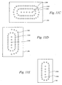
- Figure 11A illustrates a proximity head performing a wafer processing operation in accordance with one embodiment of the present invention.
- Figure 11B shows a top view of a portion of a proximity head in accordance with one embodiment of the present invention.
- Figure 11C illustrates an inlets/outlets pattern of a proximity head in accordance with one embodiment of the present invention.
- Figure 11D illustrates another inlets/outlets pattern of a proximity head in accordance with one embodiment of the present invention.
- Figure 11E illustrates a further inlets/outlets pattern of a proximity head in accordance with one embodiment of the present invention.
- the figures below illustrate embodiments of an exemplary wafer processing system proximity heads to generate a specific shape, size, and location of a fluid meniscus.
- the technology utilized herein may be known as a meniscus vacuum IPA vapor (MVIV) technology.
- This technology may be utilized to perform any suitable type of wafer operation such as, for example, meniscus vacuum IPA vapor drying (MVIVD), meniscus vacuum IPA vapor cleaning (MVIVC), meniscus vacuum IPA vapor etching (MVIVE), meniscus vacuum IPA vapor plating (MVIVP), etc.
- MVIVD meniscus vacuum IPA vapor drying
- MVIVC meniscus vacuum IPA vapor cleaning
- MVIVE meniscus vacuum IPA vapor etching
- MVIVP meniscus vacuum IPA vapor plating
- the proximity head(s) may move in a linear fashion from a center portion of the wafer to the edge of the wafer. It should be appreciated that other embodiments may be utilized where the proximity head(s) move in a linear fashion from one edge of the wafer to another diametrically opposite edge of the wafer, or other non-linear movements may be utilized such as, for example, in a radial motion, in a circular motion, in a spiral motion, in a zigzag motion, in a random motion, etc. In addition, the motion may also be any suitable specified motion profile as desired by a user. In addition, in one embodiment, the wafer may be rotated and the proximity head moved in a linear fashion so the proximity head may process all portions of the wafer.
- the proximity head and the wafer processing system as described herein may be utilized to process any shape and size of substrates such as for example, 200 mm wafers, 300 mm wafers, flat panels, etc.
- the processing system may be configured to be utilized for any suitable processing (e.g., plating, etching, cleaning, drying, etc.) of the wafer depending on the configuration of the system.
- a fluid meniscus can be supported and moved (e.g., onto, off of and across a wafer) with a proximity head.
- a coupon magazine may hold and position a docking station so the docking station can be located off the edge of the wafer and therefore simulate a wafer surface as a fluid meniscus is moved off (or on) the wafer.
- the docking station (may also be known as a coupon) can therefore provide a substantially continuous surface for the meniscus to track therefore enhancing meniscus stability.
- the coupon magazine may also be configured to level the docking station so that the docking station is substantially level (or coplanar) with the wafer being processed. By having the docking station substantially coplanar with the wafer, the fluid meniscus may move on (or off) the wafer and keep meniscus stability intact.
- FIG. 2A shows a wafer processing system 100 in accordance with one embodiment of the present invention.
- the system 100 includes rollers 102a and 102b which may hold and/or rotate a wafer to enable wafer surfaces to be processed.
- the system 100 also includes proximity heads 106a and 106b that, in one embodiment, are attached to an upper arm 104a and to a lower arm 104b respectively.
- the proximity head may be any suitable apparatus that may generate a fluid meniscus.
- the upper arm 104a and the lower arm 104b can be part of an assembly which enables substantially linear movement of the proximity heads 106a and 106b along a radius of the wafer. In yet another embodiment, the assembly may move the proximity heads 106a and 106b in any suitable user defined movement.
- the arms 104 are configured to hold the proximity head 106a above the wafer and the proximity head 106b below the wafer in close proximity to the wafer. For example, in one exemplary embodiment this may be accomplished by having the upper arm 104a and the lower arm 104b be movable in a vertical manner so once the proximity heads are moved horizontally into a location to start wafer processing, the proximity heads 106a and 106b can be moved vertically to a position in close proximity to the wafer.
- the upper arm 104a and the lower arm 104b may be configured to start the proximity heads 106a and 106b in a position where a meniscus is generated before processing and the meniscus that has already been generated between the proximity heads 106a and 106 may be moved onto the wafer surface to be processed from an edge area of a wafer 108. Therefore, the upper arm 104a and the lower arm 104b may be configured in any suitable way so the proximity heads 106a and 106b can be moved to enable wafer processing as described herein. It should also be appreciated that the system 100 may be configured in any suitable manner as long as the proximity head(s) may be moved in close proximity to the wafer to generate and control a meniscus.
- close proximity may be any suitable distance from the wafer as long as a meniscus may be maintained.
- the proximity heads 106a and 106b (as well as any other proximity head described herein) may each be located between about 0.1 mm to about 10 mm from the wafer to generate the fluid meniscus on the wafer surface.
- the proximity heads 106a and 106b may each be located bout 0.5 mm to about 2.0 mm from the wafer to generate the fluid meniscus on the wafer surface, and in more preferable embodiment, the proximity heads 106a and 106b (as well as any other proximity head described herein) may be located about 1.50 mm from the wafer to generate the fluid meniscus on the wafer surface.
- the system 100, the arms 104 are configured to enable the proximity heads 106a and 106b to be moved from processed to unprocessed portions of the wafer. It should be appreciated that the arms 104 may be movable in any suitable manner that would enable movement of the proximity heads 106a and 106b to process the wafer as desired. In one embodiment, the arms 104 may be motivated by a motor to move the proximity head 106a and 106b along the surface of the wafer. It should be understood that although the wafer processing system 100 is shown with the proximity heads 106a and 106b, that any suitable number of proximity heads may be utilized such as, for example, 1, 2, 3, 4, 5, 6, etc.
- the proximity heads 106a and/or 106b of the wafer processing system 100 may also be any suitable size or shape as shown by, for example, any of the proximity heads as described herein.
- the different configurations described herein generate a fluid meniscus between the proximity head and the wafer.
- the fluid meniscus may be moved across the wafer to process the wafer by applying fluid to the wafer surface and removing fluids from the surface. In such a way, depending on the fluids applied to the wafer, cleaning, drying, etching, and/or plating may be accomplished. Therefore, the proximity heads 106a and 106b can have any numerous types of configurations as shown herein or other configurations that enable the processes described herein. It should also be appreciated that the system 100 may process one surface of the wafer or both the top surface and the bottom surface of the wafer.
- the system 100 may also be configured to process one side of the wafer with one type of process (e.g., etching, cleaning, drying, plating, etc.) and process the other side of the wafer using the same process or a different type of process by inputting and outputting different types of fluids or by using a different configuration meniscus.
- the proximity heads can also be configured to process the bevel edge of the wafer in addition to processing the top and/or bottom of the wafer. This can be accomplished by moving the meniscus off (or onto) the edge the wafer which processes the bevel edge. It should also be understood that the proximity heads 106a and 106b may be the same type of apparatus or different types of proximity heads.
- the wafer 108 may be held and rotated by the rollers 102a and 102b in any suitable orientation as long as the orientation enables a desired proximity head to be in close proximity to a portion of the wafer 108 that is to be processed.
- the rollers 102a and 102b can rotate in a clockwise direction to rotate the wafer 108 in a counterclockwise direction. It should be understood that the rollers may be rotated in either a clockwise or a counterclockwise direction depending on the wafer rotation desired.
- the rotation imparted on the wafer 108 by the rollers 102a and 102b serves to move a wafer area that has not been processed into close proximity to the proximity heads 106a and 106b.
- the rotation itself does not dry the wafer or move fluid on the wafer surfaces towards the edge of the wafer. Therefore, in an exemplary wafer processing operation, the unprocessed areas of the wafer would be presented to the proximity heads 106a and 106b through both the linear motion of the proximity heads 106a and 106b and through the rotation of the wafer 108.
- the wafer processing operation itself may be conducted by at least one of the proximity heads. Consequently, in one embodiment, processed portions of the wafer 108 would expand from a center region to the edge region of the wafer 108 in a spiral movement as the processing operation progresses.
- the processed portions of the wafer 108 would expand from the edge region of the wafer 108 to the center region of the wafer 108 in a spiral movement.
- the proximity heads 106a and 106b may be configured to dry, clean, etch, and/or plate the wafer 108.
- the at least one of first inlet may be configured to input deionized water (DIW) (also known as a DIW inlet)
- the at least one of a second inlet may be configured to input N 2 carrier gas containing isopropyl alcohol (IPA) in vapor form (also known as IPA inlet)
- the at least one outlet may be configured to remove fluids from a region between the wafer and a particular proximity head by applying vacuum (also known as vacuum outlet).
- DIW deionized water
- IPA isopropyl alcohol
- any suitable alcohol vapor may contain any suitable types of alcohols. It should be appreciated that the any suitable alcohol can be any suitable carbon-based chemical with a hydroxy group attached to a saturated carbon atom.
- a cleaning solution may be substituted for the DIW.
- An exemplary etching embodiment may be conducted where an etchant may be substituted for the DIW.
- plating may be accomplished by using a fluid meniscus with processing fluid and proximity head configured for plating.
- other types of solutions may be inputted into the first inlet and the second inlet depending on the processing operation desired.
- the inlets and outlets located on a face of the proximity head may be in any suitable configuration as long as a stable meniscus as described herein may be utilized.
- the at least one N 2 /IPA vapor inlet may be adjacent to the at least one vacuum outlet which is in turn adjacent to the at least one processing fluid inlet to form an IPA-vacuum-processing fluid orientation.
- orientations such as IPA-processing fluid-vacuum, processing fluid-vacuum-IPA, vacuum-IPA-processing fluid, etc. may be utilized depending on the wafer processes desired and what type of wafer processing mechanism is sought to be enhanced.
- the IPA-vacuum-processing fluid orientation may be utilized to intelligently and powerfully generate, control, and move the meniscus located between a proximity head and a wafer to process wafers.
- the processing fluid inlets, the N 2 /IPA vapor inlets, and the vacuum outlets may be arranged in any suitable manner if the above orientation is maintained.
- the distance between the IPA input, vacuum, and processing fluid input locations may be varied so the distances are consistent or so the distances are inconsistent.
- the distances between the IPA input, vacuum, and processing fluid output may differ in magnitude depending on the size, shape, and configuration of the proximity head 106a and the desired size of a process meniscus (i.e., meniscus shape and size).
- exemplary IPA-vacuum-processing fluid orientation may be found as referenced herein.
- the proximity heads 106a and 106b may be positioned in close proximity to a top surface and a bottom surface respectively of the wafer 108 and may utilize the IPA and DIW inlets and a vacuum outlet(s) to generate wafer processing meniscuses in contact with the wafer 108 which are capable of processing the top surface and the bottom surface of the wafer 108.
- the wafer processing meniscus may be generated in accordance with the descriptions in reference to Applications referenced above.
- a vacuum may be applied in close proximity to the wafer surface to remove the IPA vapor, the processing fluid, and/or the fluids that may be on the wafer surface.
- IPA IPA
- any other suitable type of vapor such as for example, nitrogen, any suitable alcohol vapor, organic compounds, hexanol, ethyl glycol, acetone, etc. that may be miscible with water. These fluids may also be known as surface tension reducing fluids.
- the portion of the processing fluid that is in the region between the proximity head and the wafer is the meniscus.
- the term "output" can refer to the removal of fluid from a region between the wafer 108 and a particular proximity head, and the term “input” can be the introduction of fluid to the region between the wafer 108 and the particular proximity head.
- the fluid meniscus may be moved on (or off) of the wafer at an edge of the wafer 108.
- the system 100 includes a couple magazine 126 attached on a top surface of a wafer processing assembly.
- coupon assembly 126 includes a couple magazine 124 and top portion 122.
- the coupon assembly 126 may be configured to hold a docking station 120 in an accurate static position that is substantially planar to a wafer plane and between the proximity heads 106a and 106b.
- the docking station 120 when the docking station 120 is not substantially coplanar with the wafer plane, the docking station 120 may be adjusted with a leveling mechanism (as discussed in further detail in reference to Figure 7 ) so the wafer 108 is substantially coplanar with the docking station. Therefore, the docking station may emulate a wafer surface when the process being conducted by the proximity head 106 is ending and transitioning off of the wafer surface as described in further detail in reference to Figure 2B . It should be appreciated that the docking station 120 as described herein may be made from any suitable hydrophilic material such as, for example, quartz, ceramic, etc.
- the docking station may have a docking surface for the fluid meniscus that is adjacent to an edge of the substrate where the docking surface is in the same plane as the substrate.
- the docking surface of the docking station may provide a transition interface to allow the fluid meniscus to enter and exit the surface of the substrate.
- the docking surface has a radial contour that matches a redial contour of the substrate.
- the docking surface may provide a transition interface for a fluid meniscus of the proximity head Therefore, by providing a substantially continuous simulate wafer surface, the meniscus that is transitioning onto or off of the wafer 108 may remain stable.
- the magazine coupon 126 may be designed with a specific intent to securely hold and level a substrate of regular or irregular geometric shape in a static position for processing when using the proximity head technology.
- the magazine coupon 126 may be utilized with any suitable proximity head operation such as, for example, etching, cleaning, drying, plating, etc.
- the coupon magazine 126 is attached to a coupon magazine mount 128.
- the coupon magazine 126 and the coupon magazine mount 128 may be known as a coupon magazine assembly.
- FIG. 2B illustrates an exemplary proximity head docking operation using the docking station 120 in accordance with one embodiment of the present invention.
- the docking station 120 may include a surface 120a that may simulate an arc curvature 108a so that a meniscus formed on the wafer 108 may travel off onto the docking station 120 without a breakdown in the meniscus.
- the proximity head 126 may be moved from a location 126 of the wafer 108 to a location off of the wafer onto the docking station 120.
- the docking station is held onto place in the coupon magazine 122.
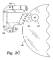
- Figure 2C shows a meniscus traveling off of the wafer 108 onto the docking station 120 in accordance with one embodiment of the present invention.
- a meniscus 140 formed by the proximity head 106 may be used to process a wafer surface of the wafer 108 as described in further detail in the Applications.
- the meniscus 140 may be moved from the wafer to a location 160.
- the location 160 includes a portion of the docking station 120 that simulates a surface of the wafer 108.
- the docking station 120 may be configured in any suitable fashion that enables the simulation of the wafer surface to keep the meniscus 140 stable.
- the docking station may be any suitable distance away from the wafer 108 that can effectively enable the docking station 120 to simulate a wafer surface as the meniscus 140 is moving off of the wafer 108.
- distance of the closest portion of the docking station 120 to the wafer is between 0.01mm and 10.0mm.
- the docking station 120 is located about 0.1mm away from the wafer 108.
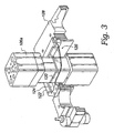
- FIG. 3 illustrates a close up view of the system 100 without some of the components to show a better view of the coupon magazine 126 in accordance with one embodiment of the present invention.
- the coupon magazine 126 may include a top portion 122 attached to a bottom portion 126.
- the top portion 122 and the bottom portion 126 may be attached with at least a portion of the docking station being located between the top portion 122 and the bottom portion 126.
- the coupon magazine 126 is a device holder that may be fabricated from chemically compatible and mechanically stable materials such as, for example, polyethylene terephthalate (PET), Polyvinylidene Fluoride (PVDF), polyetheretherketone (PEEK), etc.
- PET polyethylene terephthalate
- PVDF Polyvinylidene Fluoride
- PEEK polyetheretherketone
- the coupon magazine 126 may be machined with precise features to specific tolerances as desired.
- the coupon magazine 126 may be configured to be securely and accurately position a substrate of any suitable geometric size, shape, and thickness between, over, or under any suitable combination of proximity heads. Proximity heads as described herein and described herein may also be known as MVIV manifolds.
- the coupon magazine 126 may be used on any suitable lab test fixture or in any suitable production apparatus that may use proximity heads.
- the docking station 120 may be made substantially planar to the wafer surface by adjusting or leveling the couple magazine 126 as discussed in reference to Figure 7 . In one embodiment, either or both of the coupon magazine 126 or the coupon magazine mount 128 may be adjusted to make the docking station 120 coplanar with the wafer surface. Therefore, the coupon magazine 126 is extremely flexible in use and may intelligently and powerfully optimize wafer processing operations.
- Figure 4 depicts a more detailed view of the couple magazine 126 with a portion of the proximity head 106 showing inlets and outlets in accordance with one embodiment of the present invention.
- the coupon assembly 126 may be configured to hold the docking station 120 of any specific shape, such as, for example, a 200 mm docking state, a 300 mm docking state, etc.
- the coupon magazine 126 may also hold any suitable random shape wafer of varied size and thickness.
- Figure 5 shows the coupon magazine 126 without the proximity heads 106 in accordance with one embodiment of the present invention.
- coupon magazine 126 has a sight window 150 through which may provide access to mechanically as well as visually inspect the proximity head 106a and the proximity head 106b as shown in exemplary form in Figure 2 . In this way the distance between the proximity heads 106a and 106b as well as the distance of the proximity heads 106a and 106b may be determined.
- FIG 6 shows a top view of the coupon magazine 126 in accordance with one embodiment of the present invention.
- the coupon magazine 126 as shown may include attachment openings 320 through which the coupon magazine 126 may be bolted to the coupon magazine mount 128 as shown in Figure 2A above. It should be appreciate that any suitable number, types, and/or configurations of attachment openings 320 may be utilized to attach the coupon magazine 126 to the coupon magazine mount 128. In another embodiment, the coupon magazine 126 may be attached to the coupon magazine mount by bonding without use of attachment openings 320. The coupon magazine 126 therefore may be removed at attached to the coupon magazine mount 128 in a manner so different coupon magazines with different docking stations may be interchanged in a convenient and time saving manner.
- a portion of the outer edge of the docking state 120 is sandwiched between the top portion 122 and the bottom portion 124 of the coupon magazine 126.
- the docking station 120 may held securely during wafer processing operations.
- the docking station 120 is shown as having an opening in an interior portion, it should be appreciated that the docking station 120 may have any suitable configuration that would enable the fluid meniscus to travel from the wafer to the docking station (and vice versa) without meniscus breakdown.
- the coupon magazine 126 is shown as being rectangular in shape, the coupon magazine 126 may be any suitable shape and/or configuration as long as the docking station 120 may be held securely and the proximity heads can move on and off of the docking station 120 without interference.
- the coupon magazine may also have any suitable number of pieces such as, for example, 1, 2, 3, 4, 5, etc. as long as the docking station 120 may be held and positioned in the manner described herein.
- Figure 7 illustrates a leveling mechanism in accordance with one embodiment of the present invention.
- the leveling mechanism enables the moving of the coupon magazine in a vertical plane so the docking station 120 may be made substantially coplanar with the wafer 108.
- the top portion 122 of the coupon magazine 126 may include an access port 288 which leads to a screw 290 that ends with a ball detent 262 in the coupon magazine mount 128.
- the screw 290 may also include a spring.
- the ball detent 262 which may contact the coupon assembly mount 128.
- the spring 264 may have a force of between about 5 to 15 lbs.
- the ball detent 262 may be moved vertically and then the couple magazine 126 and in turn the docking state 120 may be moved vertically. Therefore, the coupon magazine 126 may be moved in a vertical manner so the docking station 120 is made substantially level with the wafer 108. In one embodiment, the coupon magazine 126 may be moved vertically as shown by distance 280. It should be appreciated that the apparatus and method shown to move the coupon magazine 126 is just exemplary in nature and any other suitable manner of moving the coupon magazine 126 may be utilized.
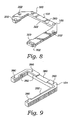
- FIG 8 shows the top portion 122 of the coupon magazine 126 in accordance with one embodiment of the present invention.
- the top portion 122 may include any suitable number and or type of attachment openings to both attach the top portion 122 to the coupon magazine mount 128 and the bottom portion 124.
- the top portion 122 may have the attachment openings 320 for bolting the top portion 122 to the coupon magazine mount 128.
- the top portion 122 may also have attachment openings 202 which may be utilized to bolt the top portion 122 to the coupon magazine mount 128.
- the top portion 122 also may include an indentation 322 which may (when combined with the bottom portion 124) generate the sight window 150 as discussed above in reference to Figure 5 .
- FIG. 9 illustrates the bottom portion 124 of the coupon magazine 126 in accordance with one embodiment of the present invention.
- the bottom portion 124 may include attachment openings 390 which may be aligned with the attachment openings 320 of the top portion 122. Therefore, by using the attachment openings 390, the bottom portion 124 may be bolted onto the top portion 122 to generate the coupon magazine 126.
- any suitable manner of attachment may be used to connect the top portion 122 to the bottom portion 124 such as, for example, gluing, bonding, etc.
- the bottom portion 124 may have any suitable number and/or configurations of attachment openings 390.
- the bottom portion 124 may also have an indentation 380 which when combined with the indentation 322 of the top portion may generate the sight window 150. In this manner, the location of the proximity heads with respect to each other and with respect to the docking station 120 may be visually and/or mechanically accessed.
- the bottom portion 124 may also have a recess 392 which substantially surrounds the perimeter of an internal portion of the bottom portion 124. The recess 392 may be configured so that the periphery of the docking station 120 fits within the recess 392 to provide a secure and snug attachment.
- the following describes an exemplary proximity head that can generate a fluid meniscus.
- FIG 10 shows a wafer processing system 1100 in accordance with one embodiment of the present invention.
- the system 1100 may include rollers 1102a, 1102b, and 1102c which can hold and rotate a wafer to enable wafer surfaces to be processed.
- the system 1100 may also include proximity heads 106a and 106b that, in one embodiment, can be attached to an upper arm 1104a and to a lower arm 1104b respectively.
- the upper arm 1104a and the lower arm 1104b can be a part of a proximity head carrier assembly 1104 which enables substantially linear movement of the proximity heads 106a and 106b along a radius of the wafer.
- the proximity head carrier assembly 1104 may be configured to hold the proximity head 106a above the wafer and the proximity head 106b below the wafer in close proximity to the wafer. This may be accomplished by having the upper arm 1104a and the lower arm 1104b be movable in a vertical manner so once the proximity heads are moved horizontally into a location to start wafer processing, the proximity heads 106a and 106b can be moved vertically to a position in close proximity to the wafer.
- the fluid meniscus may be formed between the two proximity heads 104a and 104b and moved onto the top and bottom surface of the wafer.
- the upper arm 1104a and the lower arm 1104b may be configured in any suitable way so the proximity heads 106a and 106b can be moved to enable wafer processing as described herein. It should also be appreciated that the system 1100 may be configured in any suitable manner as long as the proximity head(s) may be moved in close proximity to the wafer to generate and control a meniscus on the wafer surface.
- the proximity head 106 may be located at a first end of an arm which rotates around an axis defined by a second end of the arm. Therefore, in such an embodiment, the proximity head may be moved in an arc over the surface of the wafer.
- the arm may be moved in a combination of a rotational movement and a linear movement. Although shown with a proximity head 106 for each side of the wafer, a single head can be used for a single side of a wafer. Other surface preparation processes can be performed on sides where no proximity head 106 is used, such as a wafer scrub brush.
- the system 1100 may include a proximity head docking station that has a transition surface adjacent to the wafer.
- the fluid meniscus may transition between a docking station and the surface of the wafer while in a controlled and managed state. Again, if only one side of the wafer is desired to be processed, one arm with one proximity head may be utilized.
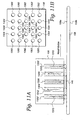
- FIG 11A illustrates a proximity head 106 performing a wafer processing operation in accordance with one embodiment of the present invention.
- the proximity head 106 moves while in close proximity to the top surface 108a of the wafer 108 to conduct the wafer processing operation.
- the fluid meniscus 140 generated by the proximity head 106 on the wafer surface 108a may be any suitable wafer processing operation such as, for example, cleaning, rinsing, drying, etching, plating, etc.
- the proximity head 106 may also be utilized to process the bottom surface 108b of the wafer 108.
- the wafer 108 may be rotated so the proximity head 106 may be moved while fluid meniscus processes the top surface 108a.
- the wafer 108 may be held still while the proximity head 106 generates the fluid meniscus on the wafer surface. Then the proximity head may move or scan over the wafer surface and therefore move the fluid meniscus along the surface of the wafer.
- the proximity head 106 may be made large enough so the fluid meniscus encompasses the surface area of the entire wafer. In such an embodiment, by applying the fluid meniscus to the surface of the wafer the entire surface of the wafer may be processed without movement of the proximity head.
- the proximity head 106 includes source inlets 1302 and 1306 and a source outlet 1304.
- isopropyl alcohol vapor in nitrogen gas IPA/N 2 1310 may be applied to the wafer surface through a source inlet 1302
- vacuum 1312 may be applied to the wafer surface through a source outlet 1304
- a processing fluid 1314 may be applied to the wafer surface through a source inlet 1306.
- the application of the IPA/N 2 1310 and the processing fluid 1314 in addition to the application of the vacuum 1312 to remove the processing fluid 1314 and the IPA/N 2 1310 from the wafer surface 108a can generate the fluid meniscus 140.
- the fluid meniscus 140 may be a fluid layer defined between the proximity head 106 and the wafer surface that can be moved across a wafer surface 108a in a stable and controllable manner.
- the fluid meniscus 140 may be defined by a constant application and removal of the processing fluid 1314.
- the fluid layer defining the fluid meniscus 140 may be any suitable shape and/or size depending on the size, number, shape, and/or pattern of the source inlets 1306, source outlets 1304 and source inlets 1302.
- any suitable flow rates of the vacuum, IPA/N 2 , vacuum, and the processing fluid may be used depending on the type of fluid meniscus desired to be generated.
- the IPA/N 2 may be omitted when generating and utilizing the fluid meniscus 106.
- the proximity head 106 may not include the source inlet 1312 and therefore only the application of the processing fluid 1314 by the source inlet 1306 and the removal of the processing fluid 1314 by the source outlet 1304 generates the fluid meniscus 140.
- the processing surface of the proximity head 106 may have any suitable topography depending on the configuration of the fluid meniscus to be generated.
- the processing surface of the proximity head may be either indented or may protrude from the surrounding surface.
- Figure 11B shows a top view of a portion of a proximity head 106 in accordance with one embodiment of the present invention.
- the configuration of the proximity head 106 as described in reference to Figure 8B is exemplary in nature. Therefore, other configurations of proximity heads may be utilized to generate the fluid meniscus as long as the processing fluid can be applied to a wafer surface and removed from the wafer surface to generate a stable fluid meniscus on the wafer surface.
- other embodiments of the proximity head 106 do not have to have the source inlet 1316 when the proximity head 106 is configured to generate the fluid meniscus without usage of N 2 /IPA.
- the source inlet 1302 from left to right are a set of the source inlet 1302, a set of the source outlet 1304, a set of the source inlet 1306, a set of the source outlet 1304, and a set of the source inlet 1302. Therefore, as N 2 /IPA and processing chemistry are inputted into the region between the proximity head 106 and the wafer 108. the vacuum removes the N 2 /IPA and the processing chemistry along with any fluid film and/or contaminants that may reside on the wafer 108.
- the source inlets 1302, the source inlets 1306, and the source outlets 1304 described herein may also be any suitable type of geometry such as for example, circular opening, triangle opening, square opening, etc.
- the source inlets 1302 and 1306 and the source outlets 1304 have circular openings.
- the proximity head 106 may be any suitable size, shape, and/or configuration depending on the size and shape of the fluid meniscus 106 desired to generated. In one embodiment, the proximity head may extend less than a radius of the wafer. In another embodiment, the proximity head may be extend more than the radius of the wafer. In another embodiment, the proximity head may extend greater than a diameter of the wafer. Therefore, the size of the fluid meniscus may be any suitable size depending on the size of a wafer surface area desired to be processed at any given time.
- the proximity head 106 may be positioned in any suitable orientation depending on the wafer processing operation such as, for example, horizontally, vertically, or any other suitable position in between.
- the proximity head 106 may also be incorporated into a wafer processing system where one or more types of wafer processing operations may be conducted.
- Figure 11C illustrates an inlets/outlets pattern of a proximity head 106 in accordance with one embodiment of the present invention.
- the proximity head 106 includes the source inlets 1302 and 1306 as well as source outlets 1304.
- the source outlets 1304 may surround the source inlets 1306 and the source inlets 1302 may surround the source outlets 1304.
- Figure 11D illustrates another inlets/outlets pattern of a proximity head 106 in accordance with one embodiment of the present invention.
- the proximity head 106 includes the source inlets 1302 and 1306 as well as source outlets 1304.
- the source outlets 1304 may surround the source inlets 1306 and the source inlets 1302 may at least partially surround the source outlets 1304.
- Figure 11E illustrates a further inlets/outlets pattern of a proximity head 106 in accordance with one embodiment of the present invention.
- the proximity head 106 includes the source inlets 1302 and 1306 as well as source outlets 1304.
- the source outlets 1304 may surround the source inlets 1306.
- the proximity head 106 does not include source inlets 1302 because, in one embodiment, the proximity head 106 is capable of generating a fluid meniscus without application of IPA/N 2 .
- the above described inlets/outlets patterns are exemplary in nature and that any suitable type of inlets/outlets patterns may be used as long as a stable and controllable fluid meniscus can be generated.
Landscapes
- Cleaning Or Drying Semiconductors (AREA)
- Exposure Of Semiconductors, Excluding Electron Or Ion Beam Exposure (AREA)
- Measurement And Recording Of Electrical Phenomena And Electrical Characteristics Of The Living Body (AREA)
- Crystals, And After-Treatments Of Crystals (AREA)
- Mechanical Treatment Of Semiconductor (AREA)
- Container, Conveyance, Adherence, Positioning, Of Wafer (AREA)
- Weting (AREA)
Claims (15)
- Vorrichtung zur Verwendung bei der Verarbeitung eines Substrats (100), umfassend:ein Couponmagazin (126) zum Halten einer Andockstation (120) für einen Annäherungskopf (106), wobei das Couponmagazin so konfiguriert ist, dass die Andockstation neben und im Wesentlichen koplanar mit einer Kante des Substrats an Ort und Stelle gehalten wird;wobei die Andockstation (120) durch eine Andockoberfläche begrenzt ist, die eine Übergangsschnittstelle (160) für einen Fluidmeniskus (140) des Annäherungskopfes vorsieht.
- Vorrichtung zur Verwendung bei der Verarbeitung eines Substrats nach Anspruch 1, wobei das Couponmagazin einen oberen Abschnitt (122) und einen unteren Abschnitt (124) einschließt.
- Vorrichtung zur Verwendung bei der Verarbeitung eines Substrats nach Anspruch 2, wobei die Andockstation zwischen dem oberen Abschnitt und dem unteren Abschnitt gehalten ist.
- Vorrichtung zur Verwendung bei der Verarbeitung eines Substrats nach Anspruch 1, wobei die Andockstation ein Quarzmaterial ist.
- Vorrichtung zur Verwendung bei der Verarbeitung eines Substrats nach Anspruch 1, wobei die Andockstation ein hydrophiles Material ist.
- Vorrichtung zur Verwendung bei der Verarbeitung eines Substrats nach Anspruch 1, weiter umfassend:eine Couponmagazinanbringung (128), die dazu konfiguriert ist, das Couponmagazin (126) zu halten.
- Vorrichtung zur Verwendung bei der Verarbeitung eines Substrats nach Anspruch 1, weiterhin mit:einem Nivellierungsmechanismus (288, 290), der dazu rekonfiguriert ist, die Andockstation so zu bewegen, dass sie im Wesentlichen koplanar mit dem Substrat ist.
- Vorrichtung zur Verwendung bei der Verarbeitung eines Substrats nach Anspruch 7, wobei der Nivellierungsmechanismus dazu konfiguriert ist, die Andockstation in einer vertikalen Ebene zu bewegen.
- Vorrichtung zur Verwendung bei der Verarbeitung eines Substrats nach Anspruch 7, wobei der Nivellierungsmechanismus (288, 290) eine Schraube (290) beinhaltet, die dazu konfiguriert ist, eine Kugelarretierung (262) vertikal zu bewegen.
- Vorrichtung zur Verwendung bei der Verarbeitung eines Substrats nach Anspruch 1, wobei das Couponmagazin ein Sichtfenster (150) beinhaltet.
- Verfahren zum Verarbeiten eines Substrats, umfassend:Positionieren einer Übergangsfläche (168), die im Wesentlichen koplanar mit einer Substratfläche ist, wobei sich die Übergangsfläche neben einer Kante des Substrats befindet; undBewegen eines Fluidmeniskus (140) zwischen der Übergangsfläche und der Substratfläche.
- Verfahren zum Verarbeiten eines Substrats nach Anspruch 11, wobei das Positionieren der Übergangsfläche das Nivellieren der Übergangsfläche einschließt.
- Verfahren zum Verarbeiten eines Substrats nach Anspruch 12, wobei das Nivellieren durch den Nivellierungsmechanismus erreicht wird.
- Verfahren zum Verarbeiten eines Substrats nach Anspruch 11, wobei die Übergangsfläche ein hydrophiles Material ist.
- Verfahren zum Verarbeiten eines Substrats nach Anspruch 11, wobei das Bewegen des Fluidmeniskus zwischen der Übergangsfläche und der Substratfläche das Bewegen des Fluidmeniskus von der Substratfläche auf die Übergangsfläche oder das Bewegen des Fluidmeniskus von der Übergangsfläche auf die Substratfläche beinhaltet.
Applications Claiming Priority (2)
| Application Number | Priority Date | Filing Date | Title |
|---|---|---|---|
| US817620 | 2004-04-01 | ||
| US10/817,620 US7513262B2 (en) | 2002-09-30 | 2004-04-01 | Substrate meniscus interface and methods for operation |
Publications (3)
| Publication Number | Publication Date |
|---|---|
| EP1583137A2 EP1583137A2 (de) | 2005-10-05 |
| EP1583137A3 EP1583137A3 (de) | 2006-04-19 |
| EP1583137B1 true EP1583137B1 (de) | 2011-06-29 |
Family
ID=34887787
Family Applications (1)
| Application Number | Title | Priority Date | Filing Date |
|---|---|---|---|
| EP05251903A Expired - Lifetime EP1583137B1 (de) | 2004-04-01 | 2005-03-29 | Substrat-Meniskus-Schnittstelle und Verfahren zum Betreiben |
Country Status (8)
| Country | Link |
|---|---|
| US (1) | US7513262B2 (de) |
| EP (1) | EP1583137B1 (de) |
| JP (1) | JP4621055B2 (de) |
| KR (1) | KR101168183B1 (de) |
| CN (1) | CN1722373B (de) |
| AT (1) | ATE515058T1 (de) |
| MY (1) | MY141428A (de) |
| SG (2) | SG115839A1 (de) |
Families Citing this family (33)
| Publication number | Priority date | Publication date | Assignee | Title |
|---|---|---|---|---|
| US7234477B2 (en) * | 2000-06-30 | 2007-06-26 | Lam Research Corporation | Method and apparatus for drying semiconductor wafer surfaces using a plurality of inlets and outlets held in close proximity to the wafer surfaces |
| US20040031167A1 (en) | 2002-06-13 | 2004-02-19 | Stein Nathan D. | Single wafer method and apparatus for drying semiconductor substrates using an inert gas air-knife |
| US7367345B1 (en) | 2002-09-30 | 2008-05-06 | Lam Research Corporation | Apparatus and method for providing a confined liquid for immersion lithography |
| US7383843B2 (en) * | 2002-09-30 | 2008-06-10 | Lam Research Corporation | Method and apparatus for processing wafer surfaces using thin, high velocity fluid layer |
| US7513262B2 (en) | 2002-09-30 | 2009-04-07 | Lam Research Corporation | Substrate meniscus interface and methods for operation |
| US7198055B2 (en) * | 2002-09-30 | 2007-04-03 | Lam Research Corporation | Meniscus, vacuum, IPA vapor, drying manifold |
| US7997288B2 (en) * | 2002-09-30 | 2011-08-16 | Lam Research Corporation | Single phase proximity head having a controlled meniscus for treating a substrate |
| US7153400B2 (en) * | 2002-09-30 | 2006-12-26 | Lam Research Corporation | Apparatus and method for depositing and planarizing thin films of semiconductor wafers |
| US7293571B2 (en) | 2002-09-30 | 2007-11-13 | Lam Research Corporation | Substrate proximity processing housing and insert for generating a fluid meniscus |
| US8236382B2 (en) * | 2002-09-30 | 2012-08-07 | Lam Research Corporation | Proximity substrate preparation sequence, and method, apparatus, and system for implementing the same |
| US7632376B1 (en) | 2002-09-30 | 2009-12-15 | Lam Research Corporation | Method and apparatus for atomic layer deposition (ALD) in a proximity system |
| US7389783B2 (en) * | 2002-09-30 | 2008-06-24 | Lam Research Corporation | Proximity meniscus manifold |
| US7614411B2 (en) | 2002-09-30 | 2009-11-10 | Lam Research Corporation | Controls of ambient environment during wafer drying using proximity head |
| US7675000B2 (en) * | 2003-06-24 | 2010-03-09 | Lam Research Corporation | System method and apparatus for dry-in, dry-out, low defect laser dicing using proximity technology |
| US8062471B2 (en) * | 2004-03-31 | 2011-11-22 | Lam Research Corporation | Proximity head heating method and apparatus |
| US7784478B2 (en) * | 2006-01-20 | 2010-08-31 | Akrion Systems Llc | Acoustic energy system, method and apparatus for processing flat articles |
| US7928366B2 (en) * | 2006-10-06 | 2011-04-19 | Lam Research Corporation | Methods of and apparatus for accessing a process chamber using a dual zone gas injector with improved optical access |
| US8813764B2 (en) | 2009-05-29 | 2014-08-26 | Lam Research Corporation | Method and apparatus for physical confinement of a liquid meniscus over a semiconductor wafer |
| US7946303B2 (en) | 2006-09-29 | 2011-05-24 | Lam Research Corporation | Carrier for reducing entrance and/or exit marks left by a substrate-processing meniscus |
| JP4755573B2 (ja) * | 2006-11-30 | 2011-08-24 | 東京応化工業株式会社 | 処理装置および処理方法、ならびに表面処理治具 |
| US8146902B2 (en) * | 2006-12-21 | 2012-04-03 | Lam Research Corporation | Hybrid composite wafer carrier for wet clean equipment |
| US8464736B1 (en) | 2007-03-30 | 2013-06-18 | Lam Research Corporation | Reclaim chemistry |
| US7975708B2 (en) * | 2007-03-30 | 2011-07-12 | Lam Research Corporation | Proximity head with angled vacuum conduit system, apparatus and method |
| US8141566B2 (en) * | 2007-06-19 | 2012-03-27 | Lam Research Corporation | System, method and apparatus for maintaining separation of liquids in a controlled meniscus |
| JP4971078B2 (ja) * | 2007-08-30 | 2012-07-11 | 東京応化工業株式会社 | 表面処理装置 |
| US9111729B2 (en) * | 2009-12-03 | 2015-08-18 | Lam Research Corporation | Small plasma chamber systems and methods |
| US9190289B2 (en) | 2010-02-26 | 2015-11-17 | Lam Research Corporation | System, method and apparatus for plasma etch having independent control of ion generation and dissociation of process gas |
| US9967965B2 (en) | 2010-08-06 | 2018-05-08 | Lam Research Corporation | Distributed, concentric multi-zone plasma source systems, methods and apparatus |
| US9155181B2 (en) | 2010-08-06 | 2015-10-06 | Lam Research Corporation | Distributed multi-zone plasma source systems, methods and apparatus |
| US8999104B2 (en) | 2010-08-06 | 2015-04-07 | Lam Research Corporation | Systems, methods and apparatus for separate plasma source control |
| US9449793B2 (en) | 2010-08-06 | 2016-09-20 | Lam Research Corporation | Systems, methods and apparatus for choked flow element extraction |
| US9177762B2 (en) | 2011-11-16 | 2015-11-03 | Lam Research Corporation | System, method and apparatus of a wedge-shaped parallel plate plasma reactor for substrate processing |
| US10283325B2 (en) | 2012-10-10 | 2019-05-07 | Lam Research Corporation | Distributed multi-zone plasma source systems, methods and apparatus |
Family Cites Families (101)
| Publication number | Priority date | Publication date | Assignee | Title |
|---|---|---|---|---|
| US3953265A (en) | 1975-04-28 | 1976-04-27 | International Business Machines Corporation | Meniscus-contained method of handling fluids in the manufacture of semiconductor wafers |
| US4086870A (en) * | 1977-06-30 | 1978-05-02 | International Business Machines Corporation | Novel resist spinning head |
| US4367123A (en) | 1980-07-09 | 1983-01-04 | Olin Corporation | Precision spot plating process and apparatus |
| JPS5852034B2 (ja) | 1981-08-26 | 1983-11-19 | 株式会社ソニツクス | 部分メツキ方法及びその装置 |
| US4444492A (en) | 1982-05-15 | 1984-04-24 | General Signal Corporation | Apparatus for projecting a series of images onto dies of a semiconductor wafer |
| US4838289A (en) * | 1982-08-03 | 1989-06-13 | Texas Instruments Incorporated | Apparatus and method for edge cleaning |
| JPS62150828A (ja) | 1985-12-25 | 1987-07-04 | Mitsubishi Electric Corp | ウエハ乾燥装置 |
| JPH0712035B2 (ja) | 1989-04-20 | 1995-02-08 | 三菱電機株式会社 | 噴流式液処理装置 |
| JPH02309638A (ja) | 1989-05-24 | 1990-12-25 | Fujitsu Ltd | ウエハーエッチング装置 |
| JPH0628223Y2 (ja) | 1989-06-14 | 1994-08-03 | 大日本スクリーン製造株式会社 | 回転塗布装置 |
| US5271774A (en) * | 1990-03-01 | 1993-12-21 | U.S. Philips Corporation | Method for removing in a centrifuge a liquid from a surface of a substrate |
| US5102494A (en) | 1990-07-13 | 1992-04-07 | Mobil Solar Energy Corporation | Wet-tip die for EFG cyrstal growth apparatus |
| US5294257A (en) * | 1991-10-28 | 1994-03-15 | International Business Machines Corporation | Edge masking spin tool |
| US5343234A (en) | 1991-11-15 | 1994-08-30 | Kuehnle Manfred R | Digital color proofing system and method for offset and gravure printing |
| US5749469A (en) * | 1992-05-15 | 1998-05-12 | Fluoroware, Inc. | Wafer carrier |
| JP2877216B2 (ja) | 1992-10-02 | 1999-03-31 | 東京エレクトロン株式会社 | 洗浄装置 |
| US5350502A (en) * | 1992-12-29 | 1994-09-27 | E. I. Du Pont De Nemours And Company | Apparatus for fluid treatment of framed membranes |
| JP2854213B2 (ja) * | 1993-03-19 | 1999-02-03 | シャープ株式会社 | 洗浄装置 |
| US5472502A (en) | 1993-08-30 | 1995-12-05 | Semiconductor Systems, Inc. | Apparatus and method for spin coating wafers and the like |
| US5807522A (en) * | 1994-06-17 | 1998-09-15 | The Board Of Trustees Of The Leland Stanford Junior University | Methods for fabricating microarrays of biological samples |
| HU222768B1 (hu) * | 1994-06-30 | 2003-10-28 | The Procter & Gamble Company | Folyadékszállító szövedék felületi energiagradienssel, eljárás előállítására és ezt tartalmazó abszorbens cikk |
| US5705223A (en) * | 1994-07-26 | 1998-01-06 | International Business Machine Corp. | Method and apparatus for coating a semiconductor wafer |
| JP3247270B2 (ja) | 1994-08-25 | 2002-01-15 | 東京エレクトロン株式会社 | 処理装置及びドライクリーニング方法 |
| US5558111A (en) | 1995-02-02 | 1996-09-24 | International Business Machines Corporation | Apparatus and method for carrier backing film reconditioning |
| US5601655A (en) | 1995-02-14 | 1997-02-11 | Bok; Hendrik F. | Method of cleaning substrates |
| JPH08277486A (ja) | 1995-04-04 | 1996-10-22 | Dainippon Printing Co Ltd | リードフレームのめっき装置 |
| TW386235B (en) * | 1995-05-23 | 2000-04-01 | Tokyo Electron Ltd | Method for spin rinsing |
| US5660642A (en) * | 1995-05-26 | 1997-08-26 | The Regents Of The University Of California | Moving zone Marangoni drying of wet objects using naturally evaporated solvent vapor |
| US5975098A (en) * | 1995-12-21 | 1999-11-02 | Dainippon Screen Mfg. Co., Ltd. | Apparatus for and method of cleaning substrate |
| DE19622015A1 (de) * | 1996-05-31 | 1997-12-04 | Siemens Ag | Verfahren zum Ätzen von Zerstörungszonen an einem Halbleitersubstratrand sowie Ätzanlage |
| US5985031A (en) | 1996-06-21 | 1999-11-16 | Micron Technology, Inc. | Spin coating spindle and chuck assembly |
| TW357406B (en) * | 1996-10-07 | 1999-05-01 | Tokyo Electron Ltd | Method and apparatus for cleaning and drying a substrate |
| DE19646006C2 (de) * | 1996-11-07 | 2000-04-06 | Hideyuki Kobayashi | Düse zur Schnellgalvanisierung mit einer Galvanisierungslösungsabstrahl- und -ansaugfunktion |
| JPH1133506A (ja) | 1997-07-24 | 1999-02-09 | Tadahiro Omi | 流体処理装置及び洗浄処理システム |
| JPH10163138A (ja) | 1996-11-29 | 1998-06-19 | Fujitsu Ltd | 半導体装置の製造方法および研磨装置 |
| JPH10232498A (ja) | 1997-02-19 | 1998-09-02 | Nec Kyushu Ltd | 現像装置 |
| US6247479B1 (en) * | 1997-05-27 | 2001-06-19 | Tokyo Electron Limited | Washing/drying process apparatus and washing/drying process method |
| JPH1131672A (ja) | 1997-07-10 | 1999-02-02 | Hitachi Ltd | 基板処理方法および基板処理装置 |
| US6103636A (en) | 1997-08-20 | 2000-08-15 | Micron Technology, Inc. | Method and apparatus for selective removal of material from wafer alignment marks |
| EP0970511B1 (de) | 1997-09-24 | 2005-01-12 | Interuniversitair Micro-Elektronica Centrum Vzw | Verfahren zum entfernen einer flüssigkeit von einer oberfläche einer substrat |
| US6491764B2 (en) * | 1997-09-24 | 2002-12-10 | Interuniversitair Microelektronics Centrum (Imec) | Method and apparatus for removing a liquid from a surface of a rotating substrate |
| DE69832567T2 (de) | 1997-09-24 | 2007-01-18 | Interuniversitair Micro-Electronica Centrum Vzw | Verfahren und Vorrichtung zum Entfernen von einer Flüssigkeit von der Oberfläche eines rotierenden Substrats |
| US6398975B1 (en) * | 1997-09-24 | 2002-06-04 | Interuniversitair Microelektronica Centrum (Imec) | Method and apparatus for localized liquid treatment of the surface of a substrate |
| EP0905746A1 (de) | 1997-09-24 | 1999-03-31 | Interuniversitair Micro-Elektronica Centrum Vzw | Verfahren zum Entfernen einer Flüssigkeit von einer Oberfläche einer umlaufenden Substrat |
| JP3523197B2 (ja) * | 1998-02-12 | 2004-04-26 | エーシーエム リサーチ,インコーポレイティド | メッキ設備及び方法 |
| JPH11233475A (ja) * | 1998-02-12 | 1999-08-27 | Sony Corp | 基板洗浄装置 |
| WO1999049504A1 (fr) | 1998-03-26 | 1999-09-30 | Nikon Corporation | Procede et systeme d'exposition par projection |
| US6108932A (en) | 1998-05-05 | 2000-08-29 | Steag Microtech Gmbh | Method and apparatus for thermocapillary drying |
| JPH11350169A (ja) | 1998-06-10 | 1999-12-21 | Chemitoronics Co | ウエットエッチング装置およびウエットエッチングの方法 |
| US6132586A (en) * | 1998-06-11 | 2000-10-17 | Integrated Process Equipment Corporation | Method and apparatus for non-contact metal plating of semiconductor wafers using a bipolar electrode assembly |
| US6689323B2 (en) | 1998-10-30 | 2004-02-10 | Agilent Technologies | Method and apparatus for liquid transfer |
| US6715944B2 (en) * | 1998-11-12 | 2004-04-06 | Mitsubishi Denki Kabushiki Kaisha | Apparatus for removing photoresist film |
| US6092937A (en) | 1999-01-08 | 2000-07-25 | Fastar, Ltd. | Linear developer |
| JP2000271524A (ja) * | 1999-03-25 | 2000-10-03 | Tokyo Electron Ltd | 処理装置及び処理方法 |
| JP3653198B2 (ja) * | 1999-07-16 | 2005-05-25 | アルプス電気株式会社 | 乾燥用ノズルおよびこれを用いた乾燥装置ならびに洗浄装置 |
| US20020121290A1 (en) * | 1999-08-25 | 2002-09-05 | Applied Materials, Inc. | Method and apparatus for cleaning/drying hydrophobic wafers |
| JP3635217B2 (ja) * | 1999-10-05 | 2005-04-06 | 東京エレクトロン株式会社 | 液処理装置及びその方法 |
| WO2001027357A1 (en) | 1999-10-12 | 2001-04-19 | Semitool, Inc. | Method and apparatus for executing plural processes on a microelectronic workpiece at a single processing station |
| US6341998B1 (en) * | 1999-11-04 | 2002-01-29 | Vlsi Technology, Inc. | Integrated circuit (IC) plating deposition system and method |
| US6162302A (en) * | 1999-11-16 | 2000-12-19 | Agilent Technologies | Method of cleaning quartz substrates using conductive solutions |
| US6214513B1 (en) | 1999-11-24 | 2001-04-10 | Xerox Corporation | Slot coating under an electric field |
| US6433541B1 (en) | 1999-12-23 | 2002-08-13 | Kla-Tencor Corporation | In-situ metalization monitoring using eddy current measurements during the process for removing the film |
| US20030091754A1 (en) | 2000-02-11 | 2003-05-15 | Thami Chihani | Method for treating cellulosic fibres |
| US6474786B2 (en) | 2000-02-24 | 2002-11-05 | The Board Of Trustees Of The Leland Stanford Junior University | Micromachined two-dimensional array droplet ejectors |
| US6495005B1 (en) | 2000-05-01 | 2002-12-17 | International Business Machines Corporation | Electroplating apparatus |
| AU2001261625B2 (en) | 2000-05-16 | 2006-04-06 | Regents Of The University Of Minnesota | High mass throughput particle generation using multiple nozzle spraying |
| AU2001270205A1 (en) | 2000-06-26 | 2002-01-08 | Applied Materials, Inc. | Method and apparatus for wafer cleaning |
| US7234477B2 (en) | 2000-06-30 | 2007-06-26 | Lam Research Corporation | Method and apparatus for drying semiconductor wafer surfaces using a plurality of inlets and outlets held in close proximity to the wafer surfaces |
| US7000622B2 (en) | 2002-09-30 | 2006-02-21 | Lam Research Corporation | Methods and systems for processing a bevel edge of a substrate using a dynamic liquid meniscus |
| US6488040B1 (en) * | 2000-06-30 | 2002-12-03 | Lam Research Corporation | Capillary proximity heads for single wafer cleaning and drying |
| US6530823B1 (en) | 2000-08-10 | 2003-03-11 | Nanoclean Technologies Inc | Methods for cleaning surfaces substantially free of contaminants |
| JP2002075947A (ja) * | 2000-08-30 | 2002-03-15 | Alps Electric Co Ltd | ウェット処理装置 |
| US6555017B1 (en) | 2000-10-13 | 2003-04-29 | The Regents Of The University Of Caliofornia | Surface contouring by controlled application of processing fluid using Marangoni effect |
| US6550988B2 (en) | 2000-10-30 | 2003-04-22 | Dainippon Screen Mfg., Co., Ltd. | Substrate processing apparatus |
| US6531206B2 (en) * | 2001-02-07 | 2003-03-11 | 3M Innovative Properties Company | Microstructured surface film assembly for liquid acquisition and transport |
| WO2002101798A2 (en) | 2001-06-12 | 2002-12-19 | Verteq, Inc. | Method of applying liquid to a megasonic apparatus for improved cleaning control |
| TW554069B (en) | 2001-08-10 | 2003-09-21 | Ebara Corp | Plating device and method |
| JP2003115474A (ja) | 2001-10-03 | 2003-04-18 | Ebara Corp | 基板処理装置及び方法 |
| JP4003441B2 (ja) | 2001-11-08 | 2007-11-07 | セイコーエプソン株式会社 | 表面処理装置および表面処理方法 |
| US6799584B2 (en) | 2001-11-09 | 2004-10-05 | Applied Materials, Inc. | Condensation-based enhancement of particle removal by suction |
| KR100459710B1 (ko) * | 2002-04-15 | 2004-12-04 | 삼성전자주식회사 | 웨이퍼 세정 장비 |
| US7513262B2 (en) | 2002-09-30 | 2009-04-07 | Lam Research Corporation | Substrate meniscus interface and methods for operation |
| US7614411B2 (en) | 2002-09-30 | 2009-11-10 | Lam Research Corporation | Controls of ambient environment during wafer drying using proximity head |
| US7093375B2 (en) | 2002-09-30 | 2006-08-22 | Lam Research Corporation | Apparatus and method for utilizing a meniscus in substrate processing |
| PL208010B1 (pl) | 2002-09-30 | 2011-03-31 | Lam Res Corp | Sposób obróbki płytek półprzewodnikowych i głowica do przygotowania powierzchni płytek półprzewodnikowych |
| US7153400B2 (en) | 2002-09-30 | 2006-12-26 | Lam Research Corporation | Apparatus and method for depositing and planarizing thin films of semiconductor wafers |
| US7383843B2 (en) | 2002-09-30 | 2008-06-10 | Lam Research Corporation | Method and apparatus for processing wafer surfaces using thin, high velocity fluid layer |
| US6988326B2 (en) | 2002-09-30 | 2006-01-24 | Lam Research Corporation | Phobic barrier meniscus separation and containment |
| US7252097B2 (en) | 2002-09-30 | 2007-08-07 | Lam Research Corporation | System and method for integrating in-situ metrology within a wafer process |
| US6988327B2 (en) | 2002-09-30 | 2006-01-24 | Lam Research Corporation | Methods and systems for processing a substrate using a dynamic liquid meniscus |
| US7389783B2 (en) | 2002-09-30 | 2008-06-24 | Lam Research Corporation | Proximity meniscus manifold |
| US6954993B1 (en) | 2002-09-30 | 2005-10-18 | Lam Research Corporation | Concentric proximity processing head |
| US7293571B2 (en) | 2002-09-30 | 2007-11-13 | Lam Research Corporation | Substrate proximity processing housing and insert for generating a fluid meniscus |
| US7198055B2 (en) | 2002-09-30 | 2007-04-03 | Lam Research Corporation | Meniscus, vacuum, IPA vapor, drying manifold |
| US7069937B2 (en) | 2002-09-30 | 2006-07-04 | Lam Research Corporation | Vertical proximity processor |
| SG121822A1 (en) | 2002-11-12 | 2006-05-26 | Asml Netherlands Bv | Lithographic apparatus and device manufacturing method |
| US7270137B2 (en) * | 2003-04-28 | 2007-09-18 | Tokyo Electron Limited | Apparatus and method of securing a workpiece during high-pressure processing |
| EP1489461A1 (de) | 2003-06-11 | 2004-12-22 | ASML Netherlands B.V. | Lithographischer Apparat und Verfahren zur Herstellung einer Vorrichtung |
| US6867844B2 (en) | 2003-06-19 | 2005-03-15 | Asml Holding N.V. | Immersion photolithography system and method using microchannel nozzles |
| US7353560B2 (en) | 2003-12-18 | 2008-04-08 | Lam Research Corporation | Proximity brush unit apparatus and method |
| US7003899B1 (en) | 2004-09-30 | 2006-02-28 | Lam Research Corporation | System and method for modulating flow through multiple ports in a proximity head |
-
2004
- 2004-04-01 US US10/817,620 patent/US7513262B2/en not_active Expired - Fee Related
-
2005
- 2005-03-23 SG SG200502528A patent/SG115839A1/en unknown
- 2005-03-23 SG SG200708776-0A patent/SG136141A1/en unknown
- 2005-03-29 AT AT05251903T patent/ATE515058T1/de not_active IP Right Cessation
- 2005-03-29 EP EP05251903A patent/EP1583137B1/de not_active Expired - Lifetime
- 2005-03-31 JP JP2005100372A patent/JP4621055B2/ja not_active Expired - Fee Related
- 2005-04-01 MY MYPI20051479A patent/MY141428A/en unknown
- 2005-04-01 CN CN2005100741974A patent/CN1722373B/zh not_active Expired - Fee Related
- 2005-04-01 KR KR1020050027441A patent/KR101168183B1/ko not_active Expired - Fee Related
Also Published As
| Publication number | Publication date |
|---|---|
| JP4621055B2 (ja) | 2011-01-26 |
| MY141428A (en) | 2010-04-30 |
| US7513262B2 (en) | 2009-04-07 |
| SG136141A1 (en) | 2007-10-29 |
| JP2005294835A (ja) | 2005-10-20 |
| US20050145268A1 (en) | 2005-07-07 |
| CN1722373B (zh) | 2011-09-28 |
| EP1583137A3 (de) | 2006-04-19 |
| ATE515058T1 (de) | 2011-07-15 |
| CN1722373A (zh) | 2006-01-18 |
| KR20060045411A (ko) | 2006-05-17 |
| EP1583137A2 (de) | 2005-10-05 |
| KR101168183B1 (ko) | 2012-07-24 |
| SG115839A1 (en) | 2005-10-28 |
Similar Documents
| Publication | Publication Date | Title |
|---|---|---|
| EP1583137B1 (de) | Substrat-Meniskus-Schnittstelle und Verfahren zum Betreiben | |
| US7731802B2 (en) | Methods for transitioning a fluid meniscus to and from surfaces of a substrate | |
| EP1582269B1 (de) | Naher Fluidmeniskusverteiler | |
| EP1583136B1 (de) | Kontrolle der Raumumgebung während des Trocknen von Wafern | |
| US6954993B1 (en) | Concentric proximity processing head | |
| EP1583138A1 (de) | Ein Verfahren und eine Vorrichtung um Waferoberflächen zu behandeln | |
| EP1601006B1 (de) | Eine Vorrichtung und ein Verfahren um ein Fluidmeniskus herzustellen | |
| US7862663B2 (en) | Methods for processing a substrate with a flow controlled meniscus | |
| US7192488B2 (en) | Methods and systems for processing a bevel edge of a substrate using a dynamic liquid meniscus | |
| US7387689B2 (en) | Methods for drying semiconductor wafer surfaces using a plurality of inlets and outlets held in close proximity to the wafer surfaces | |
| WO2004030051A2 (en) | System for substrate processing with meniscus, vacuum, ipa vapor, drying manifold |
Legal Events
| Date | Code | Title | Description |
|---|---|---|---|
| PUAI | Public reference made under article 153(3) epc to a published international application that has entered the european phase |
Free format text: ORIGINAL CODE: 0009012 |
|
| AK | Designated contracting states |
Kind code of ref document: A2 Designated state(s): AT BE BG CH CY CZ DE DK EE ES FI FR GB GR HU IE IS IT LI LT LU MC NL PL PT RO SE SI SK TR |
|
| AX | Request for extension of the european patent |
Extension state: AL BA HR LV MK YU |
|
| PUAL | Search report despatched |
Free format text: ORIGINAL CODE: 0009013 |
|
| AK | Designated contracting states |
Kind code of ref document: A3 Designated state(s): AT BE BG CH CY CZ DE DK EE ES FI FR GB GR HU IE IS IT LI LT LU MC NL PL PT RO SE SI SK TR |
|
| AX | Request for extension of the european patent |
Extension state: AL BA HR LV MK YU |
|
| 17P | Request for examination filed |
Effective date: 20060915 |
|
| AKX | Designation fees paid |
Designated state(s): AT BE BG CH CY CZ DE DK EE ES FI FR GB GR HU IE IS IT LI LT LU MC NL PL PT RO SE SI SK TR |
|
| 17Q | First examination report despatched |
Effective date: 20090417 |
|
| GRAP | Despatch of communication of intention to grant a patent |
Free format text: ORIGINAL CODE: EPIDOSNIGR1 |
|
| GRAS | Grant fee paid |
Free format text: ORIGINAL CODE: EPIDOSNIGR3 |
|
| GRAA | (expected) grant |
Free format text: ORIGINAL CODE: 0009210 |
|
| AK | Designated contracting states |
Kind code of ref document: B1 Designated state(s): AT BE BG CH CY CZ DE DK EE ES FI FR GB GR HU IE IS IT LI LT LU MC NL PL PT RO SE SI SK TR |
|
| REG | Reference to a national code |
Ref country code: GB Ref legal event code: FG4D |
|
| REG | Reference to a national code |
Ref country code: CH Ref legal event code: EP |
|
| REG | Reference to a national code |
Ref country code: IE Ref legal event code: FG4D |
|
| REG | Reference to a national code |
Ref country code: DE Ref legal event code: R096 Ref document number: 602005028716 Country of ref document: DE Effective date: 20110908 |
|
| REG | Reference to a national code |
Ref country code: NL Ref legal event code: VDEP Effective date: 20110629 |
|
| PG25 | Lapsed in a contracting state [announced via postgrant information from national office to epo] |
Ref country code: SE Free format text: LAPSE BECAUSE OF FAILURE TO SUBMIT A TRANSLATION OF THE DESCRIPTION OR TO PAY THE FEE WITHIN THE PRESCRIBED TIME-LIMIT Effective date: 20110629 Ref country code: LT Free format text: LAPSE BECAUSE OF FAILURE TO SUBMIT A TRANSLATION OF THE DESCRIPTION OR TO PAY THE FEE WITHIN THE PRESCRIBED TIME-LIMIT Effective date: 20110629 |
|
| PG25 | Lapsed in a contracting state [announced via postgrant information from national office to epo] |
Ref country code: FI Free format text: LAPSE BECAUSE OF FAILURE TO SUBMIT A TRANSLATION OF THE DESCRIPTION OR TO PAY THE FEE WITHIN THE PRESCRIBED TIME-LIMIT Effective date: 20110629 Ref country code: SI Free format text: LAPSE BECAUSE OF FAILURE TO SUBMIT A TRANSLATION OF THE DESCRIPTION OR TO PAY THE FEE WITHIN THE PRESCRIBED TIME-LIMIT Effective date: 20110629 Ref country code: GR Free format text: LAPSE BECAUSE OF FAILURE TO SUBMIT A TRANSLATION OF THE DESCRIPTION OR TO PAY THE FEE WITHIN THE PRESCRIBED TIME-LIMIT Effective date: 20110930 Ref country code: AT Free format text: LAPSE BECAUSE OF FAILURE TO SUBMIT A TRANSLATION OF THE DESCRIPTION OR TO PAY THE FEE WITHIN THE PRESCRIBED TIME-LIMIT Effective date: 20110629 |
|
| PG25 | Lapsed in a contracting state [announced via postgrant information from national office to epo] |
Ref country code: BE Free format text: LAPSE BECAUSE OF FAILURE TO SUBMIT A TRANSLATION OF THE DESCRIPTION OR TO PAY THE FEE WITHIN THE PRESCRIBED TIME-LIMIT Effective date: 20110629 |
|
| PG25 | Lapsed in a contracting state [announced via postgrant information from national office to epo] |
Ref country code: EE Free format text: LAPSE BECAUSE OF FAILURE TO SUBMIT A TRANSLATION OF THE DESCRIPTION OR TO PAY THE FEE WITHIN THE PRESCRIBED TIME-LIMIT Effective date: 20110629 Ref country code: NL Free format text: LAPSE BECAUSE OF FAILURE TO SUBMIT A TRANSLATION OF THE DESCRIPTION OR TO PAY THE FEE WITHIN THE PRESCRIBED TIME-LIMIT Effective date: 20110629 Ref country code: PT Free format text: LAPSE BECAUSE OF FAILURE TO SUBMIT A TRANSLATION OF THE DESCRIPTION OR TO PAY THE FEE WITHIN THE PRESCRIBED TIME-LIMIT Effective date: 20111031 Ref country code: IS Free format text: LAPSE BECAUSE OF FAILURE TO SUBMIT A TRANSLATION OF THE DESCRIPTION OR TO PAY THE FEE WITHIN THE PRESCRIBED TIME-LIMIT Effective date: 20111029 Ref country code: CZ Free format text: LAPSE BECAUSE OF FAILURE TO SUBMIT A TRANSLATION OF THE DESCRIPTION OR TO PAY THE FEE WITHIN THE PRESCRIBED TIME-LIMIT Effective date: 20110629 |
|
| PG25 | Lapsed in a contracting state [announced via postgrant information from national office to epo] |
Ref country code: PL Free format text: LAPSE BECAUSE OF FAILURE TO SUBMIT A TRANSLATION OF THE DESCRIPTION OR TO PAY THE FEE WITHIN THE PRESCRIBED TIME-LIMIT Effective date: 20110629 Ref country code: RO Free format text: LAPSE BECAUSE OF FAILURE TO SUBMIT A TRANSLATION OF THE DESCRIPTION OR TO PAY THE FEE WITHIN THE PRESCRIBED TIME-LIMIT Effective date: 20110629 Ref country code: SK Free format text: LAPSE BECAUSE OF FAILURE TO SUBMIT A TRANSLATION OF THE DESCRIPTION OR TO PAY THE FEE WITHIN THE PRESCRIBED TIME-LIMIT Effective date: 20110629 Ref country code: CY Free format text: LAPSE BECAUSE OF FAILURE TO SUBMIT A TRANSLATION OF THE DESCRIPTION OR TO PAY THE FEE WITHIN THE PRESCRIBED TIME-LIMIT Effective date: 20110629 |
|
| PLBE | No opposition filed within time limit |
Free format text: ORIGINAL CODE: 0009261 |
|
| STAA | Information on the status of an ep patent application or granted ep patent |
Free format text: STATUS: NO OPPOSITION FILED WITHIN TIME LIMIT |
|
| PG25 | Lapsed in a contracting state [announced via postgrant information from national office to epo] |
Ref country code: IT Free format text: LAPSE BECAUSE OF FAILURE TO SUBMIT A TRANSLATION OF THE DESCRIPTION OR TO PAY THE FEE WITHIN THE PRESCRIBED TIME-LIMIT Effective date: 20110629 |
|
| 26N | No opposition filed |
Effective date: 20120330 |
|
| PG25 | Lapsed in a contracting state [announced via postgrant information from national office to epo] |
Ref country code: DK Free format text: LAPSE BECAUSE OF FAILURE TO SUBMIT A TRANSLATION OF THE DESCRIPTION OR TO PAY THE FEE WITHIN THE PRESCRIBED TIME-LIMIT Effective date: 20110629 |
|
| REG | Reference to a national code |
Ref country code: DE Ref legal event code: R097 Ref document number: 602005028716 Country of ref document: DE Effective date: 20120330 |
|
| PG25 | Lapsed in a contracting state [announced via postgrant information from national office to epo] |
Ref country code: MC Free format text: LAPSE BECAUSE OF NON-PAYMENT OF DUE FEES Effective date: 20120331 |
|
| REG | Reference to a national code |
Ref country code: CH Ref legal event code: PL |
|
| GBPC | Gb: european patent ceased through non-payment of renewal fee |
Effective date: 20120329 |
|
| REG | Reference to a national code |
Ref country code: FR Ref legal event code: ST Effective date: 20121130 |
|
| REG | Reference to a national code |
Ref country code: IE Ref legal event code: MM4A |
|
| PG25 | Lapsed in a contracting state [announced via postgrant information from national office to epo] |
Ref country code: CH Free format text: LAPSE BECAUSE OF NON-PAYMENT OF DUE FEES Effective date: 20120331 Ref country code: GB Free format text: LAPSE BECAUSE OF NON-PAYMENT OF DUE FEES Effective date: 20120329 Ref country code: FR Free format text: LAPSE BECAUSE OF NON-PAYMENT OF DUE FEES Effective date: 20120402 Ref country code: IE Free format text: LAPSE BECAUSE OF NON-PAYMENT OF DUE FEES Effective date: 20120329 Ref country code: LI Free format text: LAPSE BECAUSE OF NON-PAYMENT OF DUE FEES Effective date: 20120331 |
|
| PG25 | Lapsed in a contracting state [announced via postgrant information from national office to epo] |
Ref country code: ES Free format text: LAPSE BECAUSE OF FAILURE TO SUBMIT A TRANSLATION OF THE DESCRIPTION OR TO PAY THE FEE WITHIN THE PRESCRIBED TIME-LIMIT Effective date: 20111010 |
|
| PGFP | Annual fee paid to national office [announced via postgrant information from national office to epo] |
Ref country code: DE Payment date: 20130327 Year of fee payment: 9 |
|
| PG25 | Lapsed in a contracting state [announced via postgrant information from national office to epo] |
Ref country code: BG Free format text: LAPSE BECAUSE OF FAILURE TO SUBMIT A TRANSLATION OF THE DESCRIPTION OR TO PAY THE FEE WITHIN THE PRESCRIBED TIME-LIMIT Effective date: 20110929 |
|
| PG25 | Lapsed in a contracting state [announced via postgrant information from national office to epo] |
Ref country code: TR Free format text: LAPSE BECAUSE OF FAILURE TO SUBMIT A TRANSLATION OF THE DESCRIPTION OR TO PAY THE FEE WITHIN THE PRESCRIBED TIME-LIMIT Effective date: 20110629 |
|
| PG25 | Lapsed in a contracting state [announced via postgrant information from national office to epo] |
Ref country code: LU Free format text: LAPSE BECAUSE OF NON-PAYMENT OF DUE FEES Effective date: 20120329 |
|
| PG25 | Lapsed in a contracting state [announced via postgrant information from national office to epo] |
Ref country code: HU Free format text: LAPSE BECAUSE OF FAILURE TO SUBMIT A TRANSLATION OF THE DESCRIPTION OR TO PAY THE FEE WITHIN THE PRESCRIBED TIME-LIMIT Effective date: 20050329 |
|
| REG | Reference to a national code |
Ref country code: DE Ref legal event code: R119 Ref document number: 602005028716 Country of ref document: DE |
|
| REG | Reference to a national code |
Ref country code: DE Ref legal event code: R119 Ref document number: 602005028716 Country of ref document: DE Effective date: 20141001 |
|
| PG25 | Lapsed in a contracting state [announced via postgrant information from national office to epo] |
Ref country code: DE Free format text: LAPSE BECAUSE OF NON-PAYMENT OF DUE FEES Effective date: 20141001 |